Emission characteristics of optically pumped GaN-based vertical-cavity
surface-emitting lasers
Jung-Tang Chu, Tien-Chang Lu, Min You, Bor-Jye Su, Chih-Chiang Kao, Hao-Chung Kuo, and Shing-Chung Wang
Citation: Applied Physics Letters 89, 121112 (2006); doi: 10.1063/1.2355476
View online: http://dx.doi.org/10.1063/1.2355476
View Table of Contents: http://scitation.aip.org/content/aip/journal/apl/89/12?ver=pdfcov Published by the AIP Publishing
Articles you may be interested in
Blue 6-ps short-pulse generation in gain-switched InGaN vertical-cavity surface-emitting lasers via impulsive optical pumping
Appl. Phys. Lett. 101, 191108 (2012); 10.1063/1.4766290
Continuous wave operation of current injected GaN vertical cavity surface emitting lasers at room temperature Appl. Phys. Lett. 97, 071114 (2010); 10.1063/1.3483133
Fabrication and performance of blue GaN-based vertical-cavity surface emitting laser employing AlN GaN and Ta 2 O 5 SiO 2 distributed Bragg reflector
Appl. Phys. Lett. 87, 081105 (2005); 10.1063/1.2032598
Low-threshold lasing of InGaN vertical-cavity surface-emitting lasers with dielectric distributed Bragg reflectors Appl. Phys. Lett. 83, 830 (2003); 10.1063/1.1596728
Observation of enhanced spontaneous emission coupling factor in nitride-based vertical-cavity surface-emitting laser
Appl. Phys. Lett. 80, 722 (2002); 10.1063/1.1430855
This article is copyrighted as indicated in the article. Reuse of AIP content is subject to the terms at: http://scitation.aip.org/termsconditions. Downloaded to IP: 140.113.38.11 On: Thu, 01 May 2014 01:47:33
Emission characteristics of optically pumped GaN-based vertical-cavity
surface-emitting lasers
Jung-Tang Chu, Tien-Chang Lu, Min You, Bor-Jye Su, Chih-Chiang Kao, Hao-Chung Kuo, and Shing-Chung Wanga兲
Department of Photonics, National Chiao Tung University, 1001 Ta Hsueh Road, Hsinchu, Taiwan 300, Taiwan and Institute of Electro-Optical Engineering, National Chiao Tung University, 1001 Ta Hsueh Road, Hsinchu, Taiwan 300, Taiwan
共Received 5 July 2006; accepted 5 August 2006; published online 20 September 2006兲
The laser emission characteristics of a GaN-based vertical-cavity surface-emitting laser with two dielectric distributed Bragg reflectors were investigated under optically pumped operation at room temperature. The laser emitted wavelength at 415.9 nm with an emission linewidth of 0.25 nm and threshold pumping energy of 270 nJ. The laser has a high characteristic temperature of about 278 K and high spontaneous emission coupling factor of 10−2. The laser emission showed single and
multiple spot emission patterns with spectral and spatial variations under different pumping conditions. © 2006 American Institute of Physics.关DOI:10.1063/1.2355476兴
GaN-based blue/violet vertical-cavity surface-emitting lasers共VCSELs兲 have attracted much attention due to many advantageous properties over edge-emitting lasers, including circular beam shapes, light emission in the vertical direction, and two-dimensional arrays on the wafer level. A VCSEL structure is made up by a microcavity with a few wave-lengths in length and a pair of high reflectivity共above 99%兲 distributed Bragg reflectors 共DBRs兲 necessary for reducing the lasing threshold. Efforts to obtain optically pumped stimulated emission in GaN-based VCSELs have been re-ported by several groups.1–4. Somlya et al.1and Zhou et al.2 demonstrated lasing operations of VCSELs with the structure of monolithically grown AlGaN / GaN DBRs, GaN / InGaN microcavities, and dielectric DBRs.2 GaN-based VCSELs with two dielectric DBRs were also proposed by Song et al.3 and Tawara et al.4Our group has demonstrated initial lasing behaviors in two types of GaN VCSELs: one with hybrid-type DBRs which has a dielectric DBR and an epitaxially grown AlN / GaN DBR,5 the other is a dielectric-type VC-SEL comprising a GaN active region and two dielectric DBRs.6 In this study, we report the detailed laser emission properties of the dielectric-type GaN-based VCSEL optically pumped at room temperature. The below and above thresh-old behaviors of laser emission intensity and temperature dependence of the threshold pumping energy were investi-gated. High spontaneous emission factor and high character-istic temperature were obtained. The laser emission proper-ties showed the dependence of emission spectrum on pumping energy. Single and multiple spot emission patterns were observed spatially and spectrally, indicating a highly inhomogeneous gain distribution in the InGaN / GaN mul-tiple quantum well共MQW兲 layers.
The VCSEL layer structure grown on a共0001兲-oriented sapphire substrate by metal organic chemical vapor deposi-tion included a 30 nm GaN nucleadeposi-tion layer, a 4m GaN bulk layer, MQWs consisting of ten periods of 5 nm GaN barriers and 3 nm In0.1Ga0.9N wells, and a 200 nm GaN cap layer. Six pairs of SiO2and TiO2were evaporated on the top
of the grown VCSEL structure to form the first dielectric DBR. The reflectivity of the SiO2/ TiO2DBR at 416 nm was
99.5%. Next, an array of circular SiO2/ TiO2 DBR mesas
with diameters of 60m was formed by standard lithogra-phy and chemical wet etching process. To deposit the second dielectric DBR, the structure was subjected to a laser lift-off 共LLO兲 process using a KrF excimer laser to remove the sap-phire substrate. The GaN surface after LLO was further pol-ished and obtained a surface roughness of about 1 nm for deposition of the second dielectric DBR consisting of eight pairs of SiO2and Ta2O5. The final thickness of the epitaxial
structure after LLO and polishing process was about 4m. The Ta2O5was used to reduce the absorption of the pumping beam at a wavelength of 355 nm. The reflectivity of the SiO2/ Ta2O5DBR at 416 nm was 97%. For the detailed
pro-cess procedure, please refer to our previous report.6
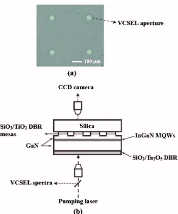
Figure 1共a兲 shows the microscopic image of a fabricated
a兲Electronic mail: [email protected] FIG. 1.array.共b兲 Schematic structure of the VCSEL and experiment setup.共Color online兲 共a兲 Microscopic top view image of a 2⫻2 VCSEL APPLIED PHYSICS LETTERS 89, 121112共2006兲
0003-6951/2006/89共12兲/121112/3/$23.00 89, 121112-1 © 2006 American Institute of Physics
This article is copyrighted as indicated in the article. Reuse of AIP content is subject to the terms at: http://scitation.aip.org/termsconditions. Downloaded to IP: 140.113.38.11 On: Thu, 01 May 2014 01:47:33
2⫻2 VCSEL array. The circular areas are the locations of VCSELs with DBRs, also serving the emission apertures. The fabricated GaN-based VCSELs were optically pumped by a Nd: YVO4 laser at 355 nm, with a repetition rate of
1 kHz and a pulse width of 0.5 ns. As shown in Fig. 1共b兲, the pumping laser beam with a focused spot size of about 40m in diameter was vertically incident on the VCSEL sample from the SiO2/ Ta2O5DBR side. The light emission from the
VCSEL sample was collected by an imaging optic into a spectrometer with a spectral resolution of 0.1 nm. The emis-sion patterns were detected by a charge coupled device cam-era from the SiO2/ TiO5 DBR side through the mesa
aper-ture. The dependence of threshold pumping energies on the temperature was measured from 58 to 322 K using a temperature-controlled cryogenic chamber.
The laser emission intensity as the function of pumping energy is shown in Fig. 2共a兲 in a semilogarithmic scale. A clear evidence of threshold behavior was observed at a pumping energy of Eth= 270 nJ corresponding to an energy
density of 21.5 mJ/ cm2. The inset shows the spectrum of the
laser emission with a wavelength of 415.9 nm and a narrow linewidth of about 0.25 nm. From the semilogarithmic data, the spontaneous emission factor, which indicated the cou-pling efficiency of the spontaneous emission to the lasing
mode, was estimated from the difference between the heights of the emission intensities before and after lasing was esti-mated as about 2⫻10−2, which was in agreement with the
reported results4,7and was nearly three orders of magnitude higher than that of the typical GaN edge-emitting semicon-ductor lasers,1 indicating the enhancement of the spontane-ous emission into a lasing mode by the high cavity quality factor 共cavity Q factor兲 of the microcavity of the VCSEL structure.
The temperature dependence of the lasing threshold of the VCSEL is shown in Fig. 2共b兲. The threshold pumping energy increased gradually with increasing temperature. The dependence of the threshold condition on the temperature can be expressed as Eth共T兲=E0exp共T/T0兲, where E0is a
con-stant and T0 is the characteristic temperature. We obtain a
characteristic temperature of about 278 K for this dielectric-type VCSEL for the temperature range of 58– 322 K by lin-early fitting the experimental result. This T0value is close to the T0value of 300 K for GaN-based VCSELs predicted by Honda et al.,8and higher than the reported T0of 170 K共Ref.
9兲 or 235 K 共Ref. 10兲 for the GaN-based edge-emitting laser diode. This T0value is also higher than the T0 value for the
hybrid DBR VCSEL we reported earlier.11The high T0value could be attributed to a better gain alignment of the MQWs with the cavity mode and a lower threshold carrier density due to the higher quality factor provided by both dielectric DBRs.
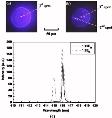
The laser emission patterns from the aperture show single spot and multiple spot emission patterns under differ-ent pumping conditions, as shown in Figs. 3共a兲 and 3共b兲 at pumping energies of 1.15Eth and 1.2Eth. The lasing
wave-length from each emission spot also differed in few nanom-eters. At low pumping energy, the emission pattern showed a single spot with a spot size of about 3m. As the pumping FIG. 2.共a兲 Laser emission intensity vs pumping energy in semilogarithmic
scale. The value estimated from the difference between the two dashed lines is about 2⫻10−2. The inset shows the spectrum of the laser emission
with a wavelength of 415.9 nm and a linewidth of about 0.25 nm.共b兲 Tem-perature dependence of the lasing threshold pumping energy共Eth兲 and the
estimated T0of 278 K.
FIG. 3.共Color online兲 Emission pattern of the VCSEL at pumping energies of共a兲 1.15Ethwith single laser emission spot and共b兲 1.2Ethwith two laser
emission spots. The arrows indicate the position of the first and second emission spots.共c兲 Spectra of the first emission spot and second emission spot at pumping energies of 1.15Ethand 1.2Eth, respectively.
121112-2 Chu et al. Appl. Phys. Lett. 89, 121112共2006兲
This article is copyrighted as indicated in the article. Reuse of AIP content is subject to the terms at: http://scitation.aip.org/termsconditions. Downloaded to IP: 140.113.38.11 On: Thu, 01 May 2014 01:47:33
energy increased, a second spot appeared showing a double spot emission pattern with a spatial separation of about 22m apart. The corresponding emission spectra of these two spots are shown in Fig. 3共c兲. The wavelength of the single emission spot is about 415.9 nm. For the double emis-sion pattern, there is second emisemis-sion wavelength at about 414.9 nm in addition to the 415.9 nm emission line. Since the separation between these two spots is large compared to the axial mode spacing, the difference of the emission wave-lengths could be caused by either the spatial nonuniformity in InGaN MQWs or the nonuniformity in the DBR cavity. To clarify the origin of these emission wavelength variations through the aperture, we conducted the microphotolumines-cence 共PL兲 intensity mapping of the VCSEL using a scan-ning optical microscopy. Figure 4共a兲 shows the intensity mapping of the entire aperture of the VCSEL. With a fine scan inside the square area in Fig. 4共a兲, Fig. 4共b兲 shows that the nonuniform PL emission intensity across the aperture has patches of bright areas with about 2 – 4m in size. The bright areas have about 1.8 times higher intensity than the
dark areas. Figure 4共c兲 shows the PL spectra of bright 共marked as A兲 and dark 共marked as B兲 areas. Nevertheless, spatial inhomogeneity in cavity loss due to potential micrometer-scale imperfection of the DBRs could also cause different threshold gains in spatial distribution. However, micro-PL measurement results in Fig. 4共c兲 show a similar linewidth of the spontaneous emission for bright and dark areas, indicating no significant spatially nonuniformity in the DBRs across the circular mesa. On the other hand, the dif-ferent micro-PL intensities across the VCSEL aperture imply a nonuniform material gain distribution existed in InGaN / GaN MQW layers. In fact, the indium fluctuation was commonly observed for the epitaxially grown InGaN MQWs and also the subsequent carrier localization effect had been reported.12 Therefore, we believe that the indium inhomogeneity in the VCSEL MQWs could be responsible for the appearance of spatially separated lasing spots within the mesa aperture, and the difference in the emission wave-length could be due to the slight variation in the indium content of the MQW.
In summary, the laser emission characteristics of a GaN-based VCSEL with two dielectric DBRs were investigated under optical pumping at room temperature. The laser emits an emission wavelength at 415.9 nm with a linewidth of 0.25 nm. The laser has a threshold pumping energy of 270 nJ at room temperature and a characteristic temperature of 278 K. The VCSEL has a high spontaneous emission factor of about 2⫻10−2. The laser emission patterns show single
and multiple emission spots spatially with different emission spectra under different pumping conditions. The inhomoge-neous material gain distribution could be due to the fluctu-ated indium composition in the MQW active layers and could lead to remarkable spatial and spectral broadenings in laser emission properties and degrade the VCSEL perfor-mance.
This work was supported by the MOE ATU program and in part by the National Science Council of Republic of China 共ROC兲 in Taiwan under Contract Nos. NSC 93-2120-M-009-006, NSC 93-2752-E-009-008-PAE, and NSC 93-2215-E-009-068.
1T. Someya, R. Werner, A. Forchel, M. Catalano, R. Cingolani, and Y.
Arakawa, Science 285, 1905共1999兲.
2H. Zhou, M. Diagne, E. Makarona, A. V. Nurmikko, J. Han, K. E.
Waldrip, and J. J. Figiel, Electron. Lett. 36, 1777共2000兲.
3Y. K. Song, H. Zhou, M. Diagne, A. V. Nurmikko, R. P. Schneider, Jr., C.
P. Cuo, M. R. Krames, R. S. Kern, C. Carter-Coman, and F. A. Kish, Appl. Phys. Lett. 76, 1662共2000兲.
4T. Tawara, H. Gotoh, T. Akasaka, N. Kobayashi, and T. Saitoh, Appl.
Phys. Lett. 83, 830共2003兲.
5C. C. Kao, Y. C. Peng, H. H. Yao, J. Y. Tsai, Y. H. Chang, J. T. Chu, H. W.
Huang, T. T. Kao, T. C. Lu, H. C. Kuo, and S. C. Wang, Appl. Phys. Lett.
87, 081105共2005兲.
6J. T. Chu, T. C. Lu, H. H. Yao, C. C. Kao, W. D. Liang, J. Y. Tsai, H. C.
Kuo, and S. C. Wang, Jpn. J. Appl. Phys., Part 1 45, 2556共2006兲.
7S. Kako, T. Someya, and Y. Arakawa, Appl. Phys. Lett. 80, 722共2002兲. 8T. Honda, H. Kawanishi, T. Sakaguchi, F. Koyama, and K. Iga, MRS
Internet J. Nitride Semicond. Res. 4S1, G6.2共1999兲.
9C. Skierbiszewski, P. Perlin, I. Grzegory, Z. R. Wasilewski, M. Siekacz, A.
Feduniewicz, P. Wisniewski, J. Borysiuk, P. Prystawko, G. Kamler, T. Suski, and S. Porowski, Semicond. Sci. Technol. 20, 809共2005兲.
10M. Ikeda and S. Uchida, Phys. Status Solidi A 194, 407共2002兲. 11Chih-Chiang Kao, T. C. Lu, H. W. Huang, J. T. Chu, Y. C. Peng, H. H.
Yao, J. Y. Tsai, T. T. Kao, H. C. Kuo, S. C. Wang, and C. F. Lin, IEEE Photonics Technol. Lett. 18, 877共2006兲.
12K. Okamoto, A. Kaneta, Y. Kawakami, S. Fujita, J. Choi, M. Terazima,
and T. Mukai, J. Appl. Phys. 98, 064503共2005兲. FIG. 4. 共a兲 Micro-PL intensity mapping image of the VCSEL aperture. 共b兲
Fine micro-PL scan inside the square area in共a兲. 共c兲 PL spectra of bright 共point A兲 and dark 共point B兲 areas.
121112-3 Chu et al. Appl. Phys. Lett. 89, 121112共2006兲
This article is copyrighted as indicated in the article. Reuse of AIP content is subject to the terms at: http://scitation.aip.org/termsconditions. Downloaded to IP: 140.113.38.11 On: Thu, 01 May 2014 01:47:33