Enhanced gate-induced
floating-body effect in PD SOI MOSFET under external
mechanical strain
Chih-Hao Dai
a, Ting-Chang Chang
a,b,c,⁎
, Ann-Kuo Chu
a, Yuan-Jui Kuo
a, Shih-Ching Chen
b,
Chih-Tsung Tsai
b, Wen-Hung Lo
b, Szu-Han Ho
d, Guangrui Xia
e, Osbert Cheng
f, Cheng Tung Huang
fa
Department of Photonics, National Sun Yat-Sen University, Kaohsiung, Taiwan, ROC
b
Department of Physics, National Sun Yat-Sen University, Kaohsiung, Taiwan, ROC
c
Center for Nanoscience and Nanotechnology, National Sun Yat-Sen University, Kaohsiung, Taiwan, ROC
d
Department of Electronics Engineering, National Chiao Tung University, Hsinchu, Taiwan, ROC
eDepartment of Materials Engineering, the University of British Columbia, Vancouver, Canada f
Device Department, United Microelectronics Corporation, Tainan Science Park, Taiwan, ROC
a b s t r a c t
a r t i c l e i n f o
Available online 16 July 2010 Keywords:
SOI GIFBE
Electron-valance band tunneling Strained silicon
The influence of tensile mechanical strain on gate-induced floating-body effect (GIFBE) in advanced partially depleted SOI n-MOSFETs was investigated. Both drain current and mobility enhance after applying strain due to the reduction of average transfer effective mass. However, it was found that the GIFBE becomes serious under the mechanical strain. To explain this phenomenon, wefirst clarify the mechanism of GIFBE using different operation conditions. The experiment results indicate that the GIFBE can be attributed to the anode hole injection (AHI) rather than the widely accepted mechanism of electron band (EVB) tunneling. Based on the AHI model, the enhanced GIFBE under the mechanical strain is mainly due to the narrowing of band gap induced by the strain in the poly-gate.
© 2010 Elsevier B.V. All rights reserved.
1. Introduction
Silicon-on-insulator (SOI) CMOS devices are attractive since they provide high current drivability and reduced junction capacitance as compared to bulk-Si devices[1]. However, as the gate length scales below the 100 nm, it becomes critical to realize the high drive current due to the degradation of carrier mobility caused by the required increase in channel doping[2]. Therefore, the use of strained silicon technique offers an alternative method to enhance the SOI perfor-mance through an increased channel mobility. In addition, with the aggressive shrinking of gate oxide thickness, the strain technique can also reduce the gradually increasing gate tunneling current in advanced SOI devices [3]. According to a previous study, the increasing tunneling current in partially depleted (PD) SOI MOSFETs has been reported to cause a newfloating-body effect in the linear operation region, phenomenon referred to as “linear kink effect” (LKE) or“gate-induced floating-body effect” (GIFBE)[4]–[6]. Howev-er, the influence of mechanical strain on GIFBE has not been studied yet. Besides, there are few studies that confirm the origin of the GIFBE in PD SOI MOSFETs by using systematical operation conditions. Therefore, the purpose of this work is to clarify the mechanism of
GIFBE for PD SOI n-MOSFETsfirst. Then, based on our new model, we further study the influence of mechanical strain on GIFBE. The experimental results demonstrate that anode hole injection (AHI) from the poly-gate is the main dominant mechanism responsible for GIFBE. Based on the AHI model, it was found that the mechanical strain has a dramatic impact on the GIFBE of PD SOI n-MOSFET. 2. Experiment
Using 65 nm SOI CMOS technology, PD SOI n-type MOSFETs are employed the T-gate structure to investigate the GIFBE mechanism. The SOI wafers were fabricated using SMART-CUT technology. The siliconfilm and buried oxide thicknesses for the devices are 75 nm and 145 nm, respectively. The gate oxide with a thickness of 12 Å was grown by in-situ steam generation (ISSG), with a channel doping concentration of about 3 × 1018cm−3. The channel currents follow in theb110Ndirection on (100) substrates. In this work, devices with a channel width (W) of 1 um, and a length (L) ranging from 1μm to 0.2μm were selected. The devices with a floating or a grounded body were measured to study the phenomenon of LKE. To further investigate the GIFBE, temperature-dependent electrical character-istics were performed at temperatures ranging from 303 K to 453 K. In order to study the influence of the mechanical strain on GIFBE, the tensile strain along the channel length was introduced by mechanical bending as follows; the thickness of the silicon substrate was reduced from 800μm to 50 μm using a Struers RotoPol-21 polisher.
⁎ Corresponding author. Department of Physics and Institute of Electro-Optical Engineering, Nation Sun Yat-Sen University, 70 Lien-hai Rd., Kaohsiung 80424, Taiwan, ROC. Tel.: + 886 7 5252000x3708; fax: + 886 7 5253709.
E-mail address:[email protected](T.-C. Chang).
0257-8972/$– see front matter © 2010 Elsevier B.V. All rights reserved. doi:10.1016/j.surfcoat.2010.07.028
Contents lists available atScienceDirect
Surface & Coatings Technology
Subsequently, the silicon substrate was adhered to a metal foil and thenfixed on a bending form, as shown in theFig. 1. All experimental curves were measured using a Keithley 4200 semiconductor param-eter analyzer.
3. Results and discussion
Fig. 2(a) shows the transfer characteristics in the linear region (VD= 50 mV) for a PD SOI n-type MOSFET underfloating-body (FB)
and grounded-body (GB) operations. It can be clearly observed that an excess of drain current and a second gm peak appear in the FB device. To realize the second peak in this unusual gm–VGcurve, the IB–VG
transfer characteristic was also measured for comparison. Obviously, the IB under the GB operation increases rapidly beyond the gate
voltage of 0.9 V, corresponding to the second gm peak. This phenomenon indicates that additional carriers (hole) accumulate in the body beyond this voltage under the FB operation. Therefore, the body potential increases exponentially, which causes the threshold voltage (VT) to reduce, resulting in a higher drain current (Idlin) and
the second gm peak in the linear region.
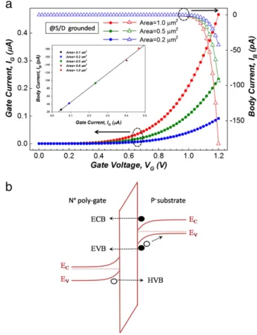
To examine the origin of additional carriers (hole) caused by the gate leakage current (IG),Fig. 3(a) illustrates the IGand IBversus gate
voltage (VG) for different N+poly-gate area (1μm2to 0.2μm2) while
the source/drain (S/D) is grounded. Clearly, the IBhas a significant
enhancement as the IGincreases, meaning that the source of IB is
strongly dependent on the IG. Furthermore, the linear relationship
between IBand IGis also obtained as shown in the inset ofFig. 3(a).
The IB–VGcurve inFig. 3(a) shows that the VGcorresponding to the
rapid increase of IBfor different N+poly-gate areas always locates
around 0.9 V. This indicates that additional carriers only can be generated under certain vertical electricalfield regardless of the poly-gate area.
It was proposed that the IGconsists of electron tunneling from the
conduction band (ECB), electron tunneling from the valence band (EVB), and hole tunneling from the valence band (HVB) as shown in
Fig. 3(b)[7]. In fact, the hole accumulation in the p−substrate has been explained due to EVB and HVB tunneling currents under a FB condition. However the EVB tunneling model was widely accepted to explain the LKE phenomenon because the HVB is typically very small for NMOS[5].
Fig. 1. The illustration of sample bending on the holder with curvature radius R = 30 mm.
Fig. 2. (a) Transfer characteristics for PD SOI n-MOSFETs under GB and FB operations. (b) The gm as a function of the gate voltage under the FB operation in the linear region (VD= 50 mV). IBis measured under the GB operation.
Fig. 3. (a) IG–VGand IB–VGcurves for different N+poly-gate areas. Inset displays the linear
relationship between IBand IGfor different N+poly-gate areas. (b) The schematic diagram
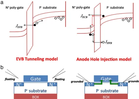
InFig. 4(a), the schematic band diagram of EVB shows that the electrons tunnel from the valence band of the Si substrate to the poly-gate conduction band under a sufficiently large vertical electric field. As a result, holes accumulate in the body due to thefloating body, which leads to a rise in the body potential. However, the other mechanism, that of AHI[8], also shown in theFig. 4(a), is also a possible model to explain the LKE. In AHI, when the gate oxide is thin enough, electrons can tunnel from the inversion layer to the poly-gate (anode) and generate hot holes by impact ionization in the poly depletion region. Then these hot holes can inject over or through the anode/oxide interface energy barrier and traverse the oxide layer to the body (cathode). Consequently, the HVB tunneling current becomes significant due to the increase of AHI tunneling current from the poly-gate to the p−substrate. Both mechanisms generate holes that accumulate in the body, but there are two key differences between the EVB tunneling and AHI model. One is the source of electrons: the electrons in the EVB tunneling model come from the band, but the source of electrons in the AHI model is from the conduction band. The other difference is that the intensity of the vertical electricfield in the EVB tunneling model is larger than that in the AHI model. This is because the VGin the EVB tunneling model
needs to be larger than the silicon band gap (1.1 V) to make the band energy level in the silicon substrate align with the gate conduction band[7]. Our experimental results that identify the rapid increase of IB
for different N+poly-gate areas located at around 0.9 V imply that the AHI model is more likely to be responsible for the GIFBE.
To further verify that the AHI model is the dominant mechanism of GIFBE, two operation conditions illustrated inFig. 4(b) are performed to distinguish the different sources of IG that result in hole
accumulation. We measured the IG and IB versus VGof the device
under S/Dfloating and grounded operations. The result under the S/D floating operation is shown inFig. 5, where it can be clearly observed that the gate leakage current becomes insignificant because the S/D cannot supply sufficient minority carriers (electrons) to the inversion layer. The IBis not evident (~ 0.1 pA) in this operation. On the contrary,
both currents show very pronounced increases under the S/D grounded operation. The results prove that the origin of GIFBE can be attributed to the electrons in the inversion layer, rather than the electron-hole pair separated in the valence band of the P−substrate. Therefore, the AHI model is the dominant mechanism responsible for GIFBE.
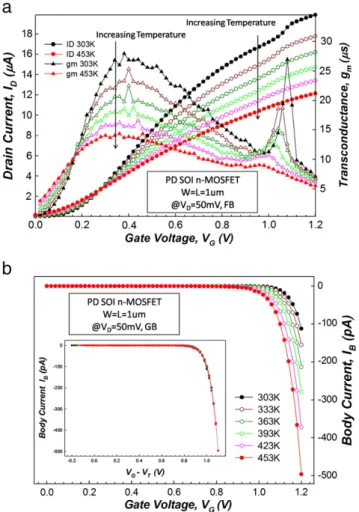
The second gm peak introduced inFig. 2was also analyzed as a function of temperature in the range from 303 K to 453 K.Fig. 6(a) shows that the second peak amplitude becomes smaller and shifts left as the temperature increases. This reduction is ascribed to an increase in recombination rate in the source and drain junctions as temper-ature increases[9]. To investigate the second gm peak shift, the IB–VG
curve as a function of temperature was also measured and shown in
Fig. 6(b) for comparison. It shows that the left shift trend of IBagainst
temperature is similar to that of the second gm peak. However, IBhas
no significant change after a VTcorrection for different temperatures,
as shown in the insert of Fig. 6(b). The results provide further evidence that hole injection from the anode is direct tunneling, because it is independent of temperature.
To further investigate the influence of tensile strain on GIFBE,
Fig. 7(a) presents the transfer characteristics of the SOI n-MOSFET under the GB operation with mechanical strain, as compared to the un-strained device (without strain). The result indicates that the Idlinand gm improve 3.0% and 3.4%, respectively. The enhancement
can be attributed to the reduction in the effective mass and intervalley scattering caused by the tensile strain effect [10]. In addition, the transfer characteristics of the devices under the FB operation both with and without tensile mechanical strain are
Fig. 4. The schematic diagrams of (a) EVB tunneling and AHI models for an ultra thin gate oxide of PD SOI n-MOSFET and (b) the device under S/Dfloating and grounded operations. Fig. 5. IG–VGand IB–VGcharacteristics for PD SOI n-MOSFET under S/Dfloating and
shown inFig. 7(b). Under the mechanical strain, the position of GIFBE shifts toward a lower VGand the magnitude of second gm
peak increases obviously. Furthermore, after the second peak, the gm for the strained device recovers its initial trend (under the GB operation trend), as compared to the un-strained device.
To realize the influence of the strain on the second gm peak clearly, the IGand IB versus VGwith and without mechanical strain were
measured in Fig. 8. It shows that the left shift trend of IB under
mechanical strain is similar to that of the second gm peak. Besides, the IG decreases slightly under the mechanical strain. This opposing
reduction is due to the strain-induced change in the conduction band offset between Si and the SiO2 gate dielectric[3].
Based on the AHI model, the IB generally decreases as the IG
decreases. However,Fig. 8indicates that even if the IGdecreases under
the mechanical strain, the IBstill increases significantly. This unusual
result is mainly related to the narrowing band gap induced by the mechanical strain effect[11]–[13]. Because the impact ionization rate is exponential to the energy band gap, the narrowing band gap causes more additional holes to be generated in the poly depletion region, leading to the increase of IB and a significant second gm peak in
strained SOI devices. Besides, after the second peak, the gm for the strained device recovers its initial trend. This implies that the enhanced IBcauses the body potential to reach the junction diode
threshold voltage. Therefore, for the strained device, holes cannot further accumulate in the body, resulting in the gm recovery after the second peak[4].
4. Conclusion
In this work, wefirst demonstrate that the EVB tunneling model is not the dominant mechanism for the GIFBE. When oxide thickness is reduced to only 12 Å, both IGand IBare insignificant under the S/D floating
operation. Therefore, the GIFBE can be attributed to the electrons of the inversion layer supplied from the S/D. This result indicates that the increase of HVB tunneling current induced by AHI is the dominant mechanism responsible for the GIFBE. By analyzing IBas a function of Fig. 6. (a) Transfer characteristics as a function of temperature varying from 303 to
453 K under the FB operation and (b) IB–VGcharacteristics of the PD SOI n-MOSFET
with body-contact for different temperatures. The inset shows the IB–VGafter a VT
correction, where the VTis obtained from linear extrapolation from the gmmax.
Fig. 7. Transfer characteristics for PD SOI n-MOSFETs with and without mechanical strain under (a) the GB operation and (b) the FB operation.
Fig. 8. IG–VG and IB–VGcharacteristics for PD SOI n-MOSFET with and without
mechanical strain. The inset shows the schematic diagrams of the AHI model under mechanical strain.
temperature, we also prove that the hole current (IB) is direct tunneling
from the poly-gate. This is because IBis independent of temperature after
a VTcorrection. Based on the AHI model, it was found that the tensile
strain has a strong impact on the GIFBE. This is owing to the band gap narrowing induced by the strain effect in the poly-gate.
Acknowledgments
Part of the work was performed at the United Microelectronics Corporation. The work was supported by the National Science Council under Contract NSC-98-3114-M-110-001, and NSC-97-2112-M-110-009-MY3.
References
[1] J.C. Sturm, K. Tokunaga, J.P. Colinge, IEEE Electron Device Lett. 9 (1988) 460.
[2] T. Ghani, K. Mistry, P. Packan, S. Thompson, Stealer M, Tyagi S, VLSI Tech Dig, 2000 174.
[3] W. Zhao, A. Seabaugh, V. Adams, D. Jovanovic, B. Winstead, IEEE Electron Device Lett. 26 (2005) 410.
[4] A. Mercha, J.M. Rafi, E. Simoen, E. Augendre, C. Claeys, IEEE Trans. Electron Dev. 50 (2003) 1675.
[5] P.G.D. Agopian, J.A. Martino, E. Simoen, C. Claeys, Microelectron 38 (2007) 114. [6] M. Cassé, J. Pretet, S. Cristoloveanu, T. Poiroux, C. Fenouillet-Beranger, F. Fmleux, C.
Raynaud, G. Reimbold, Solid-State Electronics 48 (2004) 1243. [7] W.-C. Lee, C. Hu, IEEE Trans. Electron Devices 48 (2001) 1366. [8] K.F. Schuegraf, C. Hu, IEEE Trans. Electron Devices 41 (1994) 761.
[9] L. Vancaillie, V. Kilchytska, P. Delatte, L. Demeus, H. Matsuhashi, F. Ichikawa, D. Flandre, IEEE Int. SOI Conf. (2003) 78.
[10] S.E. Thompson, M. Armstrong, C. Auth, S. Cea, R. Chau, G. Glass, IEEE Electron Device Lett. 25 (2004) 191.
[11] F.A.I.R. RB, J. Appl. Phys. 50 (1979) 860.
[12] T. Irisawa, T. Numata, N. Sugiyama, S. Takagi, IEEE Trans Electron Dev. 52 (2005) 993.
[13] Y.J. Kuo, T.C. Chang, P.H. Yeh, S.C. Chen, C.H. Dai, C.H. Chao, Thin Solid Films 517 (2009) 1715.