Ion-Implantation Techniques
Shih-Yung Huang,aRay-Hua Horng,b,*
,zHao-Chung Kuo,cand Dong-Sing Wuua a
Department of Materials Science and Engineering and bInstitute of Precision Engineering, National Chung Hsing University, Taichung, Taiwan 402, Republic of China
c
Institute of Electro-optical Engineering, National Chiao Tung University, Hsinchu, Taiwan 300, Republic of China
The InGaN-based green resonant-cavity light-emitting diodes共RCLEDs兲 have been fabricated using hydrogen ion-implantation and laser liftoff techniques. The RCLEDs structure consisted of an InGaN/GaN multiple-quantum-well active layer between the top共5 pairs兲 and bottom 共7.5 pairs兲 dielectric TiO2/SiO2distributed Bragg reflectors with optical reflectance of 85% and 99.9%,
respectively. The insulation layers of the RCLEDs with and without H+ implantation were formed by the hydrogen
ion-implantation layers of 1⫻ 1014ions/cm2concentration and SiO
2film, respectively. The corresponding forward turn-on voltage at
0.6 kA/cm2dc current density injection were about⬃4.58 V and ⬃4.55 V for the RCLEDs with and without H+implantation.
The light output intensity of the RCLEDs with H+implantation is higher by a factor of 1.4 as compared to that of the similar
structure without H+implantation at a current density of 0.6 kA/cm2. The directionality of RCLEDs with H+implantation is
superior to that of RCLEDs without H+implantation.
© 2007 The Electrochemical Society. 关DOI: 10.1149/1.2778860兴 All rights reserved.
Manuscript submitted June 5, 2007; revised manuscript received July 23, 2007. Available electronically September 14, 2007.
Gallium nitride共GaN兲-based materials have attracted much at-tention due to their wide bandgaps. It has become the dominant semiconductor system operating in the visible to ultraviolet range.1,2 Over these latter years, resonant-cavity light-emitting diodes 共RCLEDs兲3-6
have been developed for optical communication along plastic optical fibers共POFs兲, optical interconnect, optical signal pro-cessing, and optical neutral network because the RCLEDs present several advantages over conventional light-emitting diodes共LEDs兲, such as a narrow spectral linewidth, better emission directionality, high output power, and an enhanced light extraction efficiency.7The minimum attenuation windows of the POFs are 510 nm and 570 nm.8Obviously, InGaN-based semiconductor devices are suit-able for these wavelengths. It is well known that the RCLEDs op-erating in the wavelength of red and infrared light have been achieved. As concerning the InGaN-based green RCLEDs are sel-dom reported.9,10Therefore, we have studied this subject and dem-onstrate that the InGaN-based green RCLED devices may be attain-able.
Generally, an active region of the RCLED devices was placed in two distributed Bragg reflector共DBR兲 mirrors that form a Fabry– Perot cavity. Such a resonant cavity can be used to enhance the spontaneous emission at the resonant wavelength, while off-resonance emission would be constrained.11,12The typical structures of the DBRs is made of alternate layers of low-index and high-index materials, and the thickness of optical film must conform to the quarter wavelength. It can produce the maximum reflectivity in the resonant wavelength. In order to obtain the RCLEDs with superior directional and high light extraction efficiency, the hydrogen ion 共H+兲 is implanted into the p-GaN layers results in a confinement of
the current flowing and light-emitting direction. In contrast to con-ventional LEDs and vertical-cavity surface emitting lasers, the ion-implantation techniques based on nitride compound semiconductors are at their infancy. However, this is a way to acquire RCLEDs with superior performances. In this paper, the InGaN-based green RCLED with H+implantation on Si substrate is produced by using a
laser liftoff process. The thin multiple quantum well共MQW兲 active regions sandwiched in between two DBR mirrors that form a Fabry– Perot cavity. The multipair dielectric TiO2/SiO2films were used as
the top and bottom DBRs. Details of the optical and electrical prop-erties of InGaN-based green RCLEDs with H+implantation are de-scribed next.
Experimental
The InGaN-based green LED structure was grown on c-plane-oriented sapphire substrates by the metallorganic chemical vapor deposition system. The epitaxial structure comprises a 30 nm thick GaN nucleation layer, a 4m thick Si-doped GaN n-cladding layer, MQW active region, and a Mg-doped p-type cap layer. The MQW active region consists of five periods of 3 nm thick In0.22Ga0.78N well layers and 10 nm thick GaN barrier layers. Prior to device fabrication, the epilayers were implanted by H+. The deep proton
implantation process is as follows: a Si3N4film is deposited on the p–GaN layers and confined light output aperture is masked by pho-toresist using common photolithography. The epi layer is bombarded by H+in 120 keV acceleration energies and 1⫻ 1014ions/cm2 con-centration. Ion-implantation depth is selected to reach high damage levels from the epi layer surface down to the MQW active regions共 ⬃0.3 m deep兲. The 356 ⫻ 356 m p-mesa was etched by the re-active ion-etching system. A current spreading layer was formed using a 200 nm thick layer of high-conductivity transparent indium-tin oxide film onto the mesa by E-beam evaporation system and then thermal annealed at 550°C in N2 ambient for 5 min. The p- and n-contact pads were also formed using Cr/Au layers. A total of five pairs of TiO2/SiO2DBRs were evaporated as the top mirrors using
the electron beam evaporation system. The TiO2 and SiO2 layer thicknesses were estimated for simulations via an in situ optical reflectance trace and quartz monitor. Then, the LEDs epi layer was bonded to a temporary glass substrate using an adhesive, then sub-jected to the laser liftoff共LLO兲 process. A UV laser was irradiated from the back surface of the sapphire substrate. The GaN was lo-cally heated and dissociated close to the sapphire/GaN interface. After the entire wafer was illuminated by the laser beam, the sap-phire substrate was separated from the RCLEDs structure. A diluted HCl solution was used to dissolve the residual Ga droplets on the exposed GaN surface. Subsequently, 7.5 pairs of TiO2/SiO2DBRs were evaporated as the bottom mirrors. A GaN epi layer with top and bottom DBRs structures was then fused to the silicon substrate using a wafer bonding system with a conductive adhesive layer. The bonding process was performed at 100°C for 20 min under a pres-sure of 15 psi.
Finally, the sample was removed from the temporary glass sub-strate and a complete RCLED structure with H+ implantation on
*E-mail: [email protected]
z
silicon substrate specimen was obtained. For comparison, a RCLED without H+ implantation was also fabricated. The only difference was to adopt the SiO2 film as insulation layers from the RCLEDs
with H+ implantation. The chips were mounted on gold-coater
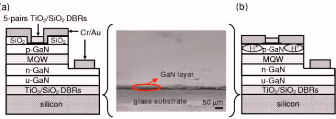
TO-46 cans and packaged to protect the surface. A cross-sectional diagram of two types of RCLEDs with and without H+implantation on Si substrate is shown in Fig. 1. A scanning electron microscopy 共SEM兲 micrograph of the GaN surface after LLO process are also shown in Fig. 1.
The current-voltage 共I-V兲 characteristics of the InGaN-based green RCLEDs were measured using an Agilent 4155B semiconduc-tor parameter analyzer at room temperature. Electroluminescence 共EL兲 was measured with an ARC spectrometer and Si photodetector at room temperature. Communications experiments were carried out in order to demonstrate that the RCLEDs admit for transmission by an Agilent 83480A digital communications signal analyzer. The emission light of the chips was measured from the top of the bare chip without encapsulating into epoxy.
Results and Discussion
The images of the GaN surface with and without Ga droplets are shown in Fig. 2a and b, respectively. Figure 2a shows the residual Ga droplets at the GaN film/sapphire interface. This phenomenon is the GaN to generate thermal decomposition by laser irradiation, the relation as follows13
GaN→ Ga + 1
2 N2共gas兲 关1兴
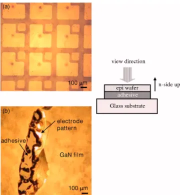
The GaN can be decomposed into gaseous nitrogen and gallium droplets after laser irradiation. These residual Ga droplets were dis-solved on the exposed GaN surface by a diluted HCl solution. Fig-ure 2b showed the GaN surface after Ga droplets were removed. It is necessary to remove the Ga droplets due to the reflectivity require-ment of the following bottom mirror. The plane view optical micro-scope images of the GaN surface without and with crack after the LLO process are shown in Fig. 3a and b, respectively. An acceptable surface is shown in Fig. 3a. The GaN film has neither lateral crack-ing nor film breakage at a pulse energy of⬃0.7 J/cm2. This result
could be attributed to the fact that the laser beam has enough energy to penetrate into the sapphire substrates without the formation of stresses and cracking of the thin film. However, the GaN film was broken at higher pulse energies共0.9 J/cm2兲 as shown in Fig. 3b. It
was found that the exposed adhesive and the electrode pattern was face up after the LLO process. Because the speed of laser beam is very fast共several nanoseconds per pulse兲, it results in the generation of a vaporization pressure of N2. When the vaporization pressure is
too great, the GaN film may swell and result in the epi layer crack-ing. This point is also reported by Tavernier and Clark.14
Figure 4 shows an atomic-force-microscopy image of the GaN surface without Ga droplets after wet etching. The root-mean-square surface roughness of the GaN was⬃23 nm in an area of 25 m2. This degree of GaN surface roughness will not result in the emission light scattering for our specimen. Because the emission wavelength range共510–530 nm兲 of the specimen is much greater than the GaN
surface roughness after wet etching, and therefore the light from the specimen had penetrated directly through the roughness surface of the GaN. However, the roughness degree of the GaN surface after the LLO process as compared to the roughness degree for the speci-men before the LLO process was larger due to the thermal decom-position at the GaN film/sapphire interface.15Figure 5 shows the photoluminescence 共PL兲 spectra of the GaN surface without Ga droplets before and after the LLO process. The peak wavelength and full width at half maximum共fwhm兲 of the PL for the GaN film after the LLO process is at 372 nm and 9.03 nm, respectively. Corre-spondingly, the peak wavelength and fwhm of the PL for the GaN film before the LLO process is at⬃371 nm and ⬃9 nm, respec-tively. The optical properties are almost the same for the GaN films before and after the LLO process. Obviously, the free-standing GaN epi layer is not destroyed by the LLO process.16,17
Figure 6 shows the reflectivity spectra of the top 5 pairs and bottom 7.5 pairs of TiO2/SiO2dielectric DBRs. It was found that the
Figure 1. 共Color online兲 Schematic
dia-grams of共a兲 the RCLEDs without H+
im-plantation and共b兲 the RCLEDs with H+
implantation on silicon substrates. The in-set shows a SEM micrograph of the GaN surface after the laser liftoff process.
Figure 2.共Color online兲 Photograph images of the GaN surface 共a兲 with Ga
high reflectivity of top and bottom DBRs were very close to the target wavelength at 525 nm. They also presented a broad stop-band width of⬃100 nm as the reflectivity of above 80%. Furthermore, the reflectivity of the top five pairs of TiO2/SiO2DBRs共85%兲 was
designed lower than that of the bottom dielectric DBRs共99.9%兲 at 525 nm, which forms a mirror of semitransmittance and semireflec-tivity. The field-emission scanning electron microscopy共FESEM兲 image of 7.5 pairs of dielectric DBRs are also shown in the inset of Fig. 6. The thickness of the TiO2 and SiO2is 40 nm and 95 nm, respectively. The result indicated that the thickness of DBRs is con-forming to the designed thickness.
The EL spectra from the nonencapsulated RCLEDs with and without H+ implantation at 0.6 kA/cm2forward operation current
density injections are shown in Fig. 7, in which the emission peak wavelength is located at 525 nm. The main peak wavelength reflec-tivity of the DBRs shows good agreement with the peak wavelength of the EL spectrum. The optical properties of these devices have been obtained by optical detector and set above the surface of the sample within an angular view of⬃10° to measure the top emission light. It was found that the emission spectra from the RCLEDs with and without H+implantation were periodically modulated with
sev-eral narrow resonant wavelength peaks. This phenomenon indicates that the modulation of the EL spectra is the result of the Fabry–Perot cavity effect. However, the EL intensity of the RCLEDs with H+
implantation is higher than that of the RCLEDs without H+ implan-tation. This is because the H+implantation results in the high carrier
Figure 3.共Color online兲 Plane view optical microscope images of the GaN
surfaces共a兲 without breakage and 共b兲 with breakage after laser liftoff.
Figure 4.共Color online兲 Atomic force microscopy of the GaN surface
with-out Ga droplets after wet etching.
Figure 5. Photoluminescence spectra of the GaN on sapphire and GaN
trans-ferred onto silica substrate.
Figure 6. Reflectivity spectra of the top 5 pairs and bottom 7.5 pairs of
TiO2/SiO2dielectric DBRs. The inset presents a FESEM image of 7.5 pairs
of dielectric DBRs.
Figure 7. EL spectra of RCLEDs with and without H+implantation on Si
substrates at 0.6 kA/cm2current density injection. The forward I-V
charac-teristics of RCLEDs with and without H+implantation at the same current
injection efficiency. It produced the electrons combining with holes effectively and resulted in more spontaneous emission light from light aperture beam.18The reabsorbed light by the p-electrode was also reduced. On the contrary, the spontaneous emission light of the RCLEDs without H+ implantation specimen was absorbed by the
metal electrode on the p-GaN layers. The forward I-V of the RCLEDs with and without H+ implantation are also shown in the inset of Fig. 7. The corresponding forward turn-on voltage at 0.6 kA/cm2 dc current density injection was determined ⬃4.58 V
and ⬃4.55 V, respectively. The result indicated that the RCLEDs with H+implantation structure have similar I-V as compared to that
with the RCLEDs without H+ implantation.
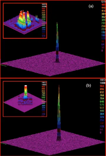
Figure 8 shows the EL intensity of the RCLEDs with and without H+implantation as a function of injection current density at room
temperature. Obviously, the EL intensity of the RCLEDs with H+
implantation is higher by a factor of 1.4 as compared to that with the RCLEDs without H+implantation under 0.6 kA/cm2injection cur-rent density. The improvement of optical output is mainly attributed to the greater emission directionality by H+implant into the p-GaN layers to confine the current flow route, and the light emitting was not absorbed by the metal electrode on the p-GaN layers. Figure 9 shows the far-field patterns of the RCLEDs with and without H+
implantation at 0.6 kA/cm2current density injection by the charge
coupled device 共CCD兲. The far-field patterns were measured by placing a polarizer in front of the light emission beam of the RCLEDs. It was found that the light output patterns of the RCLEDs with and without H+ implantation were a nearly Gaussian
distribu-tion. The RCLEDs with H+ implantation have much higher light-emission intensity than that of the RCLEDs without H+
implanta-tion. The far-field patterns of both types of RCLEDs without placing a polarizer for light distribution condition were also measured and are shown in the insets of Fig. 9. Obviously, the directionality of RCLEDs with H+ implantation performs superior to that of the
RCLEDs without H+ implantation. From the device structure as shown in Fig. 1, it can be found that the current can spread into the MQW for the RCLEDs without H+implantation, but the current can
be confined to below aperture for the RCLEDs with H+
implanta-tion. Thus, some light can escape from the edge for the RCLEDs without H+implantation. However, H+implantation restricts current
flows to the area below aperture. There is less light emission from the edge. These results indicated that the insulation layer can effec-tively control the light-emission route by the H+implantation man-ner.
In the above description, the RCLEDs with H+ implantation
present better emission directionality and enhanced light extraction efficiency as compared to the RCLEDs without H+ implantation.
This suggests that the greater intensity can result in higher output power. However, the output power is indeed important to assess the
benefit of the RCLED fabricated by H+ implantation. It is
under-measured. By the way, some are mainly aimed at the RCLEDs with H+implantation structures in the content below. In order to
investi-gate the resonant-cavity effect on the light-emission of the RCLEDs, the angle-resolved EL measurements form RCLEDs with H+ im-plantation sample, as shown in Fig. 10. In the plot, the 0° of the EL spectrum corresponds to the emitted normal to the surface. We clearly observed the EL peak wavelength of the RCLEDs with H+
implantation was blueshift and the EL intensity weakens from 519 to 515 nm when detector angle diverged from the emitted nor-mal to the surface. The result is a typical resonant-cavity effect and agreement with a previous report on nitride-based RCLEDs.19We demonstrate this through the following relation
0
=
冑
1 −冉
sin2共兲
ncav2
冊
关2兴where is the angle with regard to the emitted normal to the surface, and 0are the EL peak wavelength at and normal to the
sur-face, and ncavis the refractive index of the resonant cavity. If ncavis
a constant, the value ofdecreased as the value of increase. An image of the RCLEDs共0° resolved兲 with H+ implantation is also shown in Fig. 10. The emitted light is clearly confined to the device center. It is important to evaluate the communication function for the RCLEDs with H+ implantation. Figure 11 shows the eye
dia-gram of the RCLEDs with H+implantation at a 1.3 kA/cm2current
Figure 8. EL intensity as a function of injection current density of RCLEDs
with and without H+implantation.
Figure 9. 共Color online兲 Far-field patterns of the RCLEDs 共a兲 without H+
implantation and共b兲 with H+implantation by the CCD with placing a
polar-izer in front of light-emission beam of the RCLEDs. Far-field patterns of both types of RCLEDs without placing a polarizer are also shown in the inset.
density injection for 100 MHz communication experiments. It was found that the eye diagram shows the rise and fall time共20–80%兲 being 4.40 ns and 4 ns, respectively. Furthermore, the eye diagram has a good open eye. This result indicated that such RCLEDs are
The characteristics of the InGaN-based green RCLEDs operating at 525 nm by using H+ implantation techniques have been
de-scribed. The light output intensity at 0.6 kA/cm2 of the RCLEDs
with H+ implantation was enhanced by a factor of 1.4 due to the greater emission directionality by H+implant into the p-GaN layers
to confine the current flow route, and the light emitting was not absorbed by the metal electrode on the p-GaN layers. The light-emission directionality and current confinement effect of the RCLEDs with H+ implantation is better than that of the RCLEDs
insulated by SiO2. Hence, the RCLEDs are not only suitable for POF communication system, but could replace the standard LEDs in many applications.
Acknowledgments
This work was supported by the National Science Council and Ministry of Education of the Republic of China under contract no. NSC-95-2221-E-005-147 and ATU plan, respectively.
National Chung Hsing University assisted in meeting the publication charges of this article.
References
1. S. Nakamura, T. Mukai, and M. Senoh, Appl. Phys. Lett., 64, 1687共1994兲. 2. S. Nakamura, M. Senoh, N. Iwasa, and S. Nagahama, Jpn. J. Appl. Phys., Part 2,
34, L797共1995兲.
3. Y. K. Song, H. Zhou, M. Diagne, I. Ozden, A. Vertikov, and M. R. Krames, Appl.
Phys. Lett., 74, 3441共1999兲.
4. M. Pessa, M. Guina, M. Dumitrescu, I. Hirvonen, M. Saarinen, L. Toikkanen, and N. Xiang, Semicond. Sci. Technol., 17, R1共2002兲.
5. P. Royo, R. P. Stanley, and M. Ilegems, J. Appl. Phys., 90, 283共2001兲. 6. R. H. Birkner, J. Kaiser, W. Elsäßer, and C. Jung, Appl. Phys. B: Lasers Opt., 79,
963共2004兲.
7. H. Benisty, H. de Neve, and C. Weisbuch, IEEE J. Quantum Electron., 34, 1632 共1998兲.
8. F. Calle, F. B. Naranjo, S. Fernández, M. A. Sánchez-García, E. Calleja, and E. Muñoz, Phys. Status Solidi A, 192, 277共2002兲.
9. Y. K. Song, M. Diagne, H. Zhou, and A. V. Nurmikkoa, Appl. Phys. Lett., 77, 1744 共2000兲.
10. F. B. Naranjo, S. Fernández, M. A. Sánchez-García, F. Calle, and E. Calleja, Appl.
Phys. Lett., 80, 2198共2002兲.
11. M. Selim Ünlü and S. Strite, J. Appl. Phys., 78, 607共1995兲.
12. H. Benisty, H. de Neve, and C. Weisbuch, IEEE J. Quantum Electron., 34, 1612 共1998兲.
13. W. S. Wong, T. Sands, N. W. Cheung, M. Kneissl, D. P. Bour, P. Mei, L. T. Romano, and N. M. Johnson, Appl. Phys. Lett., 75, 1360共1999兲.
14. P. R. Tavernier and D. R. Clarke, J. Appl. Phys., 89, 1527共2001兲.
15. C. F. Chu, F. I. Lai, J. T. Chu, C. C. Yu, C. F. Lin, H. C. Kuo, and S. C. Wang, J.
Appl. Phys., 95, 3916共2004兲.
16. P. Perlin, L. Mattos, N. A. Shapiro, J. Kruger, W. S. Wong, T. Sands, N. W. Cheung, and E. R. Weber, J. Appl. Phys., 85, 2385共1999兲.
17. W. S. Wong, Y. Cho, E. R. Weber, T. Sands, K. M. Yu, J. Krüger, A. B. Wengrow, and N. W. Cheung, Appl. Phys. Lett., 75, 1887共1999兲.
18. M. M. Dumitrescu, M. J. Saarinen, M. D. Guina, and M. V. Pessa, IEEE J. Sel. Top.
Quantum Electron., 8, 219共2002兲.
19. P. de Mierry, J. M. Bethoux, H. P. D. Schenk, M. Vaille, E. Feltin, B. Beaumont, M. Leroux, S. Dalmasso, and P. Gibart, Phys. Status Solidi A, 192, 335共2002兲.
Figure 10. 共Color online兲 Angle-resolved EL spectra of the RCLEDs with
H+implantation. The inset presents the photograph image of the RCLEDs
with H+implantation at 0° direction.
Figure 11.共Color online兲 Eye diagram of the RCLEDs with H+implantation
at 1.3 kA/cm2 current density injection for 100 MHz communication