Transition from flip chip solder joint to 3D IC microbump: Its effect
on microstructure anisotropy
K.N. Tu
a,⇑, Hsiang-Yao Hsiao
b, Chih Chen
b aDepartment of Materials Science and Engineering, University of California at Los Angeles, Los Angeles, CA 90095-1595, USA b
Department of Materials Science and Engineering, National Chiao Tung University, Hsinchu, Taiwan, ROC
a r t i c l e
i n f o
Article history: Received 23 April 2012
Received in revised form 23 July 2012 Accepted 24 July 2012
Available online 1 September 2012
a b s t r a c t
As microelectronic industry develops 3D IC on the basis of through-Si-vias (TSV) technology, the process-ing and reliability of microbumps, which are used to interconnect the stackprocess-ing chips, is beprocess-ing actively investigated. Due to the reduction in size of microbumps, the diameter is about one order of magnitude smaller than that of flip chip solder joints, and the volume is 1000 times smaller. Its microstructure and in turn its properties will be anisotropic because the number of grains in a microbump becomes very small. Its statistical failure will have a wide distribution because of anisotropy, including early failure. This review addresses this issue and the remedy.
Ó 2012 Elsevier Ltd. All rights reserved.
1. Introduction
As the trend of miniaturization of large-scale-integration of cir-cuits on Si chip technology is approaching the limit of Moore’s law, microelectronic industry has been looking for ways to overcome or to extend the limit. One of the ways is to turn to 3D IC by combin-ing chip technology and packagcombin-ing technology. This is because the Moore’s law for packaging technology, assuming there is one, has not reached its limit yet. If we just consider the diameter of solder joints, in today’s flip chip technology, the diameter is about 100
l
m, and the diameter of microbumps in 3D IC is now about 20l
m. It is possible that the solder joint diameter can be reduced to 1l
m, thus there is ample room in the near future for the pack-aging technology to advance.In packaging technology, whether we have systems in packag-ing (SIP) or systems on chip (SOC), they are 3-dimensional struc-tures. To stack Si chips, the industry is seriously developing the through-Si-via (TSV) technology and microbump technology
[1,2]. The latter is used to join the vias between two TSV chips in stacking. Owing to the change in dimension and in geometry, the reliability issues in 3D IC packaging will be different from those in flip chip. The change in dimension is because the diameter of via is about 10
l
m, so does the diameter of microbumps, and the change in geometer is because of 3D integration. Before we address the new reliability challenges, we consider the following five gen-eral questions regarding the transition from flip chip to 3D IC.The first is that 3D IC by using wire bonding technology is much cheaper than that by using TSV plus microbumps, so why should
we develop the latter? This question has been asked before when microelectronic industry was trying to develop flip chip technology since at that time wire bonding was widely used and was much cheaper. The answer is because of the number of I/O on the chip; in wire bonding the number is proportional to the linear dimension of the peripheral of the chip, which is 4l if l is the length of the edge of a chip. Typically, it is limited to about 400 wires or 400 I/O. On the other hand, in flip chip, the number of solder bumps will be proportional to the area of chip, l2, so the number of I/O can be
up to 10,000. The same argument applies to 3D IC; if a low number of I/O can serve the purpose, we use wire bonding. But if the device needs a large number of I/O, we have to use TSV and microbumps. The second question is about joule heating; it will be very seri-ous, so how to reduce it or conduct it away[3–6]? Upto now, there is no proven solution to this fundamental problem. While Cu TSV is used for electrical interconnect between stacking chips in 3D IC, some of them can be used for heat conduction since Cu is a good electrical and thermal conductor. Thus, we can have two kinds of TSV; one kind is electrical TSV and the other kind is thermal TSV. The latter will require thermal contacts. Since thermal conduction depends on temperature gradient, thermomigration can occur and it will become important in the reliability of thermal contacts as well as in thermal interfacial materials (TIM). It is worth mention-ing that a temperature difference of only 1 °C across a thickness of 10
l
m results in a temperature gradient of 1000 °C/cm, which is known to have caused thermomigration in Pb-free solders at the operation temperature of 100 °C[7–10]. On the other hand, a prac-tical approach to deal with the heat problem is to begin with a stacking of only two to three Si chips so that the problem will not be too serious. We need to learn to overcome it step by step be-fore we jump to the stacking of a large number of chips.0026-2714/$ - see front matter Ó 2012 Elsevier Ltd. All rights reserved.
http://dx.doi.org/10.1016/j.microrel.2012.07.029 ⇑Corresponding author.
E-mail address:[email protected](K.N. Tu).
Contents lists available atSciVerse ScienceDirect
Microelectronics Reliability
The third question is while the size of microbump is reduced, the temperature and time of processing is not, for example, the temperature and time of reflow will be more or less the same as that used in processing flip chip solder joints. Then, what will be the consequence? The consequence is that the relative amount of intermetallic compound (IMC) formed between solder and un-der-bump-metallization (UBM) will be greatly increased[11–13]. Also this is because while we reduce the thickness of solder, we do not reduce the UBM thickness in proportion. The entire solder joint may transform completely to intermetallic. In the literature, this issue has been addressed[14,15]. Since the physical and reli-ability problems of IMC is not well known, more research and data on IMC will be needed in the near future.
The fourth question is about chip-packaging interaction. Whether or not it will be more serious in 3D IC than that in flip chip packaging? Chip-packaging interaction is due to different thermal expansion coefficients between the Si chip and the poly-mer-based packaging substrate. The flip chip solder joints join the two. The cyclic thermal stresses in device operation will be transmitted to the on-chip multi-layered interconnects through the solder joints, especially those joints at the corners of the chip. When SiO2was the dielectric layer on multi-layered Al
intercon-nects and when the solder was eutectic SnPb, the soft solder joints will absorb most of the stresses. Since SiO2 is rather hard and
strong, the reduced thermal stress did not cause cracking or di-lamination of the dielectric. However, when low k dielectric was introduced to form the Cu/low k multi-layered interconnect systems and when a harder Pb-free solder replaces the soft SnPb eutectic, most of the thermal stresses are transmitted to the mul-ti-layered interconnect and has caused cracking of the low k dielec-tric and breakdown of the Cu/low k interconnects[16,17]. Because of this reliability problem, microelectronic packaging industry has developed the so-called 2.5D IC technology, in which a passive TSV interposer is inserted between the active Si chip and the substrate
[12]. The thermal stress between the active Si chip and the inter-poser is much reduced because both are Si. Thus, we expect that the chip-packaging interaction in 3D IC is similarly reduced. How-ever, since joule heating is more serious in 3D IC, thermal stress re-mains a key concern.
The fifth question concerns the anisotropic properties of small solder joints. When the diameter is reduced by 10 times, from 100
l
m to 10l
m, the volume is reduced by 1000 times. Thus, if we consider an extreme case in which the grain size is as-sumed to be 10l
m, the microbump may have only one grain, but the flip chip solder joint will have 1000 grains. In the latter case, we can assume the properties of the solder joint to be iso-tropic because of the large number of grains, but in the former case, we cannot.Since Sn has a body-centered tetragonal crystal structure, it has anisotropic properties, for example, its conductivity is anisotropic. In transforming Sn to Cu–Sn or Ni–Sn intermetallic compound (IMC), the IMC has anisotropic crystal structure too[18,19]. This is a concern because it means that among a large number of micro-bumps on a TSV chip, the properties of each of the micromicro-bumps can be different. From the point of view of reliability, it could mean a wide distribution in failure statistics, so some microbumps could have early failure. Thus, it is important to control the microstruc-ture or the grains of every microbump on a TSV chip in order to have a uniform microstructure in all of them. However, there are hundreds or even thousands of microbumps on a TSV chip, how to do so is challenging.
In this review, we shall concentrate on the issue of IMC in microbumps and how to control their formation in order to have an oriented growth and in turn a uniform microstructure in all the microbumps.
2. Effect of size reduction of microbumps on Sn whisker formation
Fig. 1a is a schematic diagram of the cross-sectional view of half a microbump, consisting of a 10
l
m thick layer of Sn–Ag on a thick Cu UBM. To form a microbump, we shall flip one of them up-side down and join it to another one. Before joining, we reflow the sol-der to form a cap on the Cu.Fig. 1b is an SEM image of the solder cap after reflow and after storage at room temperature for a while. Whiskers of Sn formed on the cap surface. Since the spacing be-tween microbumps is small, one of the whiskers is shown to have bridged two neighboring microbumps and it could become an elec-trical short.It is known in lead-frame technology that the plating of a layer of Sn or SnCu as surface finish on lead-frames of Cu has often shown Sn whisker growth [20,21]. When the layer thickness of Sn or SnCu is about 10
l
m, it is about the optimal thickness for Sn whisker growth. The driving force of spontaneous Sn whiskerFig. 1. (a) A schematic diagram of the cross-sectional view of half a microbump, consisting of a 10lm thick layer of Sn–Ag on a thick Cu UBM. (b) SEM image of the solder cap after reflow and after storage at room temperature for a while. Whiskers of Sn formed on the cap surface. (c) SEM image of a very smooth surface after reflow and no whisker growth was found.
growth is due to room temperature reaction between Sn and Cu to form Cu6Sn5IMC in Sn, the compressive stress induced by IMC
for-mation is relaxed by the diffusion of Sn to grow a stress-free whis-ker on the finish surface. The compressive stress gradient in a Sn layer of about 10
l
m thick is most effective for the stress migration in Sn whisker growth. On the other hand, in Pb-free flip chip solder joints of 100l
m on Cu UBM, very few Sn whiskers have been observed.To prevent Sn whisker growth on microbumps, a diffusion bar-rier layer of Ni is plated between the Cu and the Pb-free to prevent the Cu–Sn reaction.Fig. 1c shows the SEM image of a very smooth surface after reflow and no whisker growth was found. While the intermediate layer of Ni has prevented Cu6Sn5 formation and Sn
whisker growth, it nevertheless has made the microbump more brittle.
3. Effect of size reduction of microbumps on IMC formation and transformation
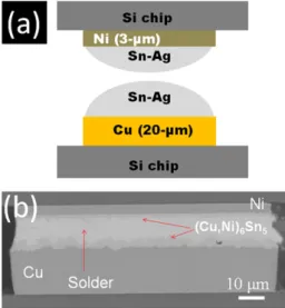
Fig. 2a is a schematic diagram of the cross-sectional view of forming a microbump by joining the upper half and the lower half of the half-structure depicted inFig. 1a. On IMC formation in such a microbump, we shall consider two issues which are not found in flip chip solder joints. Since the physical spacing between the upper and lower UBMs across a microbump is small or the physical spacing between the two solder/UBM interfaces is just about 10
l
m, the first question we ask is that how long does it take to al-low the IMC scallops growing from the upper side and from the lower side to touch each other. In other words, how long will it take to grow the average scallops to 5l
m in radius? This question is important in the sense that when scallops touch each other, the vertical dimension of the microbump is fixed. Subsequently, if any force tends to change the dimension, stress will be induced. In addition, when the scallops of Cu6Sn5stop growing, the growthof Cu3Sn between Cu6Sn5 and Cu will become fast. Since the
growth of Cu3Sn will lead to Kirkendall void formation[22], this
is a reliability concern, especially when the supply of Cu is plenty. The second question we ask is what will be the chemical inter-action between the two interfaces? Due to the small spacing be-tween them, atomic diffusion takes very little time to go from one side of the solder/UBM interface to the other side in the molten
state as well as in the solid state. The two interfaces in a micro-bump can communicate with each other much faster than those in flip chip solder joints.
To answer the first question, we recall that the growth rate of Cu6Sn5scallops in the reaction between eutectic SnPb and Cu at
temperature around 200 °C has been measured [23], and it will take about 30 min to grow hemispherical scallops of 5
l
m in ra-dius. If we assume this rate for microbumps, a longer annealing will lead to fast growth of the Cu3Sn phase.To answer the second question on the interaction between the two interfaces across the microbump, it can be seen clearly if we have Ni UBM on one side and Cu UBM on the other side. When Ni diffuses to the other side and vice versa, we can detect the inter-action directly due to the formation of ternary IMC. What will hap-pen in IMC formation is that the ternary SnCuNi compound is more stable than the binary IMC of SnCu or SnNi, so we expect ternary IMC to form on both interfaces. Furthermore, (Ni, Cu)3Sn4is less
stable than (Cu, Ni)6Sn5, so the latter will be the dominant ternary
IMC to form in microbumps, provided that both Cu and Ni are available. Thus even if (Ni, Cu)3Sn4forms first on the Ni UBM side,
it will transform to (Cu, Ni)6Sn5later.Fig. 2b is a cross-sectional
SEM image of a microbump which has had Ni UBM on one side and Cu UBM on the other side. Upper reflow, we found (Cu, Ni)6Sn5
on both sides, and it indicates the interaction between the two sides of the microbump.
The interaction is affected by the asymmetry of the microstruc-ture across the microbump. However, even if the design of the microstructure is symmetrical, it becomes asymmetrical when the device is powered because the electric current flow across the microbump is not symmetrical due to the anode and the cath-ode. Electromigration induced phase change will be asymmetrical; it is different between the anode and the cathode of the solder joint. Actually, electromigration will accelerate the IMC formation at the anode. The effect of electromigration on IMC formation in microbumps will not be covered in this review.
4. The control formation of oriented IMC in microbumps The number of grains in the Pb-free microbump before IMC for-mation as well as grains in the IMC after forfor-mation will be small, may be just a few grains, so we expect anisotropic behaviors. It is known that the diffusion of Cu and Ni in Sn is anisotropic, the diffusivity along the c-axis is about two to three orders of magni-tude faster than that along the a- and b-axis[24,25]. Thus the for-mation of IMC on a c-axis oriented Sn grain will be much faster than that on a-axis or b-axis oriented Sn grain[26]. Due to such anisotropic behavior, the grain orientation and the distribution of grain orientation in all the microbumps on a TSV chip are of con-cern. We ask whether or not we can control the orientation of the small number of Sn grains as well as the IMC grains in micro-bumps. The answer is yes and it can be done; we start from the control of grains in Cu UBM by forming (1 1 1) oriented nano-twins in the Cu.
The crystal structure of a face-centered-cubic metal such as Cu can be represented by a stacking of (1 1 1) planes in the sequence of ABCABC. When an error of stacking occurs and changes the stack-ing to ABCACBA, where the middle plane of A is a mirror of atomic planes on both sides, a twin is formed. The stacking error increases the internal energy of the crystal only slightly because each atom in the twin plane still has 12 closely packed nearest neighbors, thus twin is considered as a coherent planar defect of low energy. The energy increase is of the order of a stacking fault. Copper has a low stacking fault energy and twin energy, so even an ordinary piece of bulk Cu tends to have micro-twins, meaning the twin plane spacing is of the order of microns.
Fig. 2. (a) Is a schematic diagram of the cross-sectional view of forming a microbump by joining the upper half and the lower half of the half structure depicted inFig. 1a. (b) Cross-sectional SEM image of a microbump which has had Cu UBM on one side and Ni UBM on the other side. After reflow, ternary SnNiCu IMC formed on both sides.
Recently, a high density of nano-twins has been produced in bulk size Cu by pulsed electroplating[18]. However, to form a high density of them having nano spacing between twin planes will re-quire a certain amount of formation energy to be compensated. It has been proposed that the strain energy stored in Cu during elec-troplating is traded to form the nano-twins[27,28]. We recall that in thin film deposition, it is known that even when a thin film is deposited and kept at room temperature, intrinsic stress or strain is found. Experimentally, it was found that at a high plating rate of deposition at a low temperature, most of the deposited atoms are jammed into non-equilibrium position. If there is not enough time and thermal energy for them to relax to the lowest equilib-rium position, stress builds up. Indeed, by using first principle cal-culation, it was found that nano-twins can be formed with just a reasonable amount of strain energy in Cu. On the other hand, it is very unlikely to have nano-twins in Al since its twin energy is very high, so the amount of strain energy needed will be too high in order to compensate for nano-twin formation.
Since the twin plane is (1 1 1) plane of Cu and if we can have this plane to be parallel to the substrate surface during electroplating, we have a uni-directional growth of (1 1 1) oriented Cu film or a highly textured (1 1 1) Cu film. We might say that it is the second best to a bulk single crystal of (1 1 1) oriented Cu. Indeed, the (1 1 1) oriented nano-twin Cu thin films have been obtained by sputtering[29]. In electroplating, we can also do so by using a seeding layer to enhance the nucleation of h1 1 1i oriented Cu nu-clei on a given substrate, for example on a Si wafer, then the ori-ented growth of h1 1 1i nano twins can be enhanced by a high rate of rotation of the Si wafer or the electrolyte during plating
[30]. The axis of rotation is the normal of the wafer as well as the normal of the h1 1 1i twin plane.
The beneficial effect of the rotation is that it cools the wafer and keeps the surface temperature of the wafer constant. In addition, since it produces a shear force between the wafer and the plating solution, the shear force not only will remove any gas or bubble formation on the film surface, but also will create instability of Cu adatoms on the film surface, the (1 1 1) plane, so that the prob-ability of stacking error for twin nucleation is enhanced.
We recall that when (1 0 0) and (1 1 1) oriented single crystal Cu was used as substrate to study IMC formation with molten solder, the oriented Cu6Sn5with roof-top shape or prism-type was
ob-served on both (1 0 0) and (1 1 1) Cu[31,32]. On (1 0 0) oriented sin-gle crystal Cu, the oriented Cu6Sn5grains are elongated along two
perpendicular directions. On (1 1 1) oriented single crystal Cu, the oriented Cu6Sn5 grains are elongated along three preferential
directions with 120° separation. The orientation relationship be-tween Cu6Sn5and (1 0 0) Cu and (1 1 1) Cu were determined and
published. They will not be repeated here. When solder was re-flowed on the (1 1 1) oriented nano-twinned Cu, we found similarly oriented growth of Cu6Sn5.
Fig. 3shows the cross-sectional view of a microbump formed with the oriented nano-twin Cu as UBM. The layered microstruc-ture in both the upper and the lower UBM are the oriented
nano-twins. The scallops are the Cu6Sn5IMC. When the scallops
from the upper and the lower UBM touched each other, they joined to form columnar grains and surprisingly that there does not seem to have a grain boundary between the upper and the lower Cu6Sn5
grains. It is possible that ripening has occurred between them. This observation has also been reported in the literature[33]. Between the Cu6Sn5scallops and the nano-twins, there is a layer of Cu3Sn.
Whether the formation of Cu3Sn will affect the orientation of Cu
6-Sn5is an interesting question. The effect is small. This is because
during the wetting of molten solder on Cu, the first phase to form is Cu6Sn5, thus the orientation of Cu6Sn5 scallops is affected
di-rectly by the Cu UBM. The subsequent formation of Cu3Sn between the Cu and Cu6Sn5 may tilt or rotate the latter a little bit.
Fig. 4is top view of the scallops taken from a cross-section of a microbump parallel to the substrate, and we obtained a view of all the scallops formed within the microbump of diameter of 20
l
m. By using EBSD, we can determine that all the Cu6Sn5grains havenearly the same orientation. In other words, their normal has nearly the same axis.
What is of interest inFig. 3is to compare the microstructure of Cu6Sn5to that of Cu3Sn. While the latter is thinner and has a large
number of small grains, its polycrystalline microstructure is very clear. On the other hand, the Cu6Sn5has much larger grains, and
each scallop seems to be a single grain. In particular, their micro-structure looks the same, at least from their appearance they look alike. In addition, when the upper Cu6Sn5joined the lower Cu6Sn5,
they seem to have merged into one grain; there does not seem to have a grain boundary between them, which is a phase change needs to be carefully studied.
5. Summary
In summary, due to a small number of grains in the microbump, microstructure anisotropy is expected to be a reliability issue. It will lead to a wide distribution of statistical failure, especially the early failure, of the large number of microbumps used in the TSV technology. The issue of anisotropy can be overcome by intro-ducing the controlled growth of oriented nano-twins in Cu UBM. The oriented nano-twins will enable the uni-directional growth
Fig. 3. SEM cross-sectional view of a microbump formed with the oriented nano-twin Cu as the top and the bottom UBMs.
Fig. 4. Top view of the scallops taken from a cross-section of a microbump parallel to the substrate, and we obtained a view of all the scallops formed within a the microbump of diameter of 20lm.
of Cu6Sn5IMC in the microbumps. A uniform microstructure of all
the microbumps can be achieved. Acknowledgment
The author would like to thank Miss Tian Tian at UCLA and Dr. Taihong Chen at ITRI, Taiwan forFig. 1b and c.
References
[1] Lin JC, Chiou WC, Yang KF, Chang HB, Lin YC, Liao EB, et al. IEEE Int Electron Dev Meet 2010:25.
[2] Yu A, Lau JH, Ho SW, Kumar A, Hnin WY, Yu DQ, Jong MC, Kripesh V, Pinjala D, Kwong DL. Electronic components and technology conference; 2009. 6. [3] Chiu SH, Shao TL, Chen C, Yao DJ, Hsu CY. Infrared microscopy of hot spots
induced by joule heating in flip-chip Sn–Ag solder joints under accelerated electromigration. Appl Phys Lett 2006;88:022110–3.
[4] Tan CM, He F. 3D Circuit model for 3D IC reliability study. In: 10th Int conference on thermal, mechanical and multiphysics simulation and experiments in micro-electronics and micro-systems, euroSimE;2009. [5] Meinshausen L, Weide-Zaage K, Petzold M. Electro- and thermomigration in
micro bump interconnects for 3D integration. In: Electronic components and technology conference; 2011.
[6] Hsiao HY, Liang SW, Ku MF, Chen C, Yao DJ. Direct measurement of hot-spot temperature in flip-chip solder joints under current stressing using infrared microscopy. J Appl Phys 2008;104:033708.
[7] Huang AT, Gusak AM, Tu KN. Thermomigration in SnPb composite flip chip solder joints. Appl Phys Lett 2006;88:141911.
[8] Hsiao Hsiang-Yao, Chen C. Thermomigration in flip-chip SnPb solder joints under alternating current stressing. Appl Phys Lett 2007;90:152105. [9] Chen C, Tong HM, Tu KN. Electromigration and thermomigration in Pb-free
flip-chip solder joints. Annu Rev Mater Res 2010;40(531).
[10] Hsiao Hsiang-Yao, Chen Chih. Thermomigration in Pb-free SnAg solder joint under alternating current stressing. Appl Phys Lett 2009;94:092107. [11] Yu A, Lau JH, Ho SW, Kumar A, Hnin WY, Yu DQ, Jong MC, Kripesh V, Pinjala D,
Kwong DL. Study of 15lm pitch solder microbumps for 3D IC integration. In: Electronic components and technology conference; 2009. p. 6–10.
[12] Zhan CJ, Chuang CC, Juang JY, Lu ST, Chang TC. Assembly and reliability characterization of 3D chip stacking with 30lm pitch lead-free solder micro bump interconnection. In: Electronic components and technology conference; 2010. p. 1043–9.
[13] Huang YS, Hsiao HY, Chen C, Tu KN. The effect of a concentration gradient on interfacial reactions in microbumps of Ni/SnAg/Cu during liquid-state soldering. Scripta Mater 2012;66:741–4.
[14] Wei CC, Yu CH, Tung CH, Huang RY, Hsieh CC, Chiu CC, et al. Comparison of the electromigration behaviors between micro-bumps and C4 solder bumps. In: Electronic components and technology conference; 2011.
[15] Labie R, Limaye P, Lee KW, Berry CJ, Beyne E, De Wolf I. Reliability testing of Cu–Sn intermetallic micro-bump interconnections for 3D-device stacking, 3rd electronic system-integration technology conference. Berlin: Germany; 2010. [16] Fiori V, Zhang X, Tee TY. Advanced reliability modeling of Cu/low-k interconnection in FCBGA package. In: Electronic components and technology conference; 2006.
[17] Tokei Z, Croes K, Beyer GP. Reliability of copper low-k interconnects. Microelectron Eng 2010;87:348–54.
[18] Hsiao Hsiang-Yao, Liu Chien-Min, Lin Han-wen, Liu Tao-Chi, Lu Chia-Ling, Huang Yi-Sa, et al. Unidirectional growth of microbumps on (1 1 1)-oriented and nanotwinned Cu. Science 2012;336:1007.
[19] Chen WM, Yang TL, Chung CK, Kao CR. The orientation relationship between Ni and Cu6Sn5 formed during the soldering reaction. Scripta Mater 2011;65:331–4.
[20] Sheng GTT, Hu CF, Choi WJ, Tu KN, Bong YY, Nguyen Luu. Tin whiskers studied by focused ion beam imaging and transmission electron microscopy. J Appl Phys 2002;92:64–9.
[21] Choi WJ, Lee TY, Tu KN, Tamura N, Celestre RS, MacDowell AA, et al. Tin whisker studied by synchrotron radiation micro-diffraction. Acta Mater 2003;51:6253–61.
[22] Zeng Kejun, Stierman Roger, Chiu Tz-Cheng, Edwards Darvin, Ano Kazuaki, Tu KN. Kirkendall void formation in SnPb solder joints on bare Cu and is effect on joint reliability. J Appl Phys 2005;97:024508-1–8-8.
[23] Kim HK, Tu KN. Rate of consumption of Cu in soldering accompanied by ripening. Appl Phys Lett 1995;67:2002–4.
[24] Warburton WK, Turnbull. In: Nowick AS, Burton JS, editors. Diffusion in solids-recent developments. New York: Academic Press; 1975 [chapter 4]. [25] Yeh DC, Huntington HB. Extreme fast-diffusion system: nickel in single-crystal
tin. Phys Rev Lett 1981;53:1469–72.
[26] Lu M, Shih DY, Lauro P, Goldsmith C, Henderson DW. Effect of Sn grain orientation on electromigration degradation mechanism in high Sn-based Pb-free solders. Appl Phys Lett 2008;92:211909-1–9-3.
[27] Lu Lei, Shen Yongfeng, Chen Xianhua, Qian Lihua, Lu K. Ultrahigh strength and high electrical conductivity in copper. Science 2004;304:422–6.
[28] Xu Di, Kwan Wei Lek, Chen Kai, Zhang Xi, Ozolins Vidvuds, Tu KN. Nanotwin formation in copper thin films by stress/strain relaxation in pulse electrodeposition. Appl Phys Lett 2007;91:254105-1–5-3.
[29] Xu Di, Sriram Vinay, Ozolins Vidvuds, Yang Jenn-Ming, Tu KN, Stafford Gery R, et al. In situ measurements of stress evolution for nanotwin formation during pulse electrodeposition of copper. J Appl Phys 2009;105:023521-1–1-6. [30] Anderoglu O, Misra A, Wang H, Zhang X. Thermal stability of sputtered Cu
films with nanoscale growth twins. J Appl Phys 2008;103:094322-1–2-6. [31] Suh Jong-ook, Tu KN, Tamura N. Dramatic morphological change of
scallop-type Cu6Sn5formed on (0 0 1) single crystal copper in reaction between molten SnPb solder and Cu. Appl Phys Lett 2007;91:051907-1–7-3.
[32] Zou HF, Yang HJ, Zhang ZF. Morphologies, orientation relationships and evolution of Cu6Sn5grains formed between molten Sn and Cu single crystals. Acta Mater 2008;56:2649–62.
[33] Li JF, Agyakwa PA, Johnson CM. Interfacial reaction in Cu/Sn/Cu system durng the transient liquid phase soldering process. Acta Mater 2011;59:1198–211.