低溫多晶矽薄膜電晶體直流偏壓下電容-電壓特性之研究
62
0
0
全文
(2) 低溫多晶矽薄膜電晶體直流偏壓下 電容-電壓特性之研究 Study on the C-V characteristics for LTPS TFTs under DC stress. 研 究 生:林俊文. Student:Chien-Wen Lin. 指導教授:戴亞翔. Advisor:Ya-Hsiang Tai. 國 立 交 通 大 學 電機學院光電顯示科技產業研發碩士班 碩 士 論 文. A Thesis Submitted to College of Electrical and Computer Engineering National Chiao Tung University in partial Fulfillment of the Requirements for the Degree of Master in Industrial Technology R & D Master Program on Photonics and Display Technologies January 2007 Hsinchu, Taiwan, Republic of China. 中華民國九十六年一月.
(3) 低溫多晶矽薄膜電晶體直流偏壓下 電容-電壓特性之研究 學生:林俊文. 指導教授:戴亞翔. 國立交通大學電機學院產業研發碩士班. 摘要. 複晶矽薄膜電晶體(poly-Si TFT)最近幾年在液晶顯示器(AMLCD)及有機發光二極體 (AMOLED)顯示器應用中,由於其優異的元件特性,而成為眾所注目的焦點。與非晶矽薄 膜電晶體(a-si TFT)相比複晶矽薄膜電晶體的電子遷移率高了數百倍,所以可以利用於 當面板週邊電路和畫數開關。然而,先前關於可靠度元件模型的研究多聚焦在電流-電 壓特性,而關於電容-電壓劣化行為的討論較少。 本文探討低溫多晶矽(LTPS)薄膜電晶體(TFTs)在直流偏壓(DC Stress)之下,源極 和閘極之間的電容(CGS),汲極和閘極之間的電容(CGD)的變化行為。在直流偏壓劣化現象 中,熱載子效應與及自發熱現象為主要劣化機制,本文探討 LTPS TFT 在此兩偏壓條件 下的劣化行為,發現其電容特性呈現明顯頻率相依性。也比較電容-電壓和電流-電壓之 間在直流偏壓後的特性曲線變化,判別在直流偏壓後缺陷產生的位置與種類。在不同條 件下,探討對薄膜電晶體產生的劣化機制。利用電路學的觀念,我們發展出一個新的薄 膜電晶體電路模型,並且利用這個電路模型,解釋在不同偏壓條件下的電容-電壓與電 流-電壓之間的關係。新建立的薄膜電晶體電路模型,可以放入模擬軟體當中,令設計 者在使用時,更快速及便利的瞭解元件的特性,掌握良好的設計條件,完成更複雜的電 路設計和節省設計時間,期望對於幫助設計單面板系統整合的電路有更先進的突破,以 利更高階面板技術的發展,讓顯示器產業達到更好更符合人眼視覺的境界。. i.
(4) Study on the C-V characteristics for LTPS TFTs under DC stress Student:Chien-Wen Lin. Advisors:Dr. Ya-Hsiang Tai. Industrial Technology R & D Master Program of Electrical and Computer Engineering College National Chiao Tung University. ABSTRACT Polycrystalline silicon (poly-Si) thin film transistors (TFTs) have recently attracted much attention in the application on the integrated peripheral circuits of active matrix liquid crystal displays (AMLCDs) and active matrix organic light emitting diode (AMOLED) displays. However, most of the previous reseaches focus on the current-voltage characteristics, while the discussion about capacitance - voltage degradation is few. In this thesis, the degradation of low temperature polycrystalline silicon (LTPS) thin-film transistors (TFTs) under DC stress is investigated with the measurement of the capacitance between the source and the gate (CGS), as well as the capacitance between the drain and the gate (CGD). The main degradation mechanisms of the DC stress are hot carrier effect and self-heating effect. This work focuses on the C-V behaviors of the LTPS TFTs with these two mechanisms and discovers that the C-V curves exhibit apparent frequency dependence. For the different stress conditions, the degradation mechanisms in the thin film transistor are discussed. With the concepts of circuitry, we develop a new thin film transistor electric circuit model, and explain the changes in adds under the different stress conditions in the C-V and I-V behaviors. The newly established thin film transistor electric circuit model can put in the middle of the simulation software to help designers with faster and convenient understanding device’s characteristics and design conditions. Hence, the designers can compute a more complex electric circuit within shorter design period to achieve the target of having an advanced breakthrough in designing system on panel (SOP) circuit. On the other hand, the technology development can help the display panel show the vivid images than the present product.. ii.
(5) Acknowledgment 時光飛逝,歲月如梭,兩年的時間很快就過去了。當我剛進來時,很羨慕學長們在 寫論文致謝,沒想到今天角色換成我寫致謝文。在這兩年中需要感謝的人很多,沒有你 們就沒有今日的我及這篇論文的產生。 首先要先感謝我的指導老師戴亞翔博士,老師不僅僅對於學術研究上的指導,還有 對於人生規劃及待人處事上的態度上也使我獲益良多。也不時的告訴我一些需要改進的 地方,使我有所成長。另外謝謝士哲學長及彥甫學長在我論文寫作及一些研究中,給予 的建議及協助,使我順利獲得知識與學位。也感謝實驗室所有畢業學長姐和偉倫、育德、 晉煒、振業等學弟妹在這兩年中在研究和生活上給予的建議、提醒和所有同學在這兩年 中大家互相砥礪與幫忙。 特別感謝逸哲和建文,給予我在 C-V 量測及學業生活時的一些建議,讓我可以持續 簡化量測步驟及時間並跟得到跟之前相同的測量結果。再一次要感謝同學昇翰,在交大 求學生活中一些瑣事及健身上的幫忙、指導和在口試前的協助。謝謝柏宇和一些好友在 我缺時段量測時,二話不說借時段給我,讓我順利完成實驗,也要謝謝 PTL 實驗室的全 體人員在量測、學業和生活上協助與幫忙。 並且感謝我的口試委員趙天生教授、劉柏村教授及林韋丞博士對於我的論文的指導 與修正。也要感謝顯示所所辦謝綉琪小姐和全體所辦團隊及交大產專辦公室蔡佩瑾小 姐,在顯示所生活中、口試後,幫助我解決一些困難。 最後要感謝我的父母、家人及親朋好友,總在背後默默支持我,因為有你們的支持 與協助才能讓我完成這兩年的學業,所以這篇論文不只是我的,也是獻給你們的。 莊子:「人生天地之間,若白駒過隙,忽然而已。」,就像我在交大的求學生活轉 眼即過,兩年之中,看似漫長,回首短暫,有再多的不捨也到了說再見的時候。文短情 長,心中萬般感謝,不是一般言語可以表達,在此希望一路幫助我的人. 時時平安、事事吉祥 俊文 謹識 2007 年 1 月. iii.
(6) Contents 摘要 ............................................................................................................................................ I ABSTRACT .............................................................................................................................II ACKNOWLEDGMENT ....................................................................................................... III CONTENTS ........................................................................................................................... IV LIST OF TABLE ................................................................................................................... VI LIST OF FIGURES............................................................................................................... VI CHAPTER 1. INTRODUCTION........................................................................................1. 1-1. INTRODUCTION TO LTPS TFTS.....................................................................................1 1-2. DEVICE VARIATION .........................................................................................................2 1-3. REVIEW OF PREVIOUS WORK ..........................................................................................3 1-4. MOTIVATION ...................................................................................................................3 1-5. THESIS OUTLINE .............................................................................................................4 CHAPTER 2. EXPERIMENTS ..........................................................................................6. 2-1. DEVICE FABRICATION .....................................................................................................6 2-2. DEVICE MEASUREMENT ..................................................................................................6 2-2-1. Parameter extraction method ...................................................................................7 2-3. STRESS CONDITIONS........................................................................................................8 CHAPTER 3. FREQUENCY DEPENDENCE..................................................................9. 3-1. INITIAL CHARACTERISTICS OF THE N-TYPE TFT...........................................................9 3-1-1. Iitial C-V and I-V curves of the n-type TFT............................................................9 3-1-2. Comparison between RDS and C-V curves of the n-type TFTs .............................10 3-2. INITIAL CHARACTERISTICS OF THE P-TYPE TFT.........................................................11 3-2-1. Initial I-V and C-V curve of the p-type TFT .........................................................11 3-2-2. Comparison between RDS and C-V curves of the p-type TFTs .............................12 3-3. DISCUSSION ...................................................................................................................13 CHAPTER 4. DC STRESS EFFECT ...............................................................................14. 4-1. HOT CARRIER ................................................................................................................14 4-1-1. C-V and I-V curve of the n-type TFT....................................................................14 4-1-2. Comparison between RDS and C-V curves of the n-type TFT...............................15. iv.
(7) 4-1-3. C-V and I-V curve of the p-type TFT....................................................................15 4-1-4. Comparison between RDS and C-V curves of the p-type TFT...............................16 4-1-5. Discussion.............................................................................................................. 16 4-2. SELF-HEATING ..............................................................................................................17 4-2-1. C-V and I-V curve of the n-type TFT....................................................................17 4-2-2. Comparison between RDS and C-V curves of the n-type TFT...............................17 4-2-3. C-V and I-V curve of the p-type TFT....................................................................18 4-2-4. Comparison between RDS and C-V curves of the p-type TFT...............................18 4-2-5. Discussion.............................................................................................................. 18 4-3. CIRCUIT MODEL ............................................................................................................19 CHAPTER 5. CONCLUSION AND FUTURE WORK .................................................20. 5-1. CONCLUSION .................................................................................................................20 5-2. FUTURE WORK ..............................................................................................................20 REFERENCES .......................................................................................................................50 VITA ........................................................................................................................................52. v.
(8) List of Table Table 2-1. Stress conditions. ....................................................................................................29. List of Figures Chapter 1 Figure 1-1. The block diagram of an active matrix display......................................................22 Figure 1-2. The integration of peripheral circuits in a display achieved by poly-Si TFTs ......22 Figure 1-3. The roadmap from 2002 to 2008 ...........................................................................23 Figure 1-4. The initial characteristics of LTPS TFTs are different from one another due to various distributions of grain boundaries .........................................................................23 Figure 1-5. The site variation of the threshold voltage variation for LTPS TFT fabrication line plotted in the format of lot trend.......................................................................................24 Figure 1-6. Stress voltage dependence of the VT shift of the TFTs. ........................................25 Figure 1-7. Dependence of stress voltage on the Ion variation in the TFTs..............................25 Figure 1-8. The measurement hot carrier C-V curve before and after. ....................................26 Figure 1-9(a) With increasing the density of states (DOS) locally around region Ⅱ. ............26 Figure 1-9(b) The model of the cross section n-type device after hot carrier stress. ...............27 Figure 1-9(c) The simulation result of C-V curve before and after..........................................27 Figure 1-10. The measurement self heating C-V curves before and after stress......................28 Figure 1-11(a) The model of the cross section device after self heating stress........................28 Figure 1-11(b) The simulation result of C-V curve before and after DOS. .............................29 Chapter 2 Figure 2-1. The n-type devices cross sectional ........................................................................30 Figure 2-2. The p-type devices cross sectional ........................................................................30 Figure 2-3. The device measurement equipment measure picture ...........................................31 Chapter 3 Figure 3-1(a) The CGD curves shift for difference frequency...................................................31 Figure 3-1(b) The CGS curves shift for difference frequency. ..................................................32 Figure 3-2. The initial n-type measures C-V curves. ...............................................................32 Figure 3-3. The initial n-type measures I-V curves..................................................................33 Figure 3-4. The n-type slices circuits. ......................................................................................33 Figure 3-5(a) The slices circuit that the Rch is open. ................................................................34. vi.
(9) Figure 3-5(b) The slices circuit that the Rch is short.................................................................34 Figure 3-6(a) The n-type CGS with RDS curves.........................................................................35 Figure 3-6(b) The n-type CGD with RDS curves. .......................................................................35 Figure 3-7. The initial p-type measures C-V curve. .................................................................36 Figure 3-8. The initial p-type measures I-V curve. ..................................................................36 Figure 3-9(a) The p-type CGS with RDS curves.........................................................................37 Figure 3-9(b) The p-type CGD with RDS curves. .......................................................................37 Chapter 4 Figure 4-1(a) Normalized CGS curves (before and after hot carrier stress) versus gate voltage at frequencies 50K and 1M Hz. ........................................................................................38 Figure 4-1(b) Normalized CGD curves (before and after hot carrier stress) versus gate voltage at frequencies 50K and 1M Hz. ........................................................................................38 Figure 4-2(a) Normalized CGS curves for the device after hot carrier stress at different frequencies 50K, 100K, 500K and 1M Hz. ......................................................................39 Figure 4-2(b) Normalized CGD curves for the device after hot carrier stress at different frequencies 50K, 100K, 500K and 1M Hz. ......................................................................39 Figure 4-3. Current transfer characteristics before and after hot carrier stress conditions with the forward and reverse connections. ...............................................................................40 Figure 4-4(a) The normalized CGS curves and the RDS curves for the device after hot carrier stress. ................................................................................................................................40 Figure 4-4(b) The normalized CGD curves and the RDS curves for the device after hot carrier stress. ................................................................................................................................41 Figure 4-5(a) Normalized CGS curves (before and after hot carrier stress) versus gate voltage at frequencies 50K and 1M Hz. ........................................................................................41 Figure 4-5(b) Normalized CGD curves (before and after hot carrier stress) versus gate voltage at frequencies 50K and 1M Hz. ........................................................................................42 Figure 4-6. Current transfer characteristics before and after hot carrier stress conditions with the forward and reverse connections. ...............................................................................42 Figure 4-7(a). The normalized CGS curves and the RDS curves for the device after hot carrier stress. ................................................................................................................................43 Figure 4-7(b) The normalized CGD and the RDS curves for the device after hot carrier stress. 43 Figure 4-8(a) Normalized CGS curves (before and after self-heating stress) versus gate voltage at frequencies 50K and 1M Hz. ........................................................................................44. vii.
(10) Figure 4-8(b) Normalized CGD curves (before and after self-heating stress) versus gate voltage at frequencies 50K and 1M Hz. ........................................................................................44 Figure 4-9. Current transfer characteristics before and after self-heating stress condition with the forward and reverse connections ................................................................................45 Figure 4-10(a) The normalized CGS curves and the RDS curves for the device after self heating stress. ................................................................................................................................45 Figure 4-10(b) The normalized CGD curves and the RDS curves for the device after self heating stress. ................................................................................................................................46 Figure 4-11(a) Normalized CGS curves (before and after self-heating stress) versus gate voltage at frequencies 50K and 1M Hz. ...........................................................................46 Figure 4-11(b) Normalized CGD curves (before and after self-heating stress) versus gate voltage at frequencies 50K and 1M Hz. ...........................................................................47 Figure 4-12. Current transfer characteristics before and after elf-heating stress condition with the forward and reverse conditions...................................................................................47 Figure 4-13(a) The normalized CGS curves and the RDS curves for the device after self heating stress. ................................................................................................................................48 Figure 4-13(b) The normalized CGD curves and the RDS curves for the device after self heating stress. ................................................................................................................................48 Figure 4-14. The circuit model is after stress. ..........................................................................49. viii.
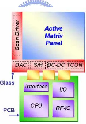
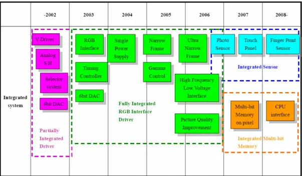
(11) Chapter 1 Introduction 1-1. Introduction to LTPS TFTs In recent years, the amorphous silicon thin film transistors (a-Si TFTs) are commonly used to be the switches of the pixel in active matrix liquid crystal displays (AMLCDs). Figure 1-1 shows the block diagram of active matrix display. All the driver chips are buried together with the other application-specified ICs on PCB because the current driving capacity of a-Si TFTs is not good enough for the system integration. However, the integration of driver circuitry with display panel on the same substrate is very desired not only because the need to reduce the module cost but to improve the system reliability. For this reason, the polycrystalline silicon thin-film transistors (poly-Si TFTs) have attracted much attention because of their wide applications in AMLCDs and organic light-emitting diodes (OLEDs) due to its high electron mobility. In polysilicon film, the carrier mobility larger than 100 cm2/Vs can be easily achieved, which is about 100 times larger than that of the conventional amorphous-silicon TFTs (with below 1 cm2/Vs). This characteristic allows the pixel-switching elements made by smaller TFTs size, resulting in higher aperture ratio and lower parasitic gate-line capacitance for the improvement of display performance. Furthermore, the integration of peripheral circuits in display electronics can be achieved by poly-Si TFTs due to its higher current driving capability, which is illustrated in figure 1-2. In addition to flat panel displays, poly-Si TFTs have also been applied into some memory devices such as dynamic random access memories (DRAMs), static random access memories (SRAMs), high programming read only memories (EPROM), and electrical erasable programming read only memories (EEPROMs) and three-dimensional(3D) ICs. Among the poly-Si technologies, low temperature polycrystalline silicon (LTPS) TFTs are primarily applied on glass substrates for the display electronics since the low process temperature could prevent the substrate from bending and twisting. LTPS TFT LCD technology has the feature of system integration within a display system. It can make a compact, highly reliable, display panel with high resolution. Because of this property, LTPS TFT LCD technology is widely used for mobile displays. Figure 1-3 shows the system integration roadmap of LTPS TFT LCD. Various integrated circuits, such as. 1.
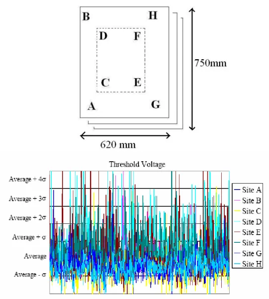
(12) vertical driver, horizontal driver including digital-to-analog converter (DAC), timing controller, power supply circuit (dc-dc converter), common driver, gamma circuit, have been developed so far [1]. Since 2004, a 6-bit RGB digital interface driver and power circuits completely integrated LCD has been successfully developed and commercialized for mobile phone handsets. More advanced driver integration for achieving a narrow edge frame and low voltage operation are now continuously being developed [1]. However, there are still some issues in LTPS TFTs such as reliability, device variation, and the speed limitation of device. On the other hand, there are some disadvantages in the SPICE simulation of TFTs model, such as the incapability of C-V model’s frequency dependence, the accuracy of TFTs DC and AC model, etc. However, in order to achieve the accurate behaviors for device performances, the understanding and implantation of these behaviors are desired. Therefore this thesis focuses on the behavior of device’s C-V characteristics with the view point into of the implantation in SPICE.. 1-2. Device variation The LTPS TFTs are found to suffer from serious variation of their electrical parameters [2-4]. The poly-Si material is a heterogeneous material made of small crystals of silicon atoms in contact with each other, constituting a solid phase material. These small crystals are called crystallites or grains. The irregular boundaries of these crystallites are the border lines of the grains. Because the material remains solid, the atoms at the border of a crystallite are also linked to the neighbor crystallite ones. However, these atom bonds are disoriented in comparison with a perfect lattice of silicon. This border is called a grain boundary. As the result of various distributions of grain boundaries in the channel of TFTs, the initial characteristics of LTPS TFTs are different from one another, which are shown in Figure 1.4. The Figure 1.5 shows site variation of the threshold voltage variation for an LTPS TFT fabrication line plotted in the format of lot trend and the degree of variation can be up to four times. of. the. standard. deviation.. These. variations. can. be. also. observed. in. Metal-Oxide-Semiconductor Field Effect Transistors (MOSFETs) but effects are more complicated in LTPS TFTs due to the random existence of grain boundaries. The device variation will lead to the variation of the circuit performance. It will be reflected directly on the image uniformity of the display. Besides, the effect of grain boundary may also influence the reliability behaviors of the devices affect stress. In addition to the circuit design in display, for the analysis of device behavior the device. 2.
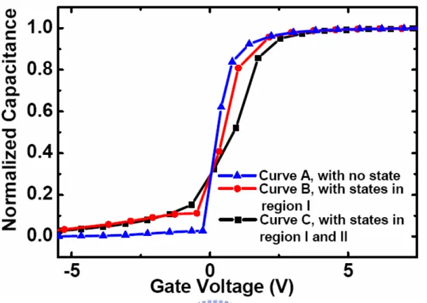
(13) variation must be taken into consideration. To avoid the confusion arisen from the device variation in our analysis, this thesis will use crosstie devices. The crosstie devices are equally spaced with a 40μm pitch arranged in a row. On the other hand, the crosstie devices are so close that the long range variation can therefore be ignored. Because between the different device has some is different, therefore all uses the identical device in mine research, compares the degradation around difference.. 1-3. Review of previous work In LTPS TFTs, several degradation mechanisms have been reported [5-13]. In 2002 Satoshi Inoue paper brought up the stress voltage dependence of the Vth shift in poly-Si TFTs, as shown in figure 1-6 [14]. Thus, in 2003 Satoshi Inoue’s paper classified the degenerated phenomena [15]. Figure 1-7 shows the effect of stress voltage on the Ion variation in TFTs. This result indicates two main degradation regions, the stress voltage of region A and region B. At first, hot carrier degradation is considered to originate from the damage of the metal-oxide-semiconductor (MOS) interface and of the channel poly-Si layer near the drain of TFTs. On the other hand, self-heating degradation is thought to originate in breaking of Si-H bonds and regeneration of dangling bonds in the MOS interface and channel poly-Si layers. In region A, the dominant degradation mechanism is self-heating, both the drain and gate voltages are high, typically over 10V. In region B, the dominant degradation mechanism is hot carrier, only the stress drain voltage is high, typically over 10V, and gate voltage is low, typically from 2V to 5V. In this thesis, we discuss the capacitance-voltage (C-V) characteristics in the two main degradation regions.. 1-4. Motivation Figure 1-8 shows C-V curves of the device affect hot carrier stress. It is obvious that curves show apparent frequency dependency. Figure 1-9(a) and (b) respectively show the state condition in the band and physical diagram location in the TCAD simulation. The three state conditions are arranged such that the distance of the bottom of the conduction band EC and the center of the state distributions are 0.2 eV, 0.3 eV, 0.4 eV. Figure 1-9(c) is the simulated C-V curves of stressed device with the three state conditions. It can be seen that the capacitance would apparently stretch for the gate voltage is just above VFB for the trap condition C. TCAD simulation can explain hot carrier mechanism correct. However, TCAD. 3.
(14) simulation is not able to deal with frequency dependent effect. Figure 1-10 shows the CGS curves of the device after significantly stretches out and shifts in the positive direction after stress. Figure 1-11(a) shows the model of the cross section of the device after self heating stress. With increasing the density of states (DOS) locally around region Ⅰ and region Ⅱ in simulation. Figure 1-11(b) shows the simulation result with increased DOS. Again, TCAD simulation results can explain the increase and shift for the curves after self-heating stress [16]. Nevertheless it can not explain frequency dependence. Since the frequency dependence is important in the simulation of circuit and characterization of the devices, it would be necessary to find the appropriate C-V model, which is the goal of this study.. 1-5. Thesis Outline Chapter 1. Introduction 1-1. Introduction to LTPS TFTs 1-2. Device variation 1-3. Review of previous work 1-4. Motivation 1-5. Thesis outline. Chapter 2. Experimental 2-1. Device fabrication 2-1-1. N-type TFT device fabrication 2-1-2. P-type TFT device fabrication 2-2. Device measurement method 2-2-1. Parameter extraction method 2-3. Stress conditions Chapter 3. Frequency dependence 3-1. N-type initial curve 3-1-1. N-type initial C-V and I-V curve 3-1-2. Comparison between RDS and C-V curves of n-type 3-2. P-type initial curve 3-2-1. P-type initial C-V and I-Vcurve. 4.
(15) 3-2-2. Comparison between RDS and C-V curves of n-type 3-3. Discussion. Chapter 4. DC stress effects 4-1. Hot carrier 4-1-1. N-type I-V and C-V curve 4-1-2. Compare with n-type RDS and C-V curve 4-1-3. P-type I-V and C-V curve 4-1-4. Compare with p-type RDS and C-V curve 4-1-5. Discussion 4-2. Self-heating 4-2-1. N-type I-V and C-V curve 4-2-2. Compare with n-type RDS and C-V curve 4-2-3. P-type I-V and C-V curve 4-2-4. Compare with p-type RDS and C-V curve 4-2-5. Discussion 4-3. Circuit model Chapter 5. Conclusion References Figures and Tables. 5.
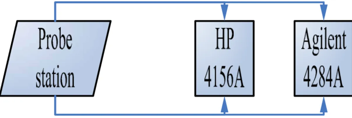
(16) Chapter 2 Experiments 2-1. Device fabrication In this study, the n-type TFTs with a channel width of 20μm and a channel length of 5 μm as well as the LDD structure of length 1.2μm are fabricated. The process flow of TFTs is described below. Firstly, the buffer oxide with a 50 nm thick a-Si:H films were deposited on glass substrates with plasma-enhanced chemical vapor deposition (PECVD), and then put the samples into the oven for dehydrogenation. The XeCl excimer laser of wavelength 308 nm with the energy density of 400 mJ/cm2 was applied. The laser scanned the a-Si:H film with the beam width of 4 mm and overlapped by 98% to recrystallize the a-Si:H film to poly-Si. After the poly-Si active area defined 80 nm SiO2 and 40 SiNx films were deposited with PECVD as the gate insulator. Next, the metal gate was formed by sputter and then was defined. The lightly doped drain (LDD) and the n+ source/drain doping were formed by PH3 implantation with dosage 2 x 10¹³ and 2 x 1015 cm2 of PH3, respectively. For the n-type devices, the LDD implantation was self-aligned and the n+ regions were defined with a separated mask. In addition, the p-type TFTs with a channel width of 20μm and a channel length of 5μ m are also fabricated. The process flow of p-type TFTs is very similar to the n-type ones. The only differences are the p+ source/drain doping was done by B2H6 self-align implantation with a dosage of 2 x 1015 cm-2, and the absence of LDD structure [17].. 2-2. Device measurement The electrical performance was measured with the Agilent 4156A semiconductor analyzer and Agilent 4284A precision LCR meter as shown in figure 2-3. The Agilent 4156A semiconductor analyzer with a probe station is used to analyze the electrical properties of a circuit such as I-V measurement or bias-temperature-stress (BTS). The ground probe station is furnished with an electrically isolated, water-cooled thermal plate within an optical shielding box. The source measurement units (SMUs) are used to control voltage sources where current flowing through can be measured. The voltage or current sources supplied by HP 4156A semiconductor analyzer can be transmitted through SMU to the device circuit and 6.
(17) the output voltage or current will be detected concomitantly. The C-V curves of the gate-to-source capacitance (CGS) and gate-to-drain capacitance (CGD) before and after stress with different frequencies are measured with the Agilent 4284A precision LCR meter. The CGS is measured between gate-and-source with floating drain. Similarly, the CGD measures the gate-to-drain one with floating source.. 2-2-1. Parameter extraction method The field effect mobility (µFE, Mu) is derived from the transconductance gm. The transfer characteristics of poly-si TFTs are similar to those of conventional MOSFETs, so is the first order I-V relation in the bulk Si. The MOSFETs can be applied to the poly-si TFTs, which can be expressed as. I D = µ FE Cox. W 1 [(VG − Vth )VD − VD 2 ] 2 L. (2-1). Where Cox is the gate capacitance per unit area, W is channel width, L is channel length,. Vth is the threshold voltage. If the drain voltage VD is much smaller compared with VG − Vth (i.e.VD << VG - Vth), then the drain current can be approximated as:. I D = µ FE Cox. W (VG − VTH )VD L. (2-2). And the transconductance is defined as:. gm =. ∂I D ∂VG. VD = const .. =. WC ox µ FE VD L. Therefore, the field effect mobility can be expressed as:. µ FE =. L gm C oxW V D. (2-3). We can get the field-effect mobility by taking the maximum value of the gm into (2-3) when VD = 0.1V In most of the researches on TFT, the constant current method is widely-adopted. In this thesis the threshold voltage is determined by this method, which extract Vth from the gate voltage at the normalized drain current Id=10nA for Vd=0.1V. The sub-threshold swing S.S (V/dec) is a typical parameter to describe the gate control. 7.
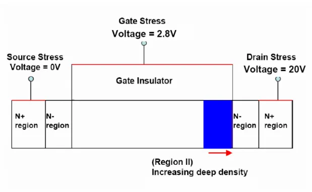
(18) toward channel. It is defined as the amount of gate voltage required to increase/decrease drain current by one order of magnitude. For the LTPS TFTs, the sub-threshold swing might increase with drain voltage due to short-channel effects. It might as well be affected by the serial resistance and interface traps and therefore become related to the gate voltage. In our thesis, it is defined as the minimum of the gate voltage required to increase drain current by one order of magnitude for VD = 0.1V.. ⎡ ∂ ( log I ds ) ⎤ S.S = ⎢ ⎥ ⎣⎢ ∂Vgs ⎦⎥. -1. (2-4). 2-3. Stress conditions As measured in the chapter 1, there are two main degeneration phenomena. We firstly conducted the stress of the hot carrier effect condition. For the n-type TFT, the gate bias (VGS) was set to the threshold voltage (about 1.8 V) of the TFT plus 1 V, while the drain bias (VDS) was 20 V [9]. For the p-type TFT, the VGS was set to the threshold voltage (about -2V) of the TFT minus 1 V and the VDS was -20V. One the other hand, for the self-heating effect condition, of the n-type TFT, the VGS was 18 V, while the VDS was 18 V. For the p-type TFT, the VGS was -18 V and the VDS was -18V. For all conditions, the TFTs were stressed 500 seconds. The stress conditions are listed in table 2-1.. 8.
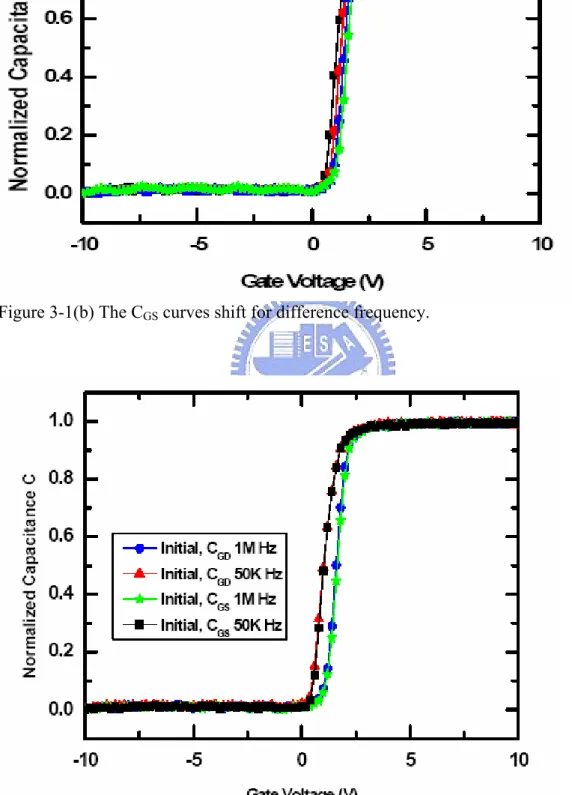
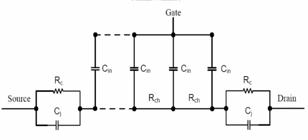
(19) Chapter 3 Frequency dependence 3-1. Initial characteristics of the n-type TFT In this chapter, we discuss the relation between C-V and I-V behaviors, and compare I-V and C-V curves with frequency dependence. Figure 3-1 (a) and (b) shows shift in the transient region of difference frequency. This shift could possibly result from the presence of states inside the poly-Si film. These states shift the threshold voltage for the onset of inversion by several tenths of mV for difference frequencies. These shifts owing to the intrinsic states may not be described detailed in the circuit model.. 3-1-1. Iitial C-V and I-V curves of the n-type TFT Figure 3-2 shows the initial C-V characteristics of n-type TFTs. The horizontal axis is the typical gate voltage and the vertical axis is the normalized capacitance. Here the gate voltage swept from -10V to 10V. We used two frequencies 50K Hz and 1M Hz to measure CGS and CGD curves. Figure 3-3 shows the initial I-V characteristics of the typical TFTs in the linear and saturate regions. The horizontal axis is the sweep gate voltage and the vertical axis is the drain current. Here the sweep gate voltage was varied from -10V to 15V, and the step drain voltages are 0.1V and 5V. It can be seen that in linearity and saturation the Vth is almost the same. And the threshold voltage of the I-V curve locates near the VFB of the C-V curve. On the other hand, I-V curve is in off region that C-V curve is at its minimum value. If I-V curve is in the on region, C-V curve will be at its maximum value. In order to explain the frequency dependence of the capacitance behaviors after stress, a circuit model consists of channel resistances and gate insulator capacitances is proposed, as shown in figure 3-4. For the unstressed device, the model is composed of the distributing insulator capacitance (Cin), channel resistance (Rch), junction capacitance (Cj), and contact resistance (RC). The C-V behavior and the I-V behavior can be correlated by considering the impedance of the device in this model. As the gate voltage is much higher than the Vth, the channel is turned on and the channel resistance will become very small in this case. The total impedance would be dominated by the insulator capacitance. Hence the major part of the signal current to be measured will flow through the channel resistance and the measured capacitance would be the summation of Cin. On the other hand, as the gate voltage is far. 9.
(20) below the Vth, the channel resistances Rch is high t such hat they would block the signal deep in the channel. Therefore, the measured C-V behavior in this region may actually represent the capacitance behaviors by the edges of the channel. However, for the transient region, neither the resistance nor the capacitance would dominate the impedance. Hence both the capacitance effect and the resistance effect should be considered. Since the capacitive impedance is frequency dependent, the frequency dependence of the measured C-V curves shown in figure 3-2 can be observed. It was found from the result that the I-V curves in linear off region was corresponding the C-V curve in minimum region. The results are shown in figure 3-5 (a). The RDS is greater when the Rch is open. On the other hand, the I-V curve in the on region was corresponding C-V curve in maximum region. The results are shown in figure 3-5 (b). The RDS is smaller when the Rch is short.. 3-1-2. Comparison between RDS and C-V curves of the n-type TFTs Figure 3-6 (a) and (b) shows the normalized CGS, CGD curves and the total resistances RDS at different C-V measuring frequencies, where the RDS is extracted from the ID-VG curves at VD=0.1 V. For the gate voltage is around Vth, the channel resistance would go through a transient region that the magnitude of the channel resistance would rapidly decrease from around 109 to 104 Ω. A critical point of the impedance behavior can be selected as the channel resistance Rch equals to the capacitance term 1/2πfCin, which just falls in the transient region of the CGS and CGD curves for the measuring frequency 50 KHz to 1 MHz. The term f represents the measuring frequency. The solid arrow in figure 3-6 represents the point that the total channel resistance RDS equals to the capacitance term 1/2πf CTFT for different C-V measuring frequency, where CTFT is 40 fF representing the gate insulator capacitance of the TFT. The upper dashed arrow represents the point PA where the channel resistance RDS is 10 times larger than the capacitance term 1/2πf CTFT, and the lower dashed arrow represents the point PB when the channel resistance RCH is 10 times smaller. In figure 3-5, the arrows respectively point out the 80 MΩ and 4 MΩ of the RDS, corresponding to the impedance of CTFT at the applied frequencies of 1M Hz and 50K Hz. The 80 MΩ and 4 MΩ two points are called PC. For the gate voltage lower than PA, the conductivity of the device is considered to be low enough that the channel resistance can be taken as open circuit and is labeled as the “open circuit region.” For the gate voltage larger than PB, the channel becomes so conductive to be considered as short circuit, and is labeled as “short circuit region”. Meanwhile, for the gate voltage between PA and PB, since the capacitive term and the resistive term of the. 10.
(21) impedance are comparable, neither of them can be ignored.. 3-2. Initial characteristics of the p-type TFT As pointed out in the previous section of n-type LTPS TFTs, its I-V and C-V can correspond to each of with the simplified circuit. Here we will discuss p-type the device behaviors.. 3-2-1. Initial I-V and C-V curve of the p-type TFT Figure 3-7 shows the initial C-V characteristics of typical TFTs. The horizontal axis is the sweep gate voltage and the vertical axis is the normalized capacitance. Here the sweep gate voltage was varied from -10V to 10V. We used two frequency 50K Hz and 1M Hz to measure CGS and CGD curves. Figure 3-8 shows the initial I-V characteristics of the linear and saturate regions in for the fresh TFTs. The horizontal axis is the sweep gate voltage and the vertical axis is the drain current. Here the sweep gate voltage was varied from -15V to 10V, and the step drain voltage was varied -0.1V and -5V. It can be seen that the in linearity and saturation the Vth is almost the same. It can be seen that threshold voltage of the I-V curve locates near the VFB the C-V curve. On the other hand, I-V curve is in the off region that C-V curve is in minimum value. If I-V curve is in the turn on region, C-V curve will be in maximum value. In order to explain the frequency dependence of the capacitance behaviors after stress, a circuit model of the channel resistances and the gate insulator capacitances is proposed, as shown in figure 3-4. For the unstressed device, the model is composed of the distributing insulator capacitance (Cin), channel resistance (Rch), junction capacitance (Cj), and contact resistance (RC). Although the p-type structure does not has LDD. The LDD affect Rch in the slicing model. The C-V behavior and the I-V behavior can be correlated by considering the impedance of the device in this model. As the gate voltage is much higher than Vth, the channel resistance will become very small and then the total impedance would be dominated by the insulator capacitance. Hence the major part of the signal current to be measured will flow through the channel resistance and the measured capacitance would be the summation of Cin. On the other hand, as the gate voltage is far below Vth, the channel resistances Rch are such high that they would block the signal deep in the channel. Therefore, the measured C-V behavior in this region may actually represent the capacitance behaviors beside the edges of the channel. However, for the transient region, neither the resistance nor the capacitance. 11.
(22) would dominate the impedance. Hence both the capacitance effect and the resistance effect should be considered. Since the capacitive impedance is frequency dependent, the frequency dependence of the measured C-V curves shown in figure 3-7 can thus be observed. It was found from the result that the I-V curve in linear off region was corresponding the C-V curve in minimum region. The results are shown in figure 3-5 (a). The RDS is greater when the Rch is open. On the other hand, the I-V curve in turn on region was corresponding C-V curve in maximum region. The results are shown in figure 3-5 (b). The RDS is smaller when the Rch is short.. 3-2-2. Comparison between RDS and C-V curves of the p-type TFTs Figure 3-9 (a) and (b) show the normalized CGS curves, CGD curves and the total resistance RDS at different C-V measuring frequency, where RDS is extracted from the ID-VG curves at VD=0.1 V. For the gate voltage is around VTH, the channel resistance would go through a transient region that the magnitude of the channel resistance would rapidly decrease from around 109 to 104 Ω. A critical point of the impedance behavior can be selected as the channel resistance Rch equals to the capacitance term 1/2πfCin, which just falls in the transient region of the CGS and CGD curves for the measuring frequency 50 KHz to 1 MHz. The term f represents the measuring frequency. The solid arrow in figure 3-8 represents the point that the total channel resistance RDS equals to the capacitance term 1/2πf CTFT for different C-V measuring frequency, where CTFT is 40 fF representing the gate insulator capacitance of the TFT. The upper dashed arrow represents the point PA where the channel resistance RDS is 10 times larger than the capacitance term 1/2πf CTFT, and the lower dashed arrow represents the point PB when the channel resistance Rch is 10 times smaller. In figure 3-8, the arrows respectively point out the 80 MΩ and 4 MΩ of the RDS, corresponding to the impedance of CTFT at the applied frequencies of 1M Hz and 50K Hz. The 80 MΩ and 4 MΩ two points are called PC. For the gate voltage lower than PA, the conductivity of the device is considered to be low enough that the channel resistance can be taken as open circuit and is labeled as the “open circuit region.” For the gate voltage larger than PB, the channel becomes so conductive to be considered as short circuit, and is labeled as “short circuit region”. Meanwhile, for the gate voltage between PA and PB, since the capacitive term and the resistive term of the impedance are comparable, neither of them can be ignored.. 12.
(23) 3-3. Discussion It is possible to establish two hypotheses. Firstly, if︱VG︱ smaller than︱PC︱, the measures capacitance is a minimum value. On the other hand,︱VG︱ greater than︱PC︱, the measures capacitance is the gate capacitance. It is considerable the validity in this theory. Thus this theory can be somehow explains frequency dependence.. 13.
(24) Chapter 4 DC stress effect 4-1. Hot carrier Hot carrier degradation is considered to originate from the damage of the MOS interface and channel active region near the drain of the device. The chapter will expand the idea into the field of LTPS TFTs. Hot carrier effect [5], as many works have reported, is closely related to the distribution of the lateral electric field in the channel and therefore is in relation with the applied drain voltage VDS and gate voltage VGS . Unlike in MOSFETs, hot carrier effect in TFTs becomes most severe as VGS is just above Vth and VDS is large [15]. Since the active region in the poly-Si TFTs contains many grain boundaries, the effect of hot carrier stress may be more complicated than that in MOSFETs.. 4-1-1. C-V and I-V curve of the n-type TFT Figure 4-1 (a) shows the normalized CGS curves before and after stress with different frequencies, and figure 4-1 (b) shows those of the CGD curves. The CGS is measured with a floating drain and CGD is measured with a floating source. The normalized capacitance is the ratio of the measured capacitance to a constant of 40 fF, which is the gate insulator capacitance of the TFT. The CGS curves of the stressed device show almost no difference as compared with the unstressed device. Nevertheless, the CGD curves of the device after stress show peculiar behaviors. The CGD curve of the stressed device measured at 50K Hz is almost the same as that before stress, but the curve at 1M Hz shows apparent stretch for the gate voltage is just above the flat band voltage VFB than the unstressed one. In other words, the degradation behavior of the CGD curves of the device after hot carrier stress is frequency dependent. In order to examine the frequency dependence of the C-V behavior of the devices after hot carrier stress, the CGS and CGD curves of the stressed devices at different applied frequencies are measured. Figure 4-2 (a) and (b) show the CGS and CGD curves of the device after hot carrier stress at measuring frequencies of 50 K, 100 K, 500 K and 1M Hz. The CGS curves of the stressed device show only slight shift for different applied frequency. However, in addition to the shift, the CGD curves show apparent stretch between different measuring frequencies for the gate voltage higher than VFB. The higher the measuring frequency applies, the more the CGD curve stretches. In order to understand the detailed degradation mechanism, I-V measurement is. 14.
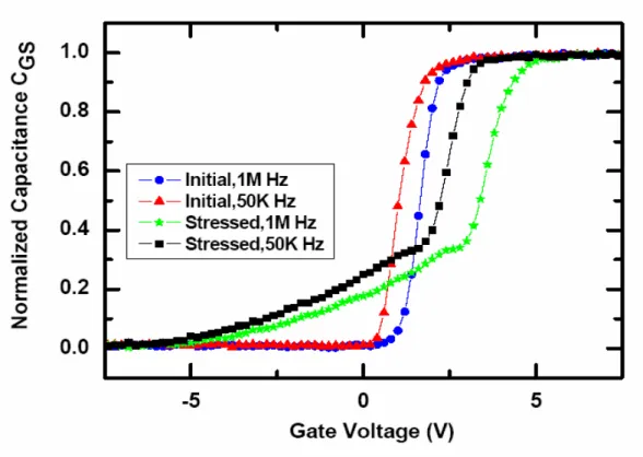
(25) employed. Figure 4-3 shows the ID-VG transfer characteristics before and after 500 seconds of hot carrier stress with the conventional forward and reverse connections. It can be seen that compared with the unstressed device, the stressed device shows lower on current and almost unchanged subthreshold region. However, the difference of the on current of the stressed device between the forward and reverse connection indicates that the states distribute in the more the drain. On the other hand, I-V curve is in off region that C-V curve is in minimum. If I-V curve is in turn on region, C-V curve will is in maximum.. 4-1-2. Comparison between RDS and C-V curves of the n-type TFT Figure 4-4 (a) and (b) are the normalized capacitance characteristics of CGS and CGD with the total resistance RDS extracted from the ID-VG curves for the device after hot carrier stress. However, the PC is the reference point in RDS curve and in C-V curve. For the gate voltage lower than PA, the conductivity of the device is considered to be low enough that the channel resistance can be taken as open circuit and is labeled as the “open circuit region.” For the gate voltage larger than PB, the channel becomes so conductive to be considered as short circuit, and is labeled as “short circuit region”. For the gate voltages near the critical point, the capacitive term and the resistive term of impedance to be measured are comparable; both the effect of the Cdeg and channel conductance would take place. Since the capacitive impedance is frequency dependent, the C-V curves should be analyzed considering the measuring frequency. For the low measuring frequency of 50 KHz, the capacitive term 1/2πf CTFT is relatively larger than the channel resistance at the gate voltage slightly larger than Vth. Therefore the measured CGS and CGD characteristics would quickly contain the gate capacitance in the channel and saturate at CTFT. Therefore the effect of the degradation component Cdeg may not be obvious. However, for the high measuring frequency of 1MHz, the channel resistance can be ignored till the gate voltage is much larger than Vth and thus the effect of the Cdeg components can be apparent. In other words, the degradation in the C-V behaviors for the LTPS TFTs may only be observed at higher measuring frequencies, where the effect of the degraded capacitances is not covered.. 4-1-3. C-V and I-V curve of the p-type TFT Figure 4-5 (a) shows the normalized CGS curves before and after stress with different frequencies, for the p-type devices and figure 4-5 (b) shows those of the CGD curves. After stress, the CGD curve at difference frequencies will both increase in the off region. The increase in the CGD could be explained that the operation increases the overlapped capacitance.. 15.
(26) On the other hand, after stress the CGS value was not altered, and hence the phenomenon may due to the charge trapping near the drain. Figure 4-6 shows the I-V curves before and after stress. The I-V curves do not show obvious difference. The leakage current was decreased in the forward measurement. The phenomenon indicates that the electric filed in the channel edge near the drain was decreased [5]. This phenomenon is similar to the hot-electron-induced punchthrough (HEIP) [18-20]. The primary hot-carrier degradation mechanism of PMOSFETs has been attributed to negative charge trapping in the gate oxide. The injection of electrons into the oxide causes drain extension and thus reduces the effective channel length. This mechanism is called HEIP. This mechanism would result in the increase of the transconductance with stress time and therefore the on current would increase. For the carriers comes from the localized and nonuniform buildup of interface traps and oxide traps near the drain junction. The mechanism could well the p-type TFTs phenomenon.. 4-1-4. Comparison between RDS and C-V curves of the p-type TFT Figure 4-7 (a) and (b) are the normalized capacitance characteristics of CGS and CGD with the total resistance RDS extracted from the ID-VG curves for the device after hot carrier stress. The PC is the reference point in RDS curve and in C-V curve. For the gate voltage lower than PA, the conductivity of the device is considered to be low enough that the channel resistance can be taken as open circuit and is labeled as the “open circuit region.” For the gate voltage larger than PB, the channel becomes so conductive to be considered as short circuit, and is labeled as “short circuit region”. The result observes the same as each other. The RDS curve explains frequency dependence that is correct.. 4-1-5. Discussion In the n-type TFTs, because the hot carrier stress induces extra trap states near the drain, the CGD curve shows degradation in high frequency. Therefore in the circuit model, the model has a parallel Cdeg near the drain produced during stress. On the other hand, the model has the Rch change near the drain. In the p-type TFTs, the degradation was attributed to electron trapping in the gate insulator near the drain. So the circuit model has the Rch change slightly near the drain. In this case, for the stressed device, the CGD curves show higher capacitance for the gate voltage smaller than VFB, where the device is presumed to be OFF and no capacitance show be measured.. 16.
(27) 4-2. Self-heating Self-heating degradation is thought to originate in breaking of Si-H bonds and regeneration of dangling bonds in the MOS interface and channel poly-Si layers [14-15]. It was confirmed that if the temperature of TFTs during operation reached over 300℃ due to self-heating. The TFTs will were degraded, and the temperature was the main factor responsible for this degradation.. 4-2-1. C-V and I-V curve of the n-type TFT Figure 4-8 (a) shows the CGS curves before and after stress with different frequencies, while figure 4-8 (b) shows the corresponding curves of CGD. Compared to the curves before stress, the stressed CGS and CGD curves exhibit two main changes, namely, the positive shift for the gate voltage near the flat band voltage VFB and the increase for the gate voltage just below VFB. The stretch and shift in the positive direction for the gate voltage near VFB are considered to be attributed to the increase of the deep states during stress. On the other hand, the increases of the C-V curves for the lower gate voltage possibly come from the interface states. Figure 4-9 shows the I-V transfer characteristics for the TFT before and after stress. The stress condition is that both VGS and VDS equal to 18V. For the stressed devices, it can be seen that the Vth and the subthreshold swing increase, and the on current decreases. On the other hand, I-V curve is in off region that C-V curve is in minimum. If I-V curve is in turn on region, C-V curve will is in maximum.. 4-2-2. Comparison between RDS and C-V curves of the n-type TFT Figure 4-10 (a) and (b) are the normalized capacitance CGS and CGD and the total resistances RDS extracted from the ID-VG curves. However, the PC is the reference point in RDS curve and in C-V curve. For the gate voltage lower than PA, the conductivity of the device is considered to be low enough that the channel resistance can be taken as open circuit and is labeled as the “open circuit region.” For the gate voltage larger than PB, the channel becomes so conductive to be considered as short circuit, and is labeled as “short circuit region”. In the open circuit region, since all the channel resistances are taken as opened, the model is reduced to only the capacitances in the device. Thus the Cdeg resulting from the interface states and the Cdeep from the self-heating effect would lead to the increase of the CGS and CGD curves for the lower gate voltage, respectively. In this region, the different frequency dependences for CGS and CGD reflect the different responses of the states near the source and the drain, respectively.. 17.
(28) As the gate voltage increases, two effects make the CGS and CGD curves change with gate voltage. The proposed model may fairly explain the frequency-dependent degradation of the capacitance curves after both the hot carrier and self-heating stress conditions.. 4-2-3. C-V and I-V curve of the p-type TFT Figure 4-11 (a) shows the CGS curves before and after stress for the p-type device affect self-heating stress with different frequencies, while figure 4-11 (b) shows that curves of CGD. Compared with the curve before stress, the CGS curves and the CGD curves of the stressed device exhibit two main changes, namely, the negative shift for the gate voltage near the flat band voltage VFB and the increase for the gate voltage just below VFB. Figure 4-12 shows the I-V transfer characteristics for the TFT before and after stress. The stress condition is that both VGS and VDS equal to -18V. For the stressed device, it can be seen that the Vth from negative direction [21]. On the other hand, I-V curve is in off region that C-V curve is in minimum. If I-V curve is in turn on region, C-V curve will is in maximum.. 4-2-4. Comparison between RDS and C-V curves of the p-type TFT Figure 4-13 (a) and (b) are the normalized capacitance CGS and CGD and the total resistance RDS extracted from the ID-VG curves. However, the PC is the reference point in RDS curve and in C-V curve. For the gate voltage lower than PA, the conductivity of the device is considered to be low enough that the channel resistance can be taken as open circuit and is labeled as the “open circuit region.” For the gate voltage larger than PB, the channel becomes so conductive to be considered as short circuit, and is labeled as “short circuit region”. However, we explain the open circuit region and short circuit region still establishment. For the reasons mentioned above, it can be concluded that the hypothesis was supported.. 4-2-5. Discussion In n-type TFTs, the C-V curve increases in off region. Therefore in the circuit model, the model has a Cdeep near the drain produced during stress and the model has a Cdeg production near the source. On the other hand, the model has the Rch change near the drain. In p-type TFTs, the C-V curve shift negative direction the same as I-V curve phenomenon. Therefore, the circuit model has the Rch changed hugely in the channel.. 18.
(29) 4-3. Circuit model Figure 4-14 shows the circuit model after stress. The circuit model has a Cdeg near the drain and source. After stress the Rch may be changed near the drain. In p-type TFTs, the circuit model only change the Rch'near the drain after stress. In n-type TFTs, for hot carrier stress the circuit model has a parallel Cdeg production and the Rch change the Rch'near the drain. For the self-heating stress in the n-type TFTs, the circuit model has a parallel Cdeg production near the drain and source and the Rch change the Rch' in the channel.. 19.
(30) Chapter 5 Conclusion and future work 5-1. Conclusion In this thesis, the degradation of LTPS TFTs under hot carrier and self heating stress was investigated using C-V method. For the hot carrier stress, it is found that the degradation of the CGD curves would exhibit apparent frequency dependence for different measuring frequencies in n-type device. On the other hand, the p-type exhibits the HEIP mechanism. For the self-heating stress, it is found that high gate voltage that the phenomena explain by the temperature rise owing to Joule-induced heating. A circuit model connecting the I-V and C-V behaviors is proposed to explain the anomalous C-V behavior. Via this model, the C-V behaviors can be divided into three regions by comparing the resistive term and the capacitive term of the total impedance. It is proposed that the frequency dependence of the CGD curves after hot carrier stress reflects the transient behaviors of the channel resistances and capacitances. In addition, it is discovered that the self heating stress would cause the increase of deep states in the poly-Si film near the drain, and the interface states at the interface in the source region. The RDS curve and the circuit model explain the frequency dependence in the I-V behaviors. It was found from the result that frequency dependence and circuit model can explain the C-V curves the initial devices, the C-V curves for the hot carrier, and self-heating conditions. This finding would provide important information for the further studies of the C-V behaviors, frequency dependence and its relation to the I-V behaviors of LTPS TFTs.. 5-2. Future work The quasi-static C-V measures would be applied to further verify our model. In future, it is desired that the correct C-V circuit model to put in SPICE simulation model. We hope that the precise C-V simulation model can help panel designers in estimating and evaluating the SOP panel design. The newly established thin film transistor electric circuit model can put in the middle of the simulation software to help designers with faster and convenient understanding device’s characteristics and design conditions. Hence, the designers can compute a more complex electric circuit within shorter design period to achieve the target of having an advanced breakthrough in designing system on panel (SOP) circuit. On the other. 20.
(31) hand, the technology development can help the display panel show the vivid images than the present product.. 21.
(32) Figure 1-1. The block diagram of an active matrix display. Figure 1-2. The integration of peripheral circuits in a display achieved by poly-Si TFTs. 22.
(33) Figure 1-3. The roadmap from 2002 to 2008 Ref. Y.Nakajima et al.,SID’ 06. Figure 1-4. The initial characteristics of LTPS TFTs are different from one another due to various distributions of grain boundaries. 23.
(34) Figure 1-5. The site variation of the threshold voltage variation for LTPS TFT fabrication line plotted in the format of lot trend. 24.
(35) Figure 1-6. Stress voltage dependence of the VT shift of the TFTs. Ref. Satoshi Inoue et al.JJAP’03. Figure 1-7. Dependence of stress voltage on the Ion variation in the TFTs. Ref. Satoshi Inoue et al.JJAP’02. 25.
(36) Figure 1-8. The measurement hot carrier C-V curve before and after. .. Figure 1-9(a) With increasing the density of states (DOS) locally around region Ⅱ.. 26.
(37) Figure 1-9(b) The model of the cross section n-type device after hot carrier stress.. Figure 1-9(c) The simulation result of C-V curve before and after.. 27.
(38) Figure 1-10. The measurement self heating C-V curves before and after stress.. Figure 1-11(a) The model of the cross section device after self heating stress. Ref. Y.H.Tai ECS’06. 28.
(39) Figure 1-11(b) The simulation result of C-V curve before and after DOS. Ref. Y.H.Tai et al.ECS’06. Table 2-1. Stress conditions.. 29.
(40) Figure 2-1. The n-type devices cross sectional.. Figure 2-2. The p-type devices cross sectional. 30.
(41) Figure 2-3. The device measurement equipment measure picture.. Figure 3-1(a) The CGD curves shift for difference frequency.. 31.
(42) Figure 3-1(b) The CGS curves shift for difference frequency.. Figure 3-2. The initial n-type measures C-V curves.. 32.
(43) Figure 3-3. The initial n-type measures I-V curves.. Figure 3-4. The n-type slices circuits.. 33.
(44) Figure 3-5(a) The slices circuit that the Rch is open.. Figure 3-5(b) The slices circuit that the Rch is short.. 34.
(45) Figure 3-6(a) The n-type CGS with RDS curves.. Figure 3-6(b) The n-type CGD with RDS curves.. 35.
(46) Figure 3-7. The initial p-type measures C-V curve.. Figure 3-8. The initial p-type measures I-V curve.. 36.
(47) Figure 3-9(a) The p-type CGS with RDS curves.. Figure 3-9(b) The p-type CGD with RDS curves.. 37.
(48) Figure 4-1(a) Normalized CGS curves (before and after hot carrier stress) versus gate voltage at frequencies 50K and 1M Hz.. Figure 4-1(b) Normalized CGD curves (before and after hot carrier stress) versus gate voltage at frequencies 50K and 1M Hz.. 38.
(49) Figure 4-2(a) Normalized CGS curves for the device after hot carrier stress at different frequencies 50K, 100K, 500K and 1M Hz.. Figure 4-2(b) Normalized CGD curves for the device after hot carrier stress at different frequencies 50K, 100K, 500K and 1M Hz.. 39.
(50) Figure 4-3. Current transfer characteristics before and after hot carrier stress conditions with the forward and reverse connections.. Figure 4-4(a) The normalized CGS curves and the RDS curves for the device after hot carrier stress.. 40.
(51) Figure 4-4(b) The normalized CGD curves and the RDS curves for the device after hot carrier stress.. Figure 4-5(a) Normalized CGS curves (before and after hot carrier stress) versus gate voltage at frequencies 50K and 1M Hz.. 41.
(52) Figure 4-5(b) Normalized CGD curves (before and after hot carrier stress) versus gate voltage at frequencies 50K and 1M Hz.. Figure 4-6. Current transfer characteristics before and after hot carrier stress conditions with the forward and reverse connections.. 42.
(53) Figure 4-7(a). The normalized CGS curves and the RDS curves for the device after hot carrier stress.. Figure 4-7(b) The normalized CGD and the RDS curves for the device after hot carrier stress.. 43.
(54) Figure 4-8(a) Normalized CGS curves (before and after self-heating stress) versus gate voltage at frequencies 50K and 1M Hz.. Figure 4-8(b) Normalized CGD curves (before and after self-heating stress) versus gate voltage at frequencies 50K and 1M Hz.. 44.
(55) Figure 4-9. Current transfer characteristics before and after self-heating stress condition with the forward and reverse connections.. Figure 4-10(a) The normalized CGS curves and the RDS curves for the device after self heating stress.. 45.
(56) Figure 4-10(b) The normalized CGD curves and the RDS curves for the device after self heating stress.. Figure 4-11(a) Normalized CGS curves (before and after self-heating stress) versus gate voltage at frequencies 50K and 1M Hz.. 46.
(57) Figure 4-11(b) Normalized CGD curves (before and after self-heating stress) versus gate voltage at frequencies 50K and 1M Hz.. Figure 4-12. Current transfer characteristics before and after elf-heating stress condition with the forward and reverse conditions.. 47.
(58) Figure 4-13(a) The normalized CGS curves and the RDS curves for the device after self heating stress.. Figure 4-13(b) The normalized CGD curves and the RDS curves for the device after self heating stress.. 48.
(59) Figure 4-14. The circuit model is after stress.. 49.
(60) References [1] Y. Nakajima, et al., “Ultra-Low-Power LTPS TFT-LCD Technology Using a Multi-Bit Pixel Memory Circuit”, SID 06 Digest, pp.1185-1188, 2006. [2] Kitahara, Yoshiyuki, Toriyama, Shuichi, Sano, Nobuyuki, “A new grain boundary model for drift-diffusion device simulations in polycrystalline silicon thin-film transistors”, Japanese Journal of Applied Physics, Part 2: Letters, v 42, n 6 B, pp. L634-L636, 2003. [3] Wang, Albert W. and Saraswat, Krishna C., “Modeling of grain size variation effects in polycrystalline thin film transistors”, Technical Digest – International Electron Devices Meeting, pp. 277-280, 1998. [4] Wang, Albert W. and Saraswat, Krishna C., “Strategy for modeling of variations due to grain size in polycrystalline thin-film transistors”, IEEE Transactions on Electron Devices, v 47, n 5, pp. 1035-104, 2000. [5] Kook Chul Moon, Jae-Hoon Lee, and Min-Koo Han, “The study of hot-carrier stress on poly-Si TFT employing C-V measurement”, IEEE Transactions on Electron Devices, v 52, n 4, April, pp. 512-517, 2005. [6] K.C. Moon, et al., “Observation of electron trapping in p-type polycrystalline silicon thin film transistors due to hot carrier stress employing C-V measurement,” AM-LCD ‘03, TFTp3-6. [7] D.K. Schroder, “Semiconductor material and device characterization”, 2nd Edition, John Wiley & Son, pp.337-404, p543-546, 1998. [8] A. Schwerin, W. Hansch, and W. Weber, “The relation between oxide charge and the device degradation : A comparison study of n- and p- channel MOSFETs,“ IEEE Trans. Electron Devices, vol. 34, no. 12, pp. 2493-2500, Dec. 1987 [9] K.M. Han and C.T. Sah, “Positive oxide charge from hot hole injection during channel hot electron stress,” IEEE Trans. Electron Devices, vol. 45, no. 7, p. 1624, Jul. 1998 [10] Y. Byun, M. Shur, M. Hack, and K. Lee, "New Analytical Poly-Silicon Thin-Film Transistor Model for CAD and Parameter Characterization," Solid State Electronics, vol. 35, No. 5, pp. 655-663, 1992. [11] A. A. Owusu, M. D. Jacunski, M. S. Shur, and T. Ytterdal, "SPICE Model for the Kink Effect in Polysilicon TFTs," 1996 Electrochemical Society Fall Meeting, San Antonio, TX, Oct., 1996. [12] B. Faughan, “Subthreshold Model of a Polycrystalline Silicon Thin-Film Field-Effect Transistor,” Appl. Phys. Lett., vol. 50, no. 5, pp. 290-292, 1987. [13] Shur, M. Hack, and Y. H. Byun, "Circuit Model and Parameter Extraction Technique for Polysilicon Thin Film Transistors", in Proc. of the 1993 Int’l. Semiconductor Device Research Symp., ISDRS'93, Charlottesville, VA, pp. 165-168, 1993. [14] S. Inoue, H. Ohshima, T. Shimoda, “Analysis of Degradation Phenomenon Caused by. 50.
(61) [15]. [16]. [17]. [18]. [19]. [20]. [21]. Self-Heating in Low-Temperature-Processed Polycrystalline Silicon Thin Film Transistors”, Japanese Journal of Applied Physics , Part 1, v41, pp. 6313-6319, 2002 S. Inoue, H. Ohshima, T. Shimoda, “Fabricated by a Low-Temperature Process Using Emission Light Microscopy Analysis of Degradation Phenomenon Caused by Self-Heating in Low-Temperature-Processed Polycrystalline Silicon Thin Film Transistors”, Japanese Journal of Applied Physics , Part 1, v42, pp. 1168-1172, 2003 Y.H. Tai, S.C. Huang, H.L. Chiu, “Degradation of capacitance-voltage characteristics induced by self-heating effect in poly-Si TFTs”, Electrochemical and Solid-State Letters, v 9, n 6, June, pp. G208-G210, 2006 S.C. Huang, Y.H. Kao, Y.H Tai, “Study on electrical degradation of p-type low-temperature polycrystalline silicon thin film transistors with C-V measurement analysis”, Thin Solid Films, v 515, n 3, Nov 23, pp. 1206-1209, 2006 K. Cheng, et al., “Separation of hot-carrier-induced interface trap creation and oxide charge trapping in PMOSFETs studied by hydrogen/deuterium isotope effect”, IEEE Electron Device Letters, v 22, n 4, April, pp. 188-190, 2001 Ouisse Thierry, Cristoloveanu Sorin, Borel Gerard, “Hot-carrier-induced degradation of the back interface in short-channel silicon-on-insulator MOSFETs”, IEEE Electron Device Letters, v 12, n 6, Jun, pp. 290-292, 1991. S. Mahapatra, et al., “Direct charge pumping technique for spatial profiling of hot-carrier induced interface and oxide traps in MOSFETs”, Solid-State Electronics, v 43, n 5, May, pp. 915-922, 1999. Yasuyoshi Mishima, et al., “Characteristics of low-temperature poly-Si TFTs on Al/glass substrates”, IEEE Transactions on Electron Devices, v 48, n 6, June, pp. 1087-1091, 2001. 51.
(62) Vita. 52.
(63)
數據

+7
相關文件
Wang, Solving pseudomonotone variational inequalities and pseudocon- vex optimization problems using the projection neural network, IEEE Transactions on Neural Networks 17
Then, a visualization is proposed to explain how the convergent behaviors are influenced by two descent directions in merit function approach.. Based on the geometric properties
volume suppressed mass: (TeV) 2 /M P ∼ 10 −4 eV → mm range can be experimentally tested for any number of extra dimensions - Light U(1) gauge bosons: no derivative couplings. =>
Define instead the imaginary.. potential, magnetic field, lattice…) Dirac-BdG Hamiltonian:. with small, and matrix
incapable to extract any quantities from QCD, nor to tackle the most interesting physics, namely, the spontaneously chiral symmetry breaking and the color confinement..
• Formation of massive primordial stars as origin of objects in the early universe. • Supernova explosions might be visible to the most
雙極性接面電晶體(bipolar junction transistor, BJT) 場效電晶體(field effect transistor, FET).
(Another example of close harmony is the four-bar unaccompanied vocal introduction to “Paperback Writer”, a somewhat later Beatles song.) Overall, Lennon’s and McCartney’s
