Voltage Scaling and Temperature Effects on Drain Leakage Current
Degradation in a Hot Carrier Stressed n-MOSFET
Tahui Wang, C.F. Hsu, L.P. Chiang. N.K. Zous. T.S. Chao* and C.Y. Chang Department of Electronics Engineering, National Chiao-Tung University
*National Nan0 Devices Lab.,
fax:886-3-5724361 ;email: wang@ jekyll.ee.nctu.edu.tw Hsin-Chu, Taiwan, R.O.C.
ASSTRACT
Drain leakage current degradation at zero V in a hot carrier stressed n-MOSFELT is measured and modeled. h e dependences of drain leakage current on supply voltage and temperature are characterized. In modeling, various drain leakage current mechanisms including drain-to-source subthreshold leakage current, band-to-band tunneling current and interface trap assisted leakage ciment are taken into account. Our result shows that interface trap induced leakage current appears to be a dominant drain 1,:akage mechanism as the supply voltage is scaled below 3.0V. Drain leakage current degradation by orders of magnitude has been observed due to hot carrier stress.
blTRODUCnON
The reduction of drain leakage current at zero Vgs has been a major concem in CMOS device scaling. Gate induced drain leakage (GIDL) current resulting from band-to-band tunneling has been recognized as one of the major drain leakage mechanisms in thin-oxide MOSFETs [l]. Recently, hot carrier stress effects on device degradation have received much interest [2-61. However, most of the studies concentrate on stress induced on-state drain current reduction [2,3]. The stress effect on off-state drain leakage current degradation has not received as much attention [4,7]. The stress effect on drain leakage current is attribuud to the creation of oxide trapped charge and interface traps. The build-up of negative oxide charge shifts the device flat-band voltage and results in an enhancement of band- to-band tunneling current. In addition, the generated interface traps can introduce an additional trap-assisted leakage mechanism [8]. At scaled supply voltages, while band-to-band tunneling can be greatly alleviated, the trap-assisted current may appear to be a dominant leakage mechanism. Furthermore, experimental results showed that the trap-induced leakage current exhibits a dependence on temperature [9]. In a certain bias range, the lcakage current becomes much aggravated as temperature rises and thus may have impact on a DRAM refresh time. In this woik, it is our intention to investigate the hot carrier stress effect on drain leakage current degradation in thin- oxide MOSFETs. The drain leakage current mechanisms at different supply vlaltages and temperatures are characterized and modeled.
DRAIN
LEAKAGE CURRENT MECHANISMSVarious drain leakage paths in a stressed MOSFET are considered in our model. The trap-independent leakage mechanisms include band-to-band tunneling current
(Im)
and drain-to-source subthreshold current (IS),IBB = M?exp(-B/Et) ( 1 )
Is
=roexp(-ev,,)
(2)nkT
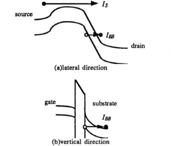
where the parameters A and B are d e f i e d in Ref. [lo]. Et denotes the total Si surface field. Drain junction leakage current is small in this work and can be neglected. Fig. 1 illustrates these two components in the lateral direction and in the vertical direction respectively.
+
Is
drainL
(a)lateral directiongate^^
substrate (b)vertical directionFig. 1 Illustration of subthreshold leakage current
(Is)
and band- to-band tunneling current(lm)
(a) in the lateral direction and (b) in the vertical direction.The interface trap assisted leakage mechanisms are the Shockley-Read-Hall current ( ~ J s R H ) . thermionic-field emission current
(a&.
and sequential tunneling current (&TAT). A complete trap-assisted drain-to-substrate leakage path at the Si/SiO2 surface is formed by hole emission from traps to the valence band and electron emission from traps to the conduction band. Both electron emission and hole emission are carried out via either thermionic emission or field emission. The carrier transition processes are drawn in Fig. 2. In the figure, Ge and Ghstand for electron and hole thermionic emission rates and Te and
Th denote electron and hole tunneling rates. Each carrier transition rate is formulated as follows,
(9
where on and
up
are electron and hole capture cross sections, &i and stand for the intrinsic Fermi-level and trap energy. fv ,fr
and f , are the electron occupation factors in the valence band, trap states and in the conduction band, respectively. ns and ps are electron and hole concentrations at the Si surface, which are calculated from a two-dimensional device simulation.
re
and 2 hare electron and hole tunneling times from the WKB approximation. In a steady-state, the trap occupation factor
ft
can be evaluated from the equalityGe+Te=Gh+Th
with fc=O and fv= 1. The three trap-assisted leakage current components are therefore expressed in the following [8],where dL is the width of the interface trap ( W i t ) region and
W
is the channel width. The total trap-assisted leakage current d l d is the summation of the above three components,(a) lateral direction
(b)
vertical direction
lateral direction and (b) in the vertical direction. Note that
TA
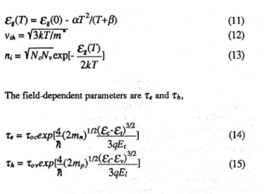
only occurs in the lateral direction.The temperature-dependent parameters used in the calculation are bandgap (&g), thermal velocity (vth) and intrinsic concentration (ni ). They are given below [ 113,
The fielddependent parameters are Ze and Zh,
where
roc
and rOv are effective transit times in the conduction band and in the valence band, is the surface field in the lateral direction and other variables have their usual definitions. Note that the hole tunnelingTh
occurs only in the lateral direction. Thus,Th
is a function of only a lateral field whereas the tunnelingprocess 1~ and
Te
are dependent on a total field.DEVICE
CHARACTEREATTON
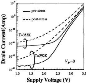
The test device is a 0.35p.m n- T with source/drain extension. The gate oxide thicknes ut 40A and the gate width is 100pm. The device was subject to maximum substrate current stress Vg8=2V and Vh=4.5V for 3000 seconds. The pre- stress and post-stress Id -Vgs characteristics are shown in Fig. 3 (T=292K) and in Fig. 4 (T=353K), respectively. Under the stress condition, interface trap generation is almost saturated and oxide charge creation is minimal [7]. Interface trap generation is
evidenced by the change of the subthreshold swing in Figs. 3 and 4. The
DIBL
effect is not significant in the device.-1.0 -0.5 0.0 0.5 1.0 1.5
Gate-to-source
Bias,
Vgs
(V)
10.' n
E
2-
10.'E"
z
n
w
c)8
10-l1 10." .I ed tcr -1.0 -0.5 0.0 0.5 1.0 1.5Gate-to-source Bias, Vgs
(V)
Fig. 4 Measured Ire-stress and post-stress Id -Vss characteristics at V,=1.5\' and 3.0V, T=353K.
RESULTS
AND
DISCUSSIONS
The dependence of pre-stress and post-stress drain leakage currents on supply voltage (VdJ is measured in Fig. 5. The leakage current enhancement factor, defined as the ratio of the post-stress drain leakage to the pre-stress drain leakage at T=292K, is shown in Fig. 6. The trap effect on the leakage current enhancement becomes particularly pronounced around a supply voltage of 2.2V. An enlargement of the drain leakage current by a factor of 18 is obstmed at T=292K. Various drain leakage current components lM, 158 and the trap induced d l d are plotted in Fig. 7. The solid lines are the measured result and the circles represent the calculated result.
-
pre-stress-pI
/' 0 1 1.0 1.5 2 0 2.5 3.0 3.5Supply Voltage (V)
Fig. 5 Measured ckain leakage current characteristics before and after stresf. at two different temperatures, T=292K and T=353K.
120
T=353K
1.3 1.7 2.1 2.5 2.9 3.3
Supply Voltage (V)
Fig. 6 The ratio of the post-stress drain leakage current to the pre-stress (T=292K) drain leakage current versus supply voltage.
The interface trap density
Nit
used in the calculation is 1 . 4 ~ 1 0 ~ ~ c m - ~ and the length of the trap distribution (AL) is 400A.a,,
and 0, in Eqs. (3) and (4) are 1015cm2[11]. The following features are observed. At a large supply voltage (Vd3.OV). the band-to-band tunneling current (I@) manifests itself as a dominant mechanism even in a stressed device. In addition. the trap induced component d l d exhibits a weaker field dependence than the 1~ due to a smaller tunneling barrier from traps to the conduction band (electron tunneling) or to the valence band (hole tunneling). As a result, as the supply voltage scales, theIm
drops more quickly and the A I d appears to be a major drain leakage mechanism in a stressed device. When the V u is further reduced, the tunneling effect becomes unimportant. The enhancement of the drain leakage is achieved mainly through theSRH
component. Therefore, the enhancement factor in Fig. 6 peaks around 2.2V. At T=353K, the enhancement factor in Fig. 6is significantly increased up to 110. The temperature effect is apparent at a lower V u The enhancement factor at V&=1.3V increases from about 5 at T=292K to 80 at T=353K. The [M, fs
and the A I d at T=353K are shown in Fig. 8.
10"
10-13
1.3 1.7 2.1 2 5 2.9 3.3
Supply Voltage (V)
Fig. 7 Various drain leakage current components at T=292K from measurement (solid lines) and calculation (full circles).
10-8
T=353K
-
measurement 10-8T=353K
E .111E
1 6 "n
Is 1.3 1.7 2.1 2.5 2.9 3.3Supply Voltage (V)
Fig. 8 Various drain leakage current components at T=353K from measurement (solid lines) and calculation (full circles).
d l d reprensents the trap-induced drain leakage.
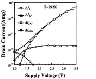
Furthermore, the components in the a d are analyzed in Fig. 9 (T=292K) and in Fig. 10 (T=353K). In Fig. 9, the trap- induced drain leakage is dictated by the &AT for vdd >1.7v, by the
d l ~ ~
for 1.7v?V&.5v, and by the NSRH for 1.SVrVdd In Fig. 10, the thermally related components AZTF and NSRH are more prominent. As the supply voltage scales, the field dependent cunent component (A~TAT) can be greatly alleviated, while the temperature dependent components ( ~ T F and AZSRH)become dominant drain leakage mechanisms.
1.3 1.7 2.1 2.5 2.9 3.3
Supply Voltage (V)
Fig. 9 Calculation of various interface trap induced drain leakage current components at T=292K.
The vertical field and the lateral field effects on drain leakage current are also assessed. Our calculation reveals that the band-to- band tunneling, current is mainly contributed by the vertical field whereas the trap-assisted tunneling is mostly determined by the lateral field due to the dependence of T h (hole tunneling) only on the lateral field.
1.3 1.7 2.1 2.5 2.9 3.3
Supply Voltage (V)
Fig. 10 Calculation of various interface trap induced drain leakage current components at T=353K.
CONCLUSIONS
The band-to-band tunneling current is found to be a dominant drain leakage mechanism at V e 3 . 3 V in the current device structure. At a reduced supply voltage, the trap-induced current appears to be the major leakage component. We have observed that hot carrier stress can degrade the drain leakage current by orders of magnitude. While the vertical field has a larger effect on the band-to-band tunneling current, the trap- induced leakage is mostly caused by lateral field enhanced tunneling. The reduction of lateral field is necessary to suppress the trap-induced drain leakage in deep submicron devices.
ACKNOWLEDGEMENT
Financial support from National Science Council,
ROC,
is gratefully acknowledged. The authors also would like to express thanks to Dr. Chimoon Hung at Macronix Inc. for many fruitful discussions.REFERENCES
J. Chen. T.Y. Chan, P.K. KO, and C. Hu, 'Subbreakdown Drain Leakage Current in MOSFET,' IEEE Electron Device Lett. Vol. EDL-8, pp. 515-517. 1987.
T. Tsuchiya, "Trapped-electron and Generated Interface Traps in Hot Electron Induced MOSFET Degradation," IEEE Trans. Elect. Dev.
,
Vol. ED-34, pp. 2291-2296,1987.
T. Wang, C. Huang, P. C. Chou,
S. S.
Chung and T. E. Chang, "Effects of Hot Carrier Induced Interface State Generation in Submicron LDD MOSFET's. " IEEE Trans.Efect. Dev. , Vol. ED-41, pp. 1618-1622, 1994. H. Sasaki, M. Saitoh, and K. Hashimoto, "Hot-carrier Induced Drain Leakage Current in n-channel MQSFET,"in IEDM Tech. Dig., pp. 726-729, 1987.
C. Duvvury, D. I. Redwine, and H. J. Stiegler, "Leakage Current Degradation in N-MOSFETs due to Hot-electron Stress,'' IEEE Electron Device Lett., Vol. EDL-9, pp.579-58 1, 1988.
G. Q.
Lo,
A. B. Joshi, and D-L, Kwong, "Hot-carrier- stress Effects on Gate-induced Drain Leakage Current in nchannel MOSFET's," IEEE Electron Device Lett., Vol. A. Frommer, M.R.
Pinto, and J. D. Bude, "Two-Stage Leakage Degradation in Sub-Micron MOSFET Technology", Symp. on VLSI Tech., pp.164-165, 1996[8] T. Wang, T. E. Chang, and Chimoon Hung, "Interface Trap Induced Thermionic and Field Emission Current in Off-State MOSI'ETs" in IEDM Tech. Dig., pp.161-164,
1994.
[9] C. T. Wang, Hot Carrier Design Consideration for MOS Devices and Circuits, Van Nostran Reinheld, 1992 [lo] T. Y. Chan, J. (:hen, P. K.
KO,
and C. Hu. 'The Impactof Gate-induced Drain Leakage Current on MOSFET Scaling," in IEllM Tech. Dig., pp. 721-724, 1987. [ll]