國
立
交
通
大
學
資訊科學與工程研究所
碩
士
論
文
非同步雙道超大指令字組處理器之資料路徑設計
Data Path Design for Asynchronous two-way VLIW Processor
研 究 生:李國成
指導教授:陳昌居 教授
非同步雙道超大指令字組處理器之資料路徑設計
Data Path Design for Asynchronous two-way VLIW Processor
研 究 生:李國成 Student:Guo-Cheng Li
指導教授:陳昌居 Advisor:Chang-Jiu Chen
國 立 交 通 大 學
資 訊 科 學 與 工 程 研 究 所
碩 士 論 文
A ThesisSubmitted to Institute of Computer Science and Engineering College of Computer Science
National Chiao Tung University in partial Fulfillment of the Requirements
for the Degree of Master
in
Computer Science September 2010
Hsinchu, Taiwan, Republic of China
i
非同步雙道超大指令字組處理器之資料路徑設計
研究生:李國成
指導教授:陳昌居 教授
國立交通大學資訊科學與工程研究所
摘 要
過去數十年來,計算機架構發展快速,然而因為過去技術上的困難,在1940年代開 始計算機架構的設計方式為了避免很多在非同步電路系統中可能衍生的問題而選擇了 有clock的設計方式,因此現今大部分處理器都以同步系統為基礎而持續發展中。 然而這幾年來,處理器的發展已經由高時脈進入平行處理發展階段。到目前為止處 理器的設計方向轉向多核心處理器發展,試圖以多核心處理器的技術來取代高時脈以達 到效能提升的目的,而時脈造成的耗電與熱能皆無法有效避免。而處理器在非同步系統 的發展也有持續研究與成果展現,如:由英國曼徹斯特大學(University of Manchester) 發表的AMULET系列微處理器。因此本篇論文嘗試以非同步系統為基礎實作出一個架構簡 單、適合建構成多核心處理器的超長指令字組非同步核心,期望未來把多個輕量化非同 步核心以interconnection network作連結變成一個多核心非同步處理器。最後我們將 這個超長指令字組非同步核心以Synopsys Design Compiler來做合成,使用的是TSMC 0.13微米的元件資料庫並且以ModelSim 6.0模擬及驗證設計的正確性。ii
Data Path Design for Asynchronous two-way
VLIW Processor
Student:
Advisor:Dr. Chang-Jiu Chen
Institute of Computer Science and Engineering College of Computer Science
National Chiao Tung University
Abstract
Most modern processors are based on synchronous circuit design nowadays. The current trend of processors is towards multiprocessor because the higher power consumption and heat energy caused by clock distribution. Moreover, embedded multimedia system and Digital Signal Processor are more and more popular in recent years. DSPs are developed for handling a large number of image data. They improve performance with VLIW and SIMD in some instances. However, they are all based on synchronous circuit design. The clock distribution may cause a serious problem in complex systems.
In this study, we try to design a light-weight core based on asynchronous circuit design. It is an asynchronous two-way VLIW processor and includes some special instructions for SIMD application. In the future, we can develop an asynchronous multi-core processor which is made up of this asynchronous two-way VLIW processor via interconnection network. Finally, the correct of function is verified by ModelSim 6.0 and synthesized by TSMC .13μ m process library.
iii
Acknowledgement
這篇論文的完成,首先要感謝我的指導教授陳昌居老師的細心指導,在老師的教學 風格下讓我有自由的發揮空間。其次要感謝實驗室的幾位博士班學長緯民、宏岳以及元 騰在做研究期間給予熱心指導、建議與校稿,讓本篇論文得以順利完成。也感謝實驗室 的同學與學弟,在研究期間給予的鼓勵,以及家人的支持,讓我能夠專心完成研究學業。iv
CONTENTS
摘 要 ... i Abstract ... ii Acknowledgement ... iii CONTENTS ... iv List of Figures ... viList of Tables ... vii
CHAPTER 1 INTRODUCTION ... 1
1.1MOTIVATIONS ... 1
1.2THE ORGANIZATION OF THIS THESIS... 2
CHAPTER 2 BACKGROUND AND RELATED WORKS ... 3
2.1ASYNCHRONOUS CIRCUIT DESIGN ... 3
2.1.1 Advantages ... 3 2.1.2 Handshaking Protocol ... 5 2.1.3 Muller C-element ... 9 2.1.4 Asynchronous Pipelines ... 10 2.2PROCESSORS OVERVIEW ... 13 2.2.1 AMULET Microprocessors ... 13
2.2.2 Microchip’s PIC18 and NCTUAC18 ... 14
2.2.3 TITAC ... 17
2.2.4 DSPs ... 18
CHAPTER 3 DESIGN AND IMPLEMENTATION ... 19
3.1ARCHITECTURE OVERVIEW... 19
3.2INSTRUCTION SET ... 22
3.3CONSTRUCT THE BASIC ELEMENTS ... 27
3.3.1 Registers ... 28
3.3.2 Dual-rail Gates ... 29
3.3.3 C-Latch ... 30
3.3.4 DeMUX and MERGE ... 30
v
3.3.6 MAC and LDST Function Units ... 33
3.4INSTRUCTION SET ... 35 3.4.1 Pipeline Architecture ... 36 3.4.2 ID Stage ... 37 3.4.2.1 Register Bank ... 39 3.4.3 EX Stage ... 42 3.4.3.1 EX1 Stage ... 44 3.4.3.2 EX2 Stage ... 45 3.4.3.3 WB Stage ... 45 CHAPTER 4 SIMULATION ... 47 4.1TESTING ENVIRONMENT ... 47 4.2AREA SIMULATION ... 48 4.3TIMIING SIMULATION ... 48
CHAPTER 5 CONCLUSIONS AND FUTURE WORKS ... 50
vi
List of Figures
Figure 2.1 (a) Bundled-data channel ... 6
Figure 2.1 (b) Four-phase handshaking protocol ... 6
Figure 2.2 (a) Dual-rail channel ... 7
Figure 2.2 (b) Four-phase dual-rail protocol ... 8
Figure 2.3 Transfer diagram ... 8
Figure 2.4 Two-phase handshaking protocol ... 9
Figure 2.5 (a) Muller C-element ... 10
Figure 2.5 (b) Muller C-element with reset signal ... 10
Figure 2.6 Muller pipeline ... 11
Figure 2.7 (a) Four-phase bundled-data pipeline ... 12
Figure 2.7 (b) Four-phase bundled-data pipeline with data processing and delay element ... 12
Figure 2.8 Four-phase dual-rail piepline architecture (2-bit wide) ... 12
Figure 2.9 Architecture of AMULET1... 13
Figure 2.10 System block of diagram of PIC18 ... 15
Figure 2.11 Block diagram of APIC18 with 4-stage pipeline architecture ... 16
Figure 2.12 The pipeline architecture of TITAC-2 ... 17
Figure 3.1 Architecture Overview ... 20
Figure 3.2 Register file ... 22
Figure 3.3 Pack instruction ... 27
Figure 3.4 (a) 1-bit Register ... 28
Figure 3.4 (b) Zero Register ... 29
Figure 3.5 The 2-bit dual-rail AND gate ... 29
vii
Figure 3.7 DeMUX and MERGE ... 31
Figure 3.8 Memory Interface ... 32
Figure 3.9 Block diagram of LDST function unit ... 33
Figure 3.10 Block diagram of MAC function unit ... 34
Figure 3.11 Pack unit ... 35
Figure 3.12 Unpack unit ... 35
Figure 3.13 Pipeline Architecture ... 36
Figure 3.14 Control Path ... 38
Figure 3.15 Block diagram of ID stage ... 38
Figure 3.16 Register bank ... 39
Figure 3.17 Block diagram of Lock Module ... 40
Figure 3.18 (a) Path A ... 43
Figure 3.18 (b) Path B ... 44
viii
List of Tables
Table 2.1 Encoding Method ... 7
Table 2.2 Function behaviors of Muller C-element ... 9
Table 2.3 Basic categories of instruction set of PIC18 and their operand needed ... 15
Table 3.1 Issue of instruction ... 21
Table 3.2 Instruction Formant ... 23
Table 3.3 Instruction Set ... 26
Table 3.4 The truth table of 2-input dual-rail AND gate ... 29
Table 4.1 The area report of each stage ... 48
Table 4.2 The area report of register bank... 48
1
CHAPTER 1 INTRODUCTION
1.1 MOTIVATIONS
Most microprocessor designs are based on synchronous circuit design in past decades. In order to improve the performance of processor, the technique of microprocessor design is made progress from pipeline to superscalar and VLIW in recent years. But they were based, for the most part, on higher frequency of clock such as Intel Pentium 4 [14]. The higher frequency of clock may cause more power consumption and heat energy. As frequency of clock is getting higher, the problem is getting worse. So the policy of microprocessor design is changed into multiprocessor such that attempting to reduce the influence of these problem caused by higher frequency of clock. There are some instances for this police, for example, IBM Cell Broadband Engine [13].
Furthermore, embedded multimedia system and Digital Signal Processor are more and more popular in recent years. Comparing with general purpose processor mentioned in above, DSPs are developed for handling a large number of image data. They used some techniques, such as VLIW and SIMD, to improve performance. However, they are all based on synchronous circuit design. When cores in processor become more and more large, the clock distribution may be a serious problem in complex systems.
In our implementation, we aim at designing an asynchronous two-way VLIW processor with asynchronous circuit design. It is implemented to avoid some problem such as clock
2
skew and worst-case timing delay in synchronous circuit design by the advantages of asynchronous circuit [1]. Moreover, we also design the datapath to support the functions of DSP, such as SIMD and MAC. The design policies of our two-way VLIW processor are simple and modular in order to build a light-weight core which is used to construct multiprocessor with asynchronous circuit design in the future.
1.2 THE ORGANIZATION OF THIS THESIS
This thesis proposes the datapath design of asynchronous two-way VLIW processor. In Chapter 1, the motivation is presented. In Chapter 2, some basic asynchronous circuit design concepts and related works which include some microprocessors for general purpose in asynchronous circuit design today will be introduced. In Chapter 3, we introduce datapath of our two-way VLIW processor, instruction set architecture, and pipeline architecture. In Chapter 4, we show the simulation result and area report. Finally, a conclusion and future works are shown in Chapter 5.
3
CHAPTER 2 BACKGROUND AND RELATED
WORKS
This section will introduce what is asynchronous circuit design, ex: advantages, handshaking protocols, Muller Pipeline, Muller C-element of asynchronous circuit design [1]. Two pipeline architectures of processor are also listed in this chapter.
2.1 ASYNCHRONOUS CIRCUIT DESIGN
Asynchronous circuits design is a kind of circuit design methodology. Asynchronous circuit is practically different from synchronous circuit because all components communicate with each other by handshaking protocols in asynchronous circuit, whereas share and notice the clock signal in synchronous circuit. The following will list subjects about asynchronous circuits design.
2.1.1 Advantages
Comparing with the synchronous circuit design, the asynchronous circuit design has no global clock. As a result of no global clock, the asynchronous circuit design has some benefits:
Low power consumption: Asynchronous circuits do not need to generate global clock to fire component, and therefore could save power caused by clock tree. Moreover, each module works only when and where needed, this means that module is idle at the other time.
4
No clock distribution and clock skew problems:In synchronous circuit, components communicate with each other by clock distribution. Clock skew is a serious problem. Asynchronous circuit is in opposition to synchronous circuit on this question because there is no clock in asynchronous circuit.
Average-case performance: The elasticity of asynchronous pipeline has led to the result that the asynchronous pipeline can work in average case time rather than worst case time for pipeline stage. When component in asynchronous circuit has been completed its job, it could sent a request signal to receiver and wait to perform next new job until receiver send acknowledge signal back. However, the pipeline of synchronous circuits select the longest time for the stage which need more time slice. On the contrary, asynchronous pipeline allow every stage work in individual time due to handshaking protocol. Hence, asynchronous pipeline could works in average-case performance.
Modularity: Different modules from different designers may have different clock distribution in synchronous circuit design. To combine two or more components will probably become a challenge. Due to handshaking interface and individual time for every stage, it can be done easily in asynchronous circuit design. Designers do not need to maintain synchronization between distinct modules. Each module has its complete time and does not influence other modules.
5
communicate with each other by handshaking protocols, area and power consumption due to the control logic for handshaking are unavoidable.
2.1.2 Handshaking Protocol
Handshaking protocol is used to communicate between two components in asynchronous circuit design. It can be separated some solution space as the cross product as following: { two-phase, four-phase} x { bundled-data, dual-rail, 1-of-n, …}.
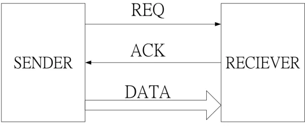
In this solution space of handshaking protocol, the bundled-data and dual-rail data are the two most common data encodings. The four-phase bundled-data protocol is usually used for asynchronous circuit designs (Figure 2.1). It has two control signals, REQ and ACK, between SENDER and RECEIVER used to control all of transfer steps (Figure 2.1 (a)). The four-phase handshaking protocol is also known as return-to-zero protocol because REQ and ACK signals have to return to zero when a transaction is completed between SENDER and RECEIVER (Figure 2.1 (b)). Initially, REQ and ACK signals are all “0”. When valid data arrive or ready at SENDER, REQ is set to “1” and sent to RECEIVER by SENDER (1). Then, RECEIVER has accepted the data from SENDER, ACK is set to “1” and sent to SENDER by RECEIVER (2). After SENDER receives the ACK signal from RECEIVE, REQ is set to “0” (3), and then RECEIVER will pulls down ACK signal to “0” when receives REQ = 0 from SENDER, too (4). After these four steps, SENDER and RECEIVER complete a handshaking. At this time, SENDER and RECEIVER can start next transaction (5).
6
SENDER
RECIEVER
REQ
DATA
ACK
Figure 2.1 (a) Bundled-data channel.
REQ
ACK
DATA
1
3
4
2
Figure 2.1 (b) Four-phase handshaking protocol.
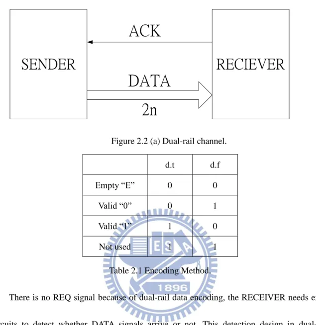
The other way of four-phase handshaking protocol is four-phase dual-rail data protocol (Figure 2.2 (a)). Compared with data channel of four-phase bundled-data protocol, it has no REQ signal. Dual-rail channel encodes 1-bit data with 2-bits. The encoding method is shown in Table 2.1. It use 00 to express there is no data in EMPTY state, 01 to encode the data of 0 and 10 to encode the data of 1 in VALID state, respectively. By the way, the 11 is not used in dual-rail data encoding. If the system uses dual-rail data encoding to transfer n-bits data, it has 2*n data lines to indicate a valid data.
7
SENDER
RECIEVER
DATA
ACK
2n
Figure 2.2 (a) Dual-rail channel. d.t d.f Empty “E” 0 0
Valid “0” 0 1 Valid “1” 1 0 Not used 1 1
Table 2.1 Encoding Method.
There is no REQ signal because of dual-rail data encoding, the RECEIVER needs extra circuits to detect whether DATA signals arrive or not. This detection design in dual-rail circuits is called complete detection.
Figure 2.2 (b) shows the process of data transfer using dual-rail protocol. Initially, DATA is EMPTY, and ACK signal is 0. When DATA is Valid and RECEIVER detects that DATA is ready, RECEIVER captures DATA and pulls up ACK. Then SENDER stops sending valid DATA and changes state of DATA to EMPTY. Finally, RECEIVER pulls down ACK signal to 0 and this transaction is completed.
8
ACK
DATA
EMPTY VALID EMPTY VALIDFigure 2.2 (b) Four-phase dual-rail protocol.
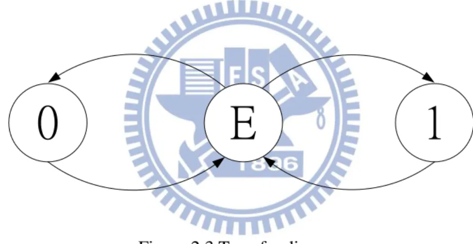
Valid DATA is separated by EMPTY token in four-phase dual-rail protocol. SENDER must return to EMPTY state after RECEIVER captures the valid DATA. Then, it can start next transaction. Thus, the sequence of state is EMPTY – VALID – EMPTY – VALID (Figure 2.3).
E
1
0
Figure 2.3 Transfer diagram
The two-phase handshaking protocol is different from all of above due to the meaning of the signal edges. As showing in Figure 2.4, a signal transition means that a transaction between SENDER and RECEIVER is completed. The rising edges and falling edges in two-phase handshaking protocol have no difference. For example, when the data of SENDER is ready, SENDER sets the REQ to “1” (initial:“0”). Then RECEIEVER gets data and sends ACK signal to SENDER with “1” (initial:“0”). This transaction is completed, and next transaction starts with REQ changed into “0” at SENDER side. Two-phase handshaking
9
protocol is also known as non-return-to-zero protocol.
REQ
ACK
DATA
Figure 2.4 Two-phase handshaking protocol.
2.1.3 Muller C-element
Muller C-element [1] is a basic component in asynchronous circuit design. It is used to state-holding or construct the latch between pipeline stages. The function behaviors of Muller C-element are shown in Table 2.2. When both inputs are 0, the output Z is set to 0. When both inputs are 1, the output Z is set to 1. If the inputs are different (ex:01、10), the output Z will keep previous output. In other words, the output Z is only changed when all inputs are the same. Figure 2.5 (a) shows the symbol and gate-level design of C-element, and Figure 2.5 (b) shows the C-element with reset signal.
Input A Input B Output Z
0 0 0
0 1 No change
1 0 No change
1 1 1
10
A
A
B
B
C
Z
Z
Figure 2.5 (a) Muller C-element.
A
A
B
B
C
Z
Z
reset
reset
Figure 2.5 (b) Muller C-element with reset signal.
2.1.4 Asynchronous Pipelines
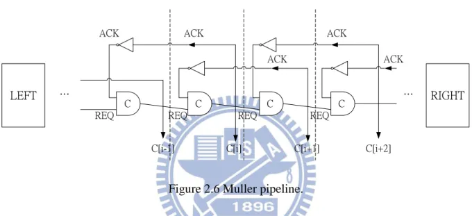
Muller pipeline is a pipeline architecture with four-phase bundled-data protocol [1]. Most of asynchronous pipeline is based on Muller pipeline (Figure 2.6). Muller pipeline has several characteristics as following:
11
1. It is delay-insensitive handshake machine.
2. When pipeline is full, only half of the latches of pipeline store data.
3. If the RIGHT side is slower than the LEFT side, this pipeline may fill and stall.
4. Timing depends on local delays, so Muller pipeline could work in average case performance.
LEFT RIGHT
REQ ACK
REQ REQ REQ
ACK
ACK
ACK
ACK
C[i-1] C[i] C[i+1] C[i+2]
C C C C
… …
Figure 2.6 Muller pipeline.
Figure 2.7 (a) shows the four-phase bundled data pipeline [1] which based on Muller pipeline. It is similar to synchronous pipelines and master-slave flip-flops. In order to maintain correct behaviors, matching delay should be inserted in the request signal paths. Figure 2.7 (b) shows a four-phase bundled data pipeline with data processing and delay element on REQ signal.
12
C
Latch Latch Latch
En En En
REQ REQ REQ
ACK
ACK
ACK ACK
REQ
C C
Figure 2.7 (a) Four-phase bundled-data pipeline
C
Latch Latch Latch
En En En
REQ REQ REQ
ACK
ACK
ACK
ACK
REQ
Latch Latch Latch
Delay Delay C Delay C
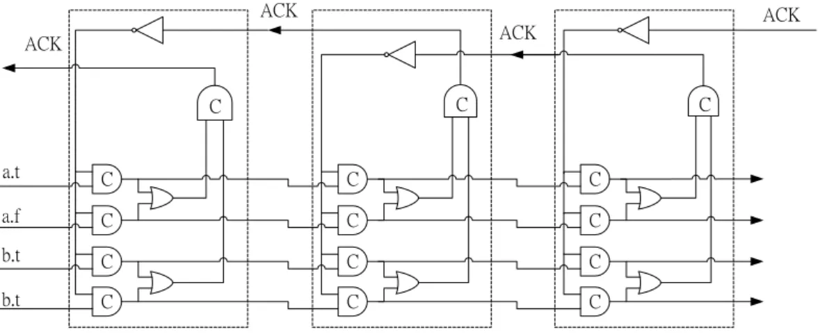
Figure 2.7 (b) Four-phase bundled-data pipeline with data processing and delay element. A four-phase dual-rail pipeline is also based on Muller pipeline with the request eliminated by the 1-of-2 data encoding. Figure 2.8 shows the four-phase dual-rail pipeline model [1], and it must have complete-detection mechanism composed of or-gate because there are not REQ lines.
C ACK ACK ACK ACK C C C C C C C C C C C C C C a.t a.f b.t b.t
13
2.2 PROCESSORS OVERVIEW
In this section, we will introduce some solution about processor with asynchronous circuit design; in addition, we’ll also describe some popular Digital Signal Processors (DSPs) today. They are AMULETs [2, 3, 4], Microchip’s PIC18, NCTUAC18 [5], and TITAC [7, 8], which are based on asynchronous circuit design. SPXK5 [9], TMS320C55x [10], and TMS320C64x [11] are based synchronous circuit design.
2.2.1 AMULET Microprocessors
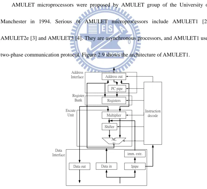
AMULET microprocessors were proposed by AMULET group of the University of Manchester in 1994. Serious of AMULET microprocessors include AMULET1 [2], AMULET2e [3] and AMULET3 [4]. They are asynchronous processors, and AMULET1 uses two-phase communication protocol. Figure 2.9 shows the architecture of AMULET1.
Address out PC pipe Registers Multiplier Shifter imm. extr. Ipipe Data in Data out Instruction decode AL U Address Interface Register Bank Data Interface Excute Unit
14
AMULET2e is a redesign of AMULET1 for embedded systems with on-chip memory. It is implemented with four-phase handshaking protocol. AMULET3 was also redesigned architecture and presented between 1996 and 1998. It has branch target prediction and goal of higher performance than AMULET1 and AMULET2e.
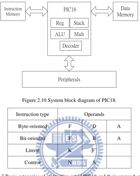
2.2.2 Microchip’s PIC18 and NCTUAC18
The PIC18 is developed by Microchip. Figure 2.10 shows the system block diagram and Table 2.3 lists the basic categories of instruction set of PIC18 and their operands needed. There are some characteristics of PIC18 as following:
1. It is an 8-bit RISC microcontroller based on the Harvard architecture.
2. There are two memories: instruction memory (up to 2MB) and data memory (up to 4MB) follow 16-bit wide instruction and 8-bit wide data respectively. PIC18 has 16 banks of 256 bytes data memory.
3. It provides 77 available instructions. 4. Two-stage instruction pipeline.
15 Reg Stack ALU Mult Decoder Instruction Memory Data Memory Peripherals PIC18
Figure 2.10 System block diagram of PIC18. Instruction type Operands
Byte-oriented F D A Bit-oriented F B A
Literal K F’
Control N S
Table 2.3 Basic categories of instruction set of PIC18 and their operands needed. The meaning of letter in Table 2.3 is list in the following:
F: The file register. It means which file register is to be used by the instruction.
D: The destination of the result. It specifies where the result of the operation is to be placed. A: The accessed memory.
B: The bit in the file register. It selects the number of the bit affected by the operation. K: A literal value to be loaded in a file register.
16
N: A program memory address.
S: The mode of the CALL or RETURN instructions.
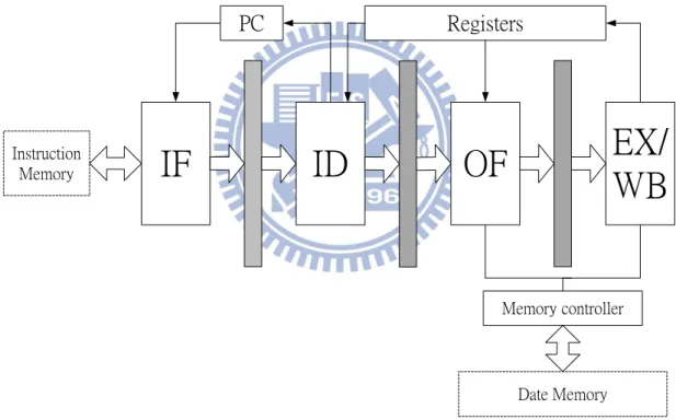
The NCTUAC18 was proposed by NCTU in 2009 [5]. It is also a RISC processor which implemented with asynchronous circuit design based on QDI delay-model and four-phase dual-rail handshake protocol. The execution and write back stage are combined to one stage to avoid data hazard. Figure 2.11 shows the block diagram of APIC18 with 4-stage pipeline architecture. Instruction Memory Date Memory
IF
ID
OF
EX/
WB
Memory controller PC RegistersFigure 2.11 Block diagram of APIC18 with 4-stage pipeline architecture.
A new implementation, APIC18S, to solve this performance degradation was proposed by NCTU in 2007 [6].
17
2.2.3 TITAC
TITAC and TITAC-2 [7, 8] developed in Tokyo Institute of Technology are asynchronous processor. They are implemented with two-phase dual-rail handshaking protocol. TITAC is a 8-bit asynchronous processor with a single-accumulator architecture based on quasi-delay-insensitive (QDI) delay model [1]. TITAC-2 [8] developed in 1997 is a 32-bit asynchronous processor. It is based on scalable-delay-insensitive (SDI) delay model [8]. There is a 8-Kbyte instruction cache on TITAC-2. In addition, the instruction set of TITAC-2 is similar to MIPS-R2000. The instructions are classified into ten categories as following: logical, arithmetic, multiply, divide, compare, shift, load, store, branch, and privileged instructions. Figure 2.12 shows the block diagram of TITAC-2 with 5-stage pipeline architecture.
IF
ID
EX
ME
Memory controller PC RegistersWB
I-cache address data Write buffer18
2.2.4 DSPs
Digital signal processor is particular microprocessor used for fast operation about digital signal processing. In general, it requires large number of mathematical operations for image or audio processing. Many digital signal processors exist today such as SPXK5 [9], TMS320C55X, and TMS320C64x developed by TEXAS INSTRUMENTS [10, 11]. Follows are some features of digital signal processors.
1. Based on Harvard architecture.
2. There are some special instructions for SIMD. 3. Memory architecture is designed for streaming data.
4. Multiply-accumulates unit (MACs) is used for highly arithmetic operations 5. Bit-reversed addressing for calculating FFTs.
6. In order to improve the whole performance, VLIW techniques could support digital signal processor in instruction level parallelism.
19
CHAPTER 3 DESIGN AND IMPLEMENTATION
We introduce the background of asynchronous circuit design and list some processors designed by asynchronous circuit in previous sections. In this chapter, we will describe pipeline architecture in details and focus on datapath of our two-way VLIW microprocessor. The result of simulation will present in Chapter 4.3.1 ARCHITECTURE OVERVIEW
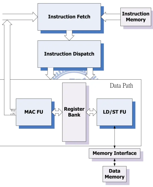
All of components of our two-way VLIW microprocessor are implemented based on 4-phase dual-rail handshaking protocol, QDI delay model, and developed with Verilog hardware description language. Figure 3.1 shows the architecture overview of our two-way VLIW microprocessor.
There are two memories: Instruction Memory (64-bit wide), Data Memory (32-bit wide). The datapath includes Register Bank, MAC function unit, LDST function unit, and a 40-bit accumulator in MAC function unit. The instruction packets are constructed of two 32 bits long instructions. If the two instructions cannot be executed in parallel, they are packed into different instruction packet. This job can be done in Instruction Fetch stage and Instruction Dispatch stage. After Instruction Dispatch stage, the two instructions of 64-bit instruction packet are issued to appropriate datapath. The first instruction is executed in MAC function unit, and the other is operated in LDST function unit.
20
Program Counter Module handles the execution sequence of instructions. It includes an increment unit to perform PC+1. The effective target address which is decided by branch instruction to jump is selected in Program Counter Module.
Register Bank Instruction Fetch Instruction Dispatch MAC FU LD/ST FU Instruction Memory Data Memory Writ e PC Memory Interface
Data Path
21
Instruction type MAC LDST Arithmetic operations ● ● Multiplication/Divison ● ● MAC (multiply-accumulates) ● Branch ● Load/Store ● SIMD ● ●
Table 3.1 Issue of instruction.
There are 32 registers in register file (Figure 3.2). Five are system registers among them, zero register ($0), stack pointer ($sp), repeat count ($rp), return address ($ra), and basic block ($bb). Twelve could support SIMD operation to be divided into two 16-bit register ($sd0H, $sd0L, …). Fifteen are general-purpose 32-bit registers. Table 3.1 lists what kinds of instructions are executed in MAC function unit or LDST function unit. Pipeline architecture, instruction set architecture, MAC FU, and LDSD FU will be described in details in following section.
22 $0 $sp $rp $ra $bb $g0 $g1 $g13 $g14 … $sd0H $sd0lL $sd1H $sd1L $sd10H $sd10L $sd11H $sd11L … Five system registers Twelve SD registers Fifteen general purpose registers
Figure 3.2 Register file
We use fixed-point number representation system in our design. The digit-vector is denoted by X = (X31, X30, …, X1, X0). The X can represent three kinds of numbers in our
number system. They are signed integers, unsigned integers, and unsigned real numbers. The signed integers can represent from -231-1 to 231-1. The unsigned integers can represent from 0 to 232-1. The unsigned real numbers are denoted by fixed<16, 16>. The first half of bit pattern (X31, X30, …, X17, X16) means non-negative numbers, and the last half of bit pattern means
fraction. For example, if X = 00000000000101111000000000000000, it is 23.5 (0000000000010111.1000000000000000) in fixed-point number representation system.
3.2 INSTRUCTION SET
Our instruction set architecture is similar to MIPS. Each instruction is 32 bits long that divided into several fields. The instructions can be classified into two categories as following: R-type operations
23
Table 3.2 shows the instruction format and Table 3.3 lists our available instructions.
5 bits 5 bits 5 bits 5 bits 5 bits 6 bits 1 bit R-type/MAC Opcode Rd Rs Rt Shamt Funt P bit I-type Opcode Rd Rs Immediate P bit
Table 3.2 Instruction Format
The meaning of each fields of instruction format is described in the following: Opcode: Operation code. It indicates which operation is performed.
Rd: The register destination operand. The result of instruction is stored to this register if need.
Rs: The first source operand of instruction. Rt: The second source operand of instruction.
Shamt: The amount of shift is specified in this field. It specifies the shift operations are going to shift source operand with values.
Funt: It is used to indicate which operation of R-type instructions is performed. If the executing instruction is I-type instruction, this field is filled with 0.
P bit: It implies whether current operation can be executed with other operation in parallel. 1: means can be executed in parallel with other operation.
24
Note:
R-type instruction includes all of arithmetic operations. They have the same opcode. The operation of R-type instruction is executed according to Funt field.
The special instruction type, MAC, has the same instruction format with R-type instruction.
The three fields, Rd, Rs and Rt, are 5 bits because there are 32 registers in our implementation.
The shamt field has the similar reason because the registers are 32 bits.
Instruction Description 32-bit instruction word
NOP - 00000000000000000000000000000000 MAC operations
MAC $0, Rs, Rt Acc = Acc + Rs.L*Rt.L 1001100000sssssttttt00000010000p ACCLDH Rd Rd = Acc[39:32] 10011ddddd000000000000000010001p ACCLDL Rd Rd = Acc[31:0] 10011ddddd000000000000000010010p ALU operations ADD Rd, Rs, Rt Rd = Rs + Rt 00001dddddsssssttttt---000000p ADDU Rd, Rs, Rt Rd = Rs + Rt (Unsigned) 00001dddddsssssttttt---000001p SUB Rd, Rs, Rt Rd = Rs – Rt 00001dddddsssssttttt---001000p SUBU Rd, Rs, Rt Rd = Rs – Rt (Unsigned) 00001dddddsssssttttt---001001p AND Rd, Rs, Rt Rd = Rs & Rt 00001dddddsssssttttt---010000p OR Rd, Rs, Rt Rd = Rs | Rt 00001dddddsssssttttt---010001p XOR Rd, Rs, Rt Rd = Rs ♁ Rt 00001dddddsssssttttt---010010p MIN Rd, Rs, Rt Rd = min(Rs, Rt) 00001dddddsssssttttt---101000p MAX Rd, Rs, Rt Rd = max(Rs, Rt) 00001dddddsssssttttt---110000p ABS Rd, Rs, $0 Rd = |Rs| 00001dddddsssssttttt---111000p SLT Rd, Rs, Rt If (Rs < Rt) Rd = 1 00001dddddsssssttttt---100000p SRL Rd, Rs, shamt Rd = Rs >> shamt 00001dddddsssssttttt---011000p SRA Rd, Rs, shamt Rd = Rs >> shamt (sign 00001dddddsssssttttt---011001p
25
extend)
NOT Rd, Rs, $0 Rd = Rs + $0 00001dddddsssssttttt---111010p ADDI Rd, Rs, imm Rd = Rs + imm 00010dddddsssssiiiiiiiiiiiiiiiip ADDIU Rd, Rs, imm Rd = Rs + imm
(unsigned)
00011dddddsssssiiiiiiiiiiiiiiiip SUBI Rd, Rs, imm Rd = Rs – imm 00100dddddsssssiiiiiiiiiiiiiiiip ANDI Rd, Rs, imm Rd = Rs & imm 10000dddddsssssiiiiiiiiiiiiiiiip ORI Rd, Rs, imm Rd = Rs | imm 10001dddddsssssiiiiiiiiiiiiiiiip XORI Rd, Rs, imm Rd = Rs ♁ imm 10010dddddsssssiiiiiiiiiiiiiiiip
Data transfer operations
MOV Rd, Rs Rd = Rs + $0 00001dddddsssssttttt---000100p MOVI Rd, $0, imm Rd = imm + $0 01110dddddsssssiiiiiiiiiiiiiiiip
MOV.l Rd, Rs Rd.L = Rs.L + $0 00001dddddsssssttttt---000101p MOV.h Rd, Rs Rd.H = Rs.H + $0 00001dddddsssssttttt---000110p LW Rd, Rs, imm Rd = Mem[imm+Rs)] 11000dddddsssssiiiiiiiiiiiiiiiip SW Rd, Rs, imm Mem[imm+Rs) = Rd] 11100dddddsssssiiiiiiiiiiiiiiiip
Branch operations BEQ Rd, Rs, imm If(Rs == Rd) PC =
PC+imm
01100dddddsssssiiiiiiiiiiiiiiisp BNEQ Rd, Rs, imm If(Rs != Rd) PC = PC +
imm
01101dddddsssssiiiiiiiiiiiiiiisp RETURN $ra Jump to address in $ra 0101000000000110000000000000000p
CALL imm Save PC to $ra and jump to imm 010110011100000iiiiiiiiiiiiiiiip SIMD operations PACK Rd, Rs, Rt, l/r, l/r Rd.H = (Rs.H or Rs.L); Rd.L = (Rt.H or Rt.L); 10100dddddsssssttttt---lllrrrp UNPACK Rd, Rs, Rt, l/r, l/r (Rs.H or Rs.L) = Rd.H; (Rt.H or Rt.L) = Rd.L; 10101dddddsssssttttt---lllrrrp ADD.D Rd, Rs, Rt Rd.H = Rs.H + Rt.H; Rd.L = Rs.L + Rt.L; 00001dddddsssssttttt---000010p ADDU.D Rd, Rs, Rt Rd.H = Rs.H + Rt.H; Rd.L = Rs.L + Rt.L; 00001dddddsssssttttt---000011p SUB.D Rd, Rs, Rt Rd.H = Rs.H - Rt.H; Rd.L = Rs.L - Rt.L; 00001dddddsssssttttt---001010p SUBU.D Rd, Rs, Rt Rd.H = Rs.H - Rt.H; Rd.L = Rs.L - Rt.L; 00001dddddsssssttttt---001011p
26 MIN.D Rd, Rs, Rt Rd.H = min(Rs.H, Rt.H); Rd.L = min(Rs.L, Rt.L); 00001dddddsssssttttt---101001p MAX.D Rd, Rs, Rt Rd.H = max(Rs.H, Rt.H); Rd.L = max(Rs.L, Rt.L) 00001dddddsssssttttt---110001p ABS.D Rd, Rs, $0 Rd.H = |Rs.H|; Rd.L = |Rs.L| 00001dddddsssssttttt---111001p
Table 3.3 Instruction Set
There are also several special instructions used for single-instruction multiple-data (SIMD) application. We can improve the throughput of pipeline with data level parallelism via SIMD operations. We have nine instructions for SIMD application. They are described as following.
5 bits 5 bits 5 bits 5 bits 5 bits 6 bits 1 bit Opcode Rd Rs Rt shamt funt End bit
The instructions used for SIMD application have same instruction format with R-type instructions. PACK instruction packs two 16-bit data into a 32-bit register. The funt field of
PACK instruction is separated into two portions, the first half of funt field indicates the first or
the last half of Rs will be packed into Rd, the last half of funt field is used for Rt. As Figure 3.3 shows, the 16-bit data from the first or the last half of Rs will be packed into the first half of Rd, and the 16-bit data from Rt will be packed into the last half of Rd.
27
Rs
Rt
Rd
Figure 3.3 PACK instruction
UNPACK instruction unpacks two 16-bit data in Rd into Rs and Rt. Because there is one
write bus in our implementation, we have to use two UNPACK instructions to unpack the two 16-bit data. Fortunately, these two unpack instruction can be executed in parallel due to two-way VLIW design. ADD.D and SUB.D instructions perform two 16-bit add or subtraction operations in parallel. ADDU.D and SUBU.D instructions perform the same operations with
ADD.D and SUB.D, but the source data of ADDU.D and SUBU.D is unsigned value. MIN.D
and MAX.D instruction select the minimum or the maximum respectively. ABS.D instruction calculates the absolute value of two 16-bit values located in the first and last half of Rs. These instructions are executed in the first and last half of sources. Then, the outcomes are placed in destination register at same time.
3.3 CONSTRUCT THE BASIC ELEMENTS
In the following, we will introduce the basic elements of our two-way VLIW microprocessor and DI circuits. They are modeled in gate level.
28
3.3.1 Registers
The registers of our two-way VLIW microprocessor is similar to TITAC’s ones [7, 8]. It is showed in Figure 3.4 (a). It is made of four AND gates, two OR gates, and two NOR gates. The NOR gates are used to keep the value of data. The valid data is hold between NOR gates and two AND gates which are connected with read signal. If the inputs of register are empty token (din.t = 0 and din.f = 0), it will not be written. The registers are not flashed until next valid information arrives. There is a complete detection of write operation. This detection is composed of two AND gates and one OR gate. When write operation is finished, the “ack” signal is set to 1 (dotted line in Figure 3.4).
Moreover, in order to read information of register, the read signal is set to 1. The $g0 is a special register (Figure 3.4 (b)) in our two-way VLIW microprocessor. Its outputs are always zero and not allowed for writing. Moreover, all registers should be read and written at different time in order to get the correct data.
din.t
din.f
dout.t
dout.f
read ~read
ack
29
dout.t
dout.f
read
~read
reset
Figure 3.4 (b) Zero Register
3.3.2 Dual-rail Gates
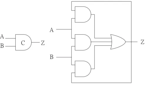
Figure 3.5 shows the 2-input dual-rail AND gate composed of four C-elements and one or gate. The outputs are valid when all inputs are valid data. We construct other logic gates, OR, XOR, which are needed with same concept. Table 3.4 is the truth table of 2-input dual-rail AND gate.
din1.f C din1.t din2.f dinf.t out.f out.t C C C
Figure 3.5 The 2-input dual-rail AND Gate din1.t din1.f din2.t din2.f out.t out.f
0 1 0 1 0 1
0 1 1 0 0 1
1 0 0 1 0 1
1 0 1 0 1 0
30
3.3.3 C-Latch
Our pipeline latches (Figure 3.6) are made up of C-element with reset. C-latch are designed the same as Muller pipeline design. It keeps the valid data until the acknowledge signal changed from 1 to 0. When the valid data in C-latch is delivered to next pipeline stage, it sends a acknowledge signal, 1, to previous stage. Then, current stage can start a new process. On the other hand, if empty token is delivered, it sends an acknowledge signal, 0, to previous stage. These latches in pipeline have 50% utilization at most due to four-phase protocol.
ACK_IN
ACK_OUT
Din.t
Din.f
Out.t
Out.f
C
C
Figure 3.6 C-Latch3.3.4 DeMUX and MERGE
Each datapath may have different works to do. In order to improve the utilization of function unit, there are several datapath executed in parallel possibly. In synchronous circuit design, it uses a multiplexer to select the result to output. In DI circuits of asynchronous processor design, it could be designed that operations are executed in different length of time, and maybe the function units are not used. DeMUX and MERGE are used for this situation. It
31
can select one of datapaths between DeMUX and MERGE, and the other function units which are not in selected datapath are idle. Therefore, the idle function units are not active. It can save power in the way. Figure 3.7 shows the DeMUX and MERGE. The DeMUX consists of two C-elements, and MERGE is made of OR gate because only one function block is active and the other function block will be NULL.
Function block Function block Din Sel.t Sel.f C C DeMUX MERGE Dout
Figure 3.7 DeMUX and MERGE
3.3.5 Memory Interface
In our two-way VLIW microprocessor implementation, we use the traditional synchronous memory. Because the pipeline architecture is based on asynchronous circuit design, it needs an interface to communicate between the function unit and synchronous memory. The Memory Interface converts dual-rail form into single-rail form (Figure 3.8). It sends a request signal to synchronous memory when the read signal and address of LDST function unit arrive. The data will send back to LDST function unit in delay_1. On the other
32
hand, the write operation uses the same conception. Note that read and write operation are not worked at same time.
Addr.t[0] Addr.f[0] Addr.t[31] Addr.t[31] Addr[0] Addr[31] Delay 1 C Memory
Interface Sync MEM
Read_data[0] Read_data[31] Read_data.f[0] Read_data.t[0] Read_data.f[31] Read_data.t[31] LDST EX2 Write_data.f[0] Write_data.t[0] Write_data.f[31] Write_data.t[31] Write_data[0] Write_data[31] C
W_Done.f Delay 2 Write_REQ
Read_REQ C Read_Req.t Read_Req.f C W_Done.t
33
3.3.6 MAC and LDST function units
Figure 3.9 and Figure 3.10 show the block diagram of MAC and LDST function. There are two ALUs, barrel shifters, signed multipliers, pack unit, unpack unit, and unsigned dividers. The ALU can perform common arithmetic, logic, and SIMD operations. Multiplier can accept two 16 bits inputs, and then, generates a 32 bits long product. It is based on shift and add algorithm and constructed of four ripple-carry-save adders. Each ripple-carry-save adder is made up by n+1 full adders (n: wide of input). The last two full adders work for signed bit, and pass to next stage. In this way, we avoid extending the input to 32 bits long to ensure correct product.
Memory
Interface
Barrel Shift
Multiplier/
Divider
ALU
LDST function unit
Pack/Unpack
34
MAC
Barrel Shift
Address generator
Multiplier/
Divider
40-bit Accumulator RegisterALU
MAC function unit
Pack/Unpack
Figure 3.10 Block diagram of MAC function unit
Pack and Unpack unit are used for PACK and UNPACK instructions as introduced in section 3.2. In Figure 3.11, Pack unit consists of two multiplexers. According to the first half of funt field of PACK instruction, Rs.H or Rs.L will be packed into Rd.H. On the other hand, the last half of funt field of PACK instruction decides Rt.H or Rt.L to be packed into Rd.L. Unpack unit consists of four multiplexers (Figure 3.12). It unpacks the 16-bit data in Rd.H into Rs.H or Rs.L (Rd.L into Rt.H or Rt.L). Because our design is based on dual-rail data encoding, one half of Rs (Rt) will be valid, and the other have to get from Rs (Rt). We can perform complete detection with this way. For example, if Rd.H is unpacked into Rs.H, the data in Rs.L still stay in its field.
35 1 1 0 0 Rd.H Rd.L Rs.H Rs.L Rt.H Rt.L
Figure 3.11 Pack unit
Rd.H Rd.L Rd.H Rd.L Rs.H/Rt.H Rs.L/Rt.L 1 1 1 1 0 0 0 0 Rs.H/Rt.H Rs.L/Rt.L
Figure 3.12 Unpack unit
3.4 PIPELINE ARCHITECTURE
There are six stages in our pipeline architecture: PF (Prefetch), DP (Dispatch), ID/OF (Instruction Decode and Operand Fetch), EX1 (Execute 1), EX2 (Execute 2), and WB (Write Back). In this section, they are described in details, and the solution of data hazards and control hazards are going to be introduced. Data hazards are solved in ID/OF stage and control hazards in IF stage. Figure 3.13 shows our two-way VLIW pipeline architecture. Because our microprocessor is a two-way VLIW design, we name the path which is responsible for data transference with data memory “path A” and another “path B” in order to describe the features and function of datapath conveniently.
36 Instruction Memory Date Memory
IF
IDP
ID/
OF
EX1
Memory interface PC RegistersEX2
WB
AccumulatorEX1
EX2
WB
MAC FU
LDST FU
Figure 3.13 Pipeline Architecture
3.4.1 PF and DP Stage
The instruction packet packs extra NOP instruction if the instructions in same packet could not execute in parallel. But it may waste too memory space to store these instruction packets. In most VLIW processor, there are some instruction compression mechanisms to solve this problem. In our PF stage, the 64-bit instruction packet is fetched from instruction memory. Then, the next stage (DP stage) decompresses this instruction packet. If the two instructions in same packet could be executed in parallel, they are separated into different execution order.
Furthermore, we solve the control hazard in DP stage. Because the utilization of pipeline is 50%, we could pass one instruction at most. If the BEQ/BNEQ is fetched and executed in
37
EX1 stage, the stall mechanism works in DP stage. After BEQ/BNEQ finishes its own job in EX1 stage, it sends the correct target address to PC register. Then, the PF stage could fetch the correct instruction packet.
3.4.2 ID Stage
The source operand which is used by instruction is fetched in this stage. It is also responsible to generate control signals for instruction. The control signals are decoded in Instruction Decoder unit. The outputs of Instruction Decoder include the control signals of ID/OF, EX1, EX2, and WB stage. The control signals of EX1, EX2, and WB stage are delivered stage by stage (Figure 3.14). There are two Instruction Decodes and two sets of control path due to two-way VLIW design, and used for MAC function unit and LDST function unit respectively.
The two datapaths share the Register Bank. Source operands in different datapath can be fetched simultaneously. The ID stage consists of two parts (Figure 3.15), Instruction Decoder and Register Bank which is described in the following. Moreover, there are two paths between DeMUX and MERGE, one is bypass line for NOP instruction, and the other is used for common instruction.
38 Register Bank EX1 Instruction Decoder Instruction Decode Reg_control Reg_control EX2 WB WB control EX2 control EX1 control EX1 control WB control EX2 control EX2 control WB control WB control WB control EX2 control EX1 control WB control EX2 control WB control EX1 control EX2 control WB control
Figure 3.14 Control Path
Register Bank
Write back 1 Write back 2
dst dst DeMUX DeMUX MERGE MERGE sel sel Instruction Decoder Instruction Decoder ack ackout ack ack ackout ack
39
3.4.2.1 Register Bank
Figure 3.16 shows the block diagram of Register Bank. It is consists of Operand Decoders, Lock Queue, and Register file.
Operand Decoder: It is responsible to convert operand register number into a 32-bit representation (1-of-32), which is used for selecting which register can be read. For example, the operand register number, 00010, is decoded to 00000000000000000000000000000100, it means the $g2 is to read.
Register file: It has six read ports and two write ports to serve two datapaths. The operands include operand A, operand B (the second operand of R-type instruction), immediate value (the second operand of I-type instruction from the imm field of instruction).
Register file
Operand Decoder OperandsWrite data _1
Lock Module
Write data _2
Operand Decoder Operands40
Lock Module: The pipeline may have data hazard caused by two successive instructions, if the source operand of the second instruction is the result of the first instruction. In this situation, it may occur RAW hazard (read after write) if the result does not be written before the second instruction gets it. Figure 3.17 shows the block diagram of Lock Module. It is similar to Lock FIFO of Asynchronous Microprocessor designed by N.C Paver [2]. We use a queue to store the destination register number and the concept of implement is also similar to Lock FIFO. We modify the design of Lock FIFO simply to suit our two-way VLIW architecture.
Lock Queue
Rd push Ack pre_stage pop Rs Rt Rs1_E Rt1_E Write_EOperand read done Ack from EX_latch
c
Push done
Converter Converter
Converter C
Figure 3.17 Block diagram of Lock Module
The three converter units in Figure 3.17 are dual-rail to single-rail converter. (There are same set of elements and control path at another datapath.) When Rs (Rt, Rd) is valid, the operand register number is converted from dual-rail to single-rail, and control unit send a request to Lock Queue to check whether it is stalled by previous instruction or not. Lock
41
Queue is used for solving RAW hazard. It stores information of destination register, and deletes the information of destination register after the results from WB stage are written into destination register. The instruction is stalled in ID stage if the RAW hazard occurs. There are two Lock Queues in each datapath. They store their destination register number individually. When instruction is executed in Lock Queue, not only it have to check its own Lock Queue, but the another Lock Queue in anther datapath. Therefore, one of datapath may be stalled by another. For example, there are two successive instruction packets are executed in parallel, and their operands are list as following:
ADD $g4, $g1, $g0 … (1), ADD $g2, $g1, $g0 … (2) ADD $g5, $g2, $g0 … (3), ADD $g6, $g4, $g0 … (4)
Instruction (3) and (4) are executed follow (1) and (2). After Instruction (1) and (2) finished the work in ID/OF stage, the contents of Lock Queue for each datapath is
LQ1 LQ2
$g4 $g2
Instruction (1) is executed in parallel with (2), and (3) is executed in parallel with (4). Instruction (3) is stalled by (2) because one source operand ($g2) comes from (2), and (2) has not finished. Instruction (3) and (4) cannot store their destination register number to Lock Queue because they are stalled by Instruction (2) and (1), respectively. Instruction (3) and (4)
42
cannot store their destination register number until they complete the read operand operation. After (1) and (2) finish, the Lock Queues are updated:
LQ1 LQ2
$g5 $g6
At this time, instruction (3) and (4) are not stalled anymore. The information of destination register cannot be pushed into Lock Queue until the operands are fetched from register file. This policy can make sure deadlock never occur. For example, the executing instruction is “ADD $g3, $g3, $g1”, one of source operand ($g3) and the destination register ($g3) are the same. The deadlock may occur in ID stage if the information of the destination register is pushed into Lock Queue before the two operands are fetched from register file.
3.4.3 EX Stage
The EX stage is responsible for computations and returning the result to register file, and it is separated into three stages, EX1, EX2, and WB stage. Each datapath has individual function unit as shown in Figure 3.18 (a) and Figure 3.18 (b) due to two-way VLIW design, and works individually. They have to wait for each other. Then, an acknowledgement signal will be sent to previous stage. The one of datapath is responsible for MAC and branch instruction, and the another is responsible for Load and Store instruction. The basic arithmetic operations can be executed in both datapaths. The three stages are described in following. The
43
DeMUX and MERGE pairs described in section 3.3.4 are used for selecting data flow in each stage. If there is not work in execution stage, they can be bypassed. Figure 3.18 (a) shows the block diagram of Path A, and Figure 3.18 (b) shows the block diagram of Path B.
ALU 16 X 1 6 D ua l R ail M ult ip lie r/D iv id er Barrel Shifter MEM Interface Write Data Address Read Data Latch 1MUX2 Latch Latch Sh ift R es ult Ba se R eg ite r op A W rit e D ate 1DeMUX2 1 MUX2 Write To Register ack ack 1MUX 1MUX Fraction 1 MUX2 op B Sign Extend Sh ift A m ou nt Data Memory W_Don e 3 ack ack C Ack_MAC Ack_LDSD To EX2/WB Latch in Path B
Path A
EX1
EX2
WB
44
EX1
EX2
WB
40 bits Adder MAC AC C MERGE EX1/EX2 Latch Latch W rit e Bu s MUX 16 X 16 Dual Rail Multiplier/Divider DeMUX EX2/WB Latch AL U O ut ack ack ack ack Sign Extend Acc Register C Ack_MAC Ack_LDSD Sign Exten d 1 MUX2 Barrel Shifter O pe ra nd B 13 bits Adder PC V alu e Sign Exte nd 1MU X 1 MUX $ra PC_out AL U O ut ALU Sh ift er O ut 1 MUX PC Value E_0 To EX2/WB Latch in Path APath B
Figure 3.18 (b) Path B3.4.3.1 EX1 Stage
The instruction reads the contents of two registers and immediate value from pipeline latches. It is delivered to correct path by DeMUX. In path A, there are three portions. It can perform multiplication, division, shift, and arithmetic operations. The ALU is used for general arithmetic operations and calculating memory address of load and store instructions.
45
In path B, there are four portions. It can also perform multiplication, division, and shift. In addition, there are sign-extended unit and address generator. The branch operation can calculate the target address in this stage, and then, the target address is passed to DP stage to solve control hazard caused by branch instruction.
3.4.3.2 EX2 Stage
In path A, it is separated into two parts. The first is data transfer, and the other is data pass. Load and store instructions can fetch and store data with memory via memory interface. On the other hand, the general instructions which do not need to read or write memory will do nothing in this stage.
In path B, there are two portions, MAC and ALU. The MAC operation reads the contents of 40-bit accumulator register in this stage. Then, the outcome is written into accumulator at next stage. So we can ensure correctness of accumulator. The valid token is bypassed in this stage if the executing instruction is branch instruction which completes its job at previous stage.
3.4.3.3 WB Stage
WB stage is the final stage of our pipeline. It is responsible for saving the result back to register file according to the destination register number. If instructions have finished in previous stage, for example, “SW Rd, Rs, imm”, it has nothing to do in this stage. For multiply-accumulates instruction, the output of MAC unit is written into 40-bit accumulator
46
in this stage. The value in 40-bit accumulator could be moved into register with ACCLDH and
ACCLDL in order to support other application. Because our pipeline architecture is based on
4-phase dual-rail handshaking protocol, the accumulator is read or written at different time due to half of utilization of pipeline stage. Finally, the datapath which finish its own job early has to wait for another only in this stage.
47
CHAPTER 4 SIMULATION
4.1 TESTING ENVIRONMENT
We use ModelSim 6.0 to verify the correctness of the functionally. In addition, we also synthesized our design with Design Compiler. They are synthesized by TSMC .13μ m process library. The result of area and timing report are described in the following sections. Figure 4.1 shows the waveform of the function simulation.
48
4.2 AREA SIMULATION
With TSMC .13μ m processes, the area report of each stage of our two-way VLIW processor is shown in Table 4.1. Table 4.1 shows the area of each pipeline stage except PF and DP stage. Table 4.2 shows the area of register bank.
(μ ㎡) ID/OF EX1 EX2 WB Total
LDST 174762.6 (43.5%) 66402.3 (16.5%) 5560.6 (1.4%) 531.3 (0.13%) 401581.1 (100%) MAC 41518.4 (10.3%) 55644.2 (13.9) 2742.9 (0.68%) Table 4.1 The area report of each stage
Lock Module Register File 11116.3(μ ㎡) 57450.2 (μ ㎡) Table 4.2 The area report of register bank
4.3 TIMING SIMULATION
With TSMC .13μ m processes, the timing report of each stage of our two-way VLIW processor is shown in Table 4.2. The EX1 stages have longer latency than other stages
49
because the multiplier and divider are executed in this stage. In EX2 stage, we ignore the memory latency because the memory is based on synchronous circuit design.
(ns) ID/OF EX1 EX2 WB
LDST
22.62
65.18 10.48 2.8
MAC 65.75 61.23 2.11
50
CHAPTER 5 CONCLUSION AND FUTURE
WOROKS
In this thesis, we have implemented a two-way VLIW processor based on asynchronous circuit design with four-phase dual-rail handshaking protocol. It is a six-stage pipeline architecture. Each stage can execute in variable length of time due to asynchronous circuit nature. It can reduce the instruction memory space via instruction compression. In addition, it also supports SIMD application and multiplier-accumulate operation. There are nine instructions for SIMD application. Moreover, the DeMUX and MERGE can be used to improve the performance. The datapath can be separated into several parts. If the function units between DeMUX and MERGE are not used, the DeMUX will bypass these function units.
In our datapath design, it has two read ports and one write ports for each datapath. We could try to increase the read and write ports in register file in order to improve the performance of SIMD application because the Unpack instruction has to perform twice to unpack a 32-bit value to the destination register. More important, we wish this light-weight asynchronous core could be used to construct a multi-core processor via interconnection network in the future.
51
Reference
[1] Jens Sparso and Steve Furber, Principles of Asynchronous Circuit Design, Kluwer Academic Publisher, 2001.
[2] N.C. Paver, “The Design and Implementation of an Asynchronous Microprocessor,” Ph.D thesis, Department of Computer Science, The University of Manchester, 1994
[3] S.B. Fuber, P. Day, J.D. Garside, S. Temple, J. Lin, and N.C. Paver, “AMULET2e: An Asynchronous Embedded Controller,” in the third International Symposium on Advanced Research in Asynchronous Circuits and Systems, ASYNC97, pp.243-256, 1997
[4] S.B. Furber, J.D. Garside, D.A. Gilbert, “AMULET3: A High-Performance Self-Timed ARM Microprocessor,” in International Conference on Computer Design: VLSI in Computers and processors, ICCD ’98, pp.247-252, 1998
[5] C.J Chen, W.M. Cheng, H.Y. Tsai, J.C. Wu, “A Quasi-Delay-Insensitive Mircoprocessor Core Implementation for Microcontrollers,” Journal of Information Science and Engineering, Vol. 25, No.2, Mar. 2009, pp543-557
[6] Hung-Yue Tsai, “A Self-timed Dual-rail Pipelined Microprocessor Implementation,” National Chiao Tung University, 2007
[7] T. Nanya, et.al, “TITAC: Design of a Quasi-Delay-Insensitive Microprocessor,” IEEE Design & Test of Computer, Summer 1994, pp. 50-63
[8] A. Takamura, et.al, “TITAC-2: A 32-bit Asynchronous Microprocessor based on Scalable-Delay-Insensitive Model,” in Proceedings of the International Conference on Computer Design, Oct. 1997, pp.288-294
[9] T. Kumura, M. Ikekawa, M. Yoshida, and Ichiro Kuroda, “VLIW DSP for Mobile Applications,” Signal Processing Magazine, IEEE, Vol. 19, Issue 4, pp. 10-21, 2002 [10] TMS320C55x Technical Overview, Texas Instruments Inc., Literature Number: SPRU393, 2000, http://www.ti.com
52
[11] TMS320C64x DSP Library Programmer’s Reference, Texas Instruments Inc., Literature Number: SPRU565B, 2003, http://www.ti.com
[12] T. Kumura, D. Ishii, M. Ikekawa, I. Kuroda, and M. Yoshida, “A low-power
programmable DSP core architecture for 3G mobile terminals,” in Proc. IEEE int. Conf, Acoustics, Speech, and Signal Processing, Vol. 2, pp.1017-1020, 2001
[13] T. Chen, R. Raghavan, J.N. Dale, E. Iwata, “Cell Broadband Engine Architecture and its first implementation- A performance view, ” IBM Journal of Research and Development, Vol. 51, Issue: 5, pp.559-572, Sept. 2007
[14] G. Hinton, D. Sager, M. Upton, D. Boggs, D. Carmean, A. Kyker, P. Roussel, “The Mircoarchitecture of the Pentium 4 Processor”, Intel Technology Journal, Vol. 5, Issue: 1, 2001, http://www.intel.com