氧化鋅量子點尺寸對能帶變化及電子-聲子交互作用之影響
57
0
0
全文
(2) 氧化鋅量子點尺寸對能帶變化及電子-聲子交互作用 之影響. Size dependence of band gap variation and electron-phonon coupling in ZnO Quantum Dots 研 究 生:林國峰. Student: Kuo-Feng Lin. 指導教授:謝文峰 教授. Advisor: Dr. Wen-Feng Hsieh. 國立交通大學 光電工程研究所 碩士論文 A Thesis Submitted to Institute of Electro-Optical Engineering College of Electrical Engineering and Computer Science National Chiao Tung University in Partial Fulfillment of the Requirements for the Degree of Master in Electro-optical Engineering June 2005 Hsin-chu, Taiwan, Republic of China. 中華民國九十四年六月 B.
(3) 氧化鋅量子點尺寸對能帶變化及電子-聲子交互作用之影響. 研究生: 林國峰. 指導教授: 謝文峰 教授. 國立交通大學光電工程研究所. 摘要 我們成功地利用溶膠-凝膠製造氧化鋅量子點,再利用改變溶液濃 度、加熱速率以及反應時間等方法去控制氧化鋅量子點的尺寸大小。 室溫螢光及吸收光譜觀察到明顯的藍位移現象,並與 effective mass model 的弱侷限效應計算的結果相符合。室溫螢光與吸收光譜譜峰之 間距隨氧化鋅量子點的尺寸變小而變大的現象,也顯示氧化鋅量子點 存在量子侷限效應。最後,我們由 Raman 光譜發現隨著氧化鋅量子 點的尺寸變小而造成能量守恆的鬆弛及電子-聲子交互作用的能量變 小的現象。. I.
(4) Band Gap Variation of Size-Controlled ZnO quantum dots synthesized by sol-gel method. Student: Kuo-Feng Lin. Advisor: Prof. Wen-Feng Hsieh. Institute of Electro-optical Engineering National Chaio Tung University. Abstract ZnO quantum dots were successfully synthesized by a simple sol-gel method. The average size of quantum dots can be tailored under several well-controlled methods which are solution concentration, heating rate and aging time. Size-dependent blue shifts of photoluminescence and absorption spectra reveal the quantum confinement effect.. The band gap enlargement is in agreement with the. theoretical calculation based on the weak confinement of effective mass model. Furthermore, we observed increase of the size-dependent Stokes shift of the photoluminescence peak relative to the absorption onset as the particle size decreases. Finally, we observed the results that energy conservation was relaxed and electron-phonon coupling energy was decreasing with decreasing quantum dots size by Raman spectra.. II.
(5) 誌謝 時間的流逝真是快速,轉眼間我已經是一個即將畢業的碩士生了。 回想過去這兩年的日子裡,是多麼的辛酸血淚,多麼的艱辛。不過以 上在我們實驗室裡是看不到的,因為實驗室裡時時刻刻充滿著歡笑與 快樂的呀! 學習的過程是痛苦的,但是學習結果是甜美的。然而由於老師及實 驗室的學長們的指導使得我在學習過程中可以輕鬆自在。因此,我特 別要感謝我的指導老師謝文峰教授,在這兩年來在我課業、實驗以及 待人處世上的指導及教誨。特別感謝政哥、鄭信民學長在於我實驗上 以及課業上的幫助跟指教(對這兩位學長深深感到歉意,每次有問題 及需要幫忙時都找你們,害得你們跟女友相處時間無形中變少了); 也要感謝黃董、維仁、楊松精神及技術性上的指導。還有實驗室內可 愛的學弟妹們,使得我在這兩年內的生活多采多姿,真是太感謝你們 了。還有那些跟我共存亡的同儕們(雖然大部分都還是自顧自的),我 們是共同經歷生死關卡的好同學、好朋友。在此我祝福你們鵬程萬 里、事事如意。 最後感謝國科會計畫 NSC-93-2112-M-009-035 對於此研究的支持 以及贊助。 國峰 于 九十四年六月八日 III.
(6) Contents Abstract (in Chinese). Ⅰ. Abstract (in English). Ⅱ. Acknowledgements. Ⅲ. Contents. Ⅳ. List of Figures. Ⅵ. Chapter 1 Introduction. 1. Chapter 2 Theoretical background. 3. 2.1 Sol-gel method. 3. 2.2 Quantum effect. 5. 2.2.1 Quantum confinement effect. 5. 2.2.2 Density of states. 8. 2.3 X-ray diffraction. 10. 2.3.1 Lattice parameters. 10. 2.3.2 Debye-Scherer formula. 10. 2.4 Photoluminescence characterization. 13. 2.5 Raman spectroscopy. 14. Chapter 3 Experiment detail. 20. 3.1 Sample preparation. 20. 3.2 Microstructure and optical properties analysis. 21. 3.2.1 X-ray diffraction. 21 IV.
(7) 3.2.2 Optical absorption spectra. 21. 3.2.3 Photoluminescence system. 22. 3.2.4 Raman system. 23. Chapter 4 Results and discussion. 29. 4.1 HRTEM and X-ray diffraction measurement. 29. 4.2 Absorption and Photoluminescence Spectra. 30. 4.3 Raman spectra analysis. 32. Chapter 5 Conclusion and perspective. 44. 5.1 Conclusion. 44. 5.2 Perspective. 44. References. 46. V.
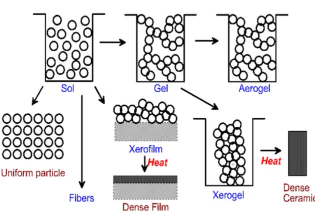
(8) List of Figures Fig. 2-1 Schematic of the rotes that one could follow within the scope of sol-gel processing. 15. Fig. 2-2 Geometry used to calculate density of states in three, two and one dimensions. 16. Fig. 2-3 Variation in the energy dependence of the density of states. 17. Fig. 2-4 The crystalline planes of the materials. 18. Fig. 2-5 A pair excitation in the scheme of valence and conduction bands 18 Fig. 2-6 Visualization of an exciton bound. 19. Fig. 2-7 The picture of anti-Stokes and Stokes scattering processes. 19. Fig. 3-1 Experiment equipment used for fabricating ZnO quantum dots. 24. Fig. 3-2 XRD ω-2θ scans geometry for ZnO nanoparticles. 26. Fig. 3-3 PL detection system. 27. Fig. 3-4 Raman detection system. 28. Fig. 4-1 HRTEM image and size distribution of the ZnO QDs fabricated using 0.06M Zn(OAc)2. 35. Fig. 4-2 XRD profiles of the ZnO QDs prepared with various concentrations36 Fig. 4-3 PL and absorption spectra near the band edge of various sizes of ZnO QDs. 37. Fig. 4-4 The dependence of the band gap enlargement and exciton binding VI.
(9) energy versus the ZnO QDs diameter. 38. Fig. 4-5 The dependence of the Stokes shift versus the ZnO QDs diameter39 Fig. 4-6 PL spectra of various aging time at 0.08M concentration. 40. Fig. 4-7 PL spectra of various heating rate at 0.1M concentration. 40. Fig. 4-8 Raman spectra of various ZnO QD. 42. Fig. 4-9 Resonant Raman Spectra of various ZnO QDs. 43. VII.
(10) Chapter 1 Introduction Semiconductor. nanoparticles. have. attracted. significant. attention. for. their. distinguishable role in fundamental studies and technical applications, [1,2] mainly due to their unusual photonic characteristics, which have been demonstrated in the recent years.. Zinc oxide (ZnO) is a versatile material that has achievable. applications in photo-catalysts, varistors, sensors, piezoelectric transducers, solar cells, transparent electrodes, electroluminescent devices, and ultraviolet laser diodes, as a result, it stimulates fairly extensive researches.[3-13] Compared with other wide band gap materials, ZnO has a very large exciton binding energy of 60 meV which results in efficient excitonic emission at room temperature. It is known that ZnO nanocrystals or quantum dots (QDs) have superior optical properties to the bulk crystals owing to quantum confinement effects.. In the past decade, various methods. have been employed to produce ZnO quantum QDs.[14–21] For instance, Guo et al.[15] experimentally established that the third-order nonlinear susceptibility of ZnO nanoparticles is almost 500 times larger than that of bulk ZnO.. Vanmaekelbergh and. co-workers[22] discovered the optical transitions in artificial atoms consisting of one to ten electrons occupying the conduction levels in ZnO nanocrystals. Fonoberov et al.[23] have theoretically investigated that, depending on the fabrication technique and ZnO QD surface quality, the origin of UV photoluminescence (PL) in ZnO QDs is either recombination of confined excitons or surface-bound ionized acceptor–exciton complexes.. More and more unique behaviors are continuously being explored.. Understanding the electronic and optical properties of ZnO QDs and nanoparticles is important from both fundamental science and proposed photonic applications points 1.
(11) of view. Absorption spectra were general widely used to investigate the band edge emission from ZnO QDs.[14-20]. However, direct observation of the band gap. variation upon particle size from PL is relatively rare.[21] In this thesis, we show growth of high-quality ZnO QDs by a simple sol-gel method.. The average size of. nanoparticles can be tailored by the appropriate concentration of zinc precursor, aging time and heating rate. Furthermore, size-dependent PL and absorption spectra are carefully discussed and compared with the theoretical calculation using the effective mass model.. We will examine the variable results of Raman spectra with adjustable. ZnO nanoparticle size.. 2.
(12) Chapter 2 Theoretical background 2.1 Sol-gel method A colloid is a suspension in which the dispersed phase is so small (~1-1000nm) that gravitation force is negligible and interactions are dominated by the short-range forces, such as der Waals attraction and surface charge. The precursors were mixed together and heated at high temperature. This procedure has to be repeated several times until a homogeneous product is obtained. transformed into the desired shape.. Then, the materials have to be. Sol-gel synthesis has two ways to prepare. solution. One way is the metal-organic route with metal alkoxides in organic solvent; the other way is the inorganic route with metal salts in aqueous solution.. It is much. cheaper and easier to handle than metal alkoxides, but their reactions are more difficult to control.. The metal-organic route uses metal alkoxides in organic solvent.. The inorganic route is a step of polymerization reactions through hydrolysis and condensation of metal alkoxides M(OR)Z, where M = Si, Ti, Zr, Al, Sn, Ce, and OR is an alkoxy group and Z is the valence or the oxidation state of the metal.. First,. hydroxylation upon the hydrolysis of alkoxy groups:. M − OR + H 2 O → M − OH + ROH. (2-1). The second step, polycondensation process leads to the formation of branched oligomers and polymers with a metal oxygenation based skeleton and reactive residual hydroxyl and alkoxy groups.. There are 2 competitive mechanisms:. Oxolation: formation of oxygen bridges:. M − OH + XO − M → M − O − M + XOH ,. 3. (2-2).
(13) The hydrolysis ratio (h = H2O/M) decide X=H (h>>2) or X=R (h<2). Olation:. formation of hydroxyl bridges when the coordination of the metallic center. is not fully satisfied (N - Z > 0):. M − OH + HO − M → M − (OH ) 2 − M , where X=H or R.. (2-3). The kinetics of olation is usually faster than those of oxolation.. Figure 2-1 presents a schematic of the routes that one could follow within the scope of sol-gel processing [24].. A sol is a colloidal suspension of solid particles in a liquid.. An aerosol is a colloidal suspension of particles in a gas (the suspension may be called a fog if the particles are liquid and a smoke if they are solid) and an emulsion is a suspension of liquid droplets in anther liquid. All of these types of collides can be used to generate polymers or particles from which ceramic materials can be made. In the sol-gel process, the precursors (starting compounds) for preparation of a colloid consist of a metal or metalloid element surrounded by various ligands.. For example,. an alkyl is a ligand formed by removing one hydrogen (proton) from an alkane molecule to produce, for example, methyl (‧CH3) or ethyl (‧C2H5).. An alcohol is a. molecule formed by adding a hydroxyl (OH) group to an alkyl (or other) molecule, as in methanol (CH3OH) or ethanol (C2H5OH). Metal alkoxides are members of the family of metalorganic compounds, which have an organic ligand attracted to a metal or metalloid atom.. Metal alkoxides are. popular precursors because they react readily with water. The reaction is called hydrolysis, because a hydroxy ion becomes attached to the metal atom.. This type of. reaction can continue to build larger and larger molecules by the process of polymerization.. A polymer is a huge molecule (also called a macromolecule). formed from hundreds or thousands of units called monomers.. If one molecule. reaches macroscopic dimensions so that it extends throughout the solution, the 4.
(14) substance is said to be gel. The gel point is the time (or degree of reaction) at which the last bound is formed that completes this giant molecule.. It is generally found. that the process begins with the formation of fractal aggregates that they begin to impinge on one anther, then those clusters link together as described by the theory of percolation.. The gel point corresponds to the percolation threshold, when a single. cluster (call the spanning cluster) appears that extends throughout the sol; the spanning cluster coexists with a sol phase containing many smaller clusters, which gradually become attached to the network. Gelation can occur after a sol is cast into a mold, in which it is possible to make objects of a desired shape.. 2.2 Quantum effect During the last decade, the growth of low-dimensional semiconductor structures has made it possible to reduce the dimension from three (bulk material) to the quasi-zero dimensional semiconductor structures usually called quantum dots (QDs).. In these. nanostructures the quantum confinement effects become predominant and give rise to many interesting electronic and optical properties. The electron energy becomes quantized and depends on the dot size.. The band gap and density of states (DOS). associated with a quantum-structure differs from that associated with bulk material, determined from the magnitude of the three-dimension wave vector.. 2.2.1 Quantum confinement effect Models explaining the confinement of charged particles in a three-dimensional potential well typically involve the solution of Schrodinger’s wave equation using the Hamiltonian[25] 5.
(15) H =−. h2 2 h2 2 ∇e − ∇ h + V0 + U 2me 2me. (2-4). Variation between treatments generally originates from differences in expressions assigned to V0 which normally will is accompanied by the Coulombic interaction term U. Boundary conditions are imposed forcing the wave functions describing the carriers to zero at the walls of the potential well.. Two regimes of quantization are. usually distinguished in which the crystallite radius R is compared with the Bohr radius of the excitons or related quantities:. weak confinement: R ≥ a B and. strong confinement: R < a B . In the first case crystallite radius is larger than the exciton. As a consequence, the motion of center of mass of the exciton is quantized while the relative motion of electron and hole given by the envelope function φ (re − rh ) is hardly affected.. In. the second case the Coulomb energy increases roughly with R-1, and the quantization energy with R-2, so that for sufficiently small values of R one should reach a situation where the Coulomb term can be neglected.. 2.2.1.1 Weak confinement [26] Coulomb-related correlation between the charged particles handled through the use of a variational approach involving higher-order wave function of the confined particles, and we can not neglect the electron hole Coulomb potential.. The. Schrodinger equation may be written as (−. h2 h2 − )∇ 2 Ψ + [V0 + U (re − rh )]Ψ = Et Ψ 2 me 2m h. We take r = re − rh and R =. me re + mh rh , then the equation becomes me m h. h2 2 h2 2 [− ∇R − ∇ r + V ( R) + U (r )]Ψ = Et Ψ 2M 2µ 6. (2-5).
(16) me m h , and E t as the total energy of the system. If we me + m h. with M = me + mh , µ =. take Ψ = φ ( R )ϕ ( r ) and consider Coulomb interaction first, then we get [−. h2 2 ∇ R + V ( R)]φ ( R) = E c Ψ , 2M. h2 2 [− ∇ r + U (r )]ϕ (r ) = ( Et − Ec )ϕ (r ) = Eexϕ (r ) . 2µ Here Eex is resulting from the inclusion of Coulomb interaction. Then we consider the confinement potential V ( R ) = 0, R ≤ a V ( R ) = ∞, R > a. .. Thus, the energy is E cn =. h 2π 2 n 2 , n = 1,2,3..... 2Ma 2. and the absorption energy of a photon is hω 0 = Et = E c − E ex = E g +. h 2π 2 − E ex 2Ma 2. (2-6). with M = me + mh as the total mass of the electron and hole.. 2.2.1.2 Strong confinement The size quantization band states of the electron and hole dominates for the kinetic energies of electron and hole are larger than the electron-hole Coulomb potential, and the effect of the Coulomb attraction between the electron and hole can be treated as a perturbation.. Then the Schrodinger equation becomes (−. h2 h2 − )∇ 2 Ψ + V0 Ψ = EΨ . 2me 2me. The potential is defined as V (r ) = 0, r ≤ a V ( r ) = ∞, r > a. and the energy of a electron or hole is. 7.
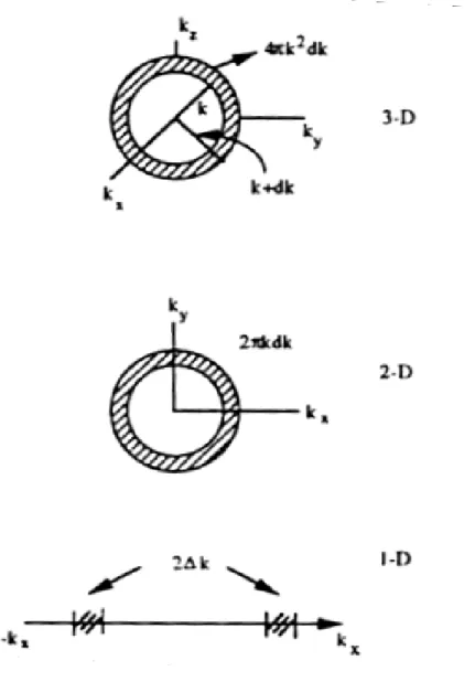
(17) E cn =. h 2π 2 n 2 , n = 1,2,3..... 2m e , h a 2. The absorption energy of a photon is hω 0 = E g + with µ =. 1 h 2π 2 1 h 2π 2 ( ) E + = + g 2a 2 me m h 2a 2 µ. (2-7). me m h as the reduced mass of electron and hole. me + m h. 2.2.2 Density of states (DOS) The concept of density of states (DOS) is extremely powerful. Important physical properties such as optical absorption, transport, etc., are intimately dependent upon this concept.. The density of states is the number of available electronic states per. unit volume per unit energy interval around an energy E.. If we denote the density of. states by N(E), the number of states in an energy interval dE around an energy E is N(E)dE. To calculate the density of states, we need to know the dimensionality of the system and the energy vs. wave vector relation or the dispersion relation that the electrons obey.[27]. 2.2.2.1 Density of state for a three-dimensional system In a three dimension system, the k-space volume between vector k and k + dk is (see Figure 2-2) 4πk2dk. state is 3(2π/L).. We had shown above that the k-space volume per electron. Therefore, the number of states of electron in the region between k. and k+ dk are k 2 dk 4πk 2 dk V = V. 8π 3 2π 2 Denoting the energy and energy interval corresponding to k and dk as E and dE, we 8.
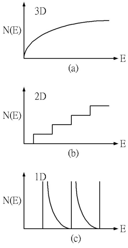
(18) see that the number of electron states between E and E+ dE per unit volume is N ( E )dE = and since E =. k 2 dk 2π 2. h2k 2 , then the equation becomes 2m 3. k 2 dk =. 1. 2m 2 E 2 dE , h3. which gives 3. N ( E )dE =. 1. m2E 2 2π 2 h 3. dE.. We must remember that the electron can have two states for a given k-value since it can have a spin state of s=1/2 or -1/2. 3. N (E) =. Accounting for spin, the density of states is. 1. 2m 2 E 2 . π 2h3. 2.2.2.2 Density of states for lower-dimensional systems If we consider a 2-D system, a concept that has become a reality with use of quantum wells, similar arguments tell us that the density of states for a parabolic band is N (E) =. m . πh 2. Finally in a 1-D system, or “quantum wire”, the density of states is 1. N (E) =. 2m 2 E πh. −. 1 2. .. We notice that as the dimensionality of the system changes, the energy dependence of the density of states also changes.. In three-dimensional systems we. have a E1/2-dependence as shown in Figure 2-3. In 2-D systems there is no energy dependence (Figure 2-3), while in 1-D systems, the density of states has a peak at E=0 9.
(19) (Figure 2-3).. The variations related to dimensionality are extremely important and is. a key driving force to lower dimensional systems.. 2.3 X-ray diffraction 2.3.1 Lattice parameters Most metals exhibit crystalline structures.. The most common types of such. structures are the simple cubic (SC), the face-centered cubic (FCC) and the wurtzite structure, etc.. By diffracting X-rays with a wavelength comparable to the lattice. constant, the lattice constant can be found by means of the diffraction pattern.. For. hexagonal unit cell which is characterized by lattice parameters a0 and c0, the plane spacing equation for the hexagonal structure is:[28] 1 4 h 2 + hk + k 2 l2 = + , ( ) d2 3 a 02 c02 where h, k , l is the Mill’s index. wavelength of x-ray source.. We know the Bragg’s law (λ = 2d sin θ ) , λ is the. So the equation becomes. 1 2 sin θ 2 4 h 2 + hk + k 2 l2 = = + ( ) ( ) λ 3 d2 a 02 c02. (2-8). thus the lattice parameters can be estimated.. 2.3.2 Debye-Scherer formula [29] Consider now the path difference between successive planes when the incident beam remains fixed at the Bragg angle θ as Figure 2-4, but with the diffracted ray leaving at an angle θ+ ∆θ, corresponding to the intensity I in the spectrum line an angular. 10.
(20) distance ∆θ away from the peak.. The path difference between waves from. successive planes is now [30] BC + CE = d sin θ + d sin(θ + ∆θ ). = d sin θ + d sin θ cos ∆θ + d cosθ sin ∆θ with BC and CE being the path differences between the successive incident beams, and d is the interplanar distance. If ∆θ is small, we can write cos∆θ=1 and sin∆θ=∆θ, in which case. BC + CE = 2d sin θ + d∆θ cosθ. = nλ + d∆θ cosθ , where λ is the wavelength of the incident X-ray.. Therefore the phase δ per. interplanar distance is. δ=. 2π. λ. nλ +. = 2 nπ +. 2π. λ. 2π. d∆θ cos θ. d∆θ cos θ .. λ. Since a phase difference of 2nπ produces the same effect as zero phase, we can write the effective phase difference as. δ=. 2π. λ. d∆θ cos θ .. We obtained the result that the distribution of intensity I in a spectrum line a distance R from the grating is effectively ⎛φ ⎞ I =⎜ ⎟ ⎝R⎠. 2. sin 2 sin 2. Nδ 2. δ. 2. and the maximum intensity is 2. I max. ⎛φ ⎞ = ⎜ ⎟ N2, ⎝R⎠. where φ is the amplitude at unit distance from the grating, N is the total number of 11.
(21) grating apertures, and δ is the phase change per aperture; or I I man Since. Nδ sin 2 1 2 . = 2 N sin 2 δ 2. Nδ δ will change much faster than , the sine square function will reach its 2 2. δ. first minimum before. 2. becomes very large.. If we replace sin. Nδ δ by , we will 2 2. get I I max The ratio. I I max. Nδ 2 )2 . =( Nδ 2 sin. will fall to. 1 when 2. Nδ 2 = 1 . Nδ 2 2. sin. The solution to the equation yields the required phase change corresponding to the half maximum. It may be obtained 1 2π N d∆θ cos θ = 1.39 λ 2. or since D=Nd, we have 2 ∆θ =. 0.89λ . D cos θ. The β is taken as the width at half maximum from ∆θ to –∆θ, and. β = 2 ∆θ =. 0.89λ , D cos θ. (2-9). where λ is the wavelength of the x-ray source, and D is the size of the particles.. 12.
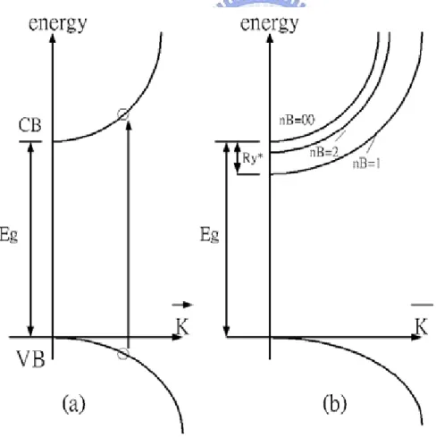
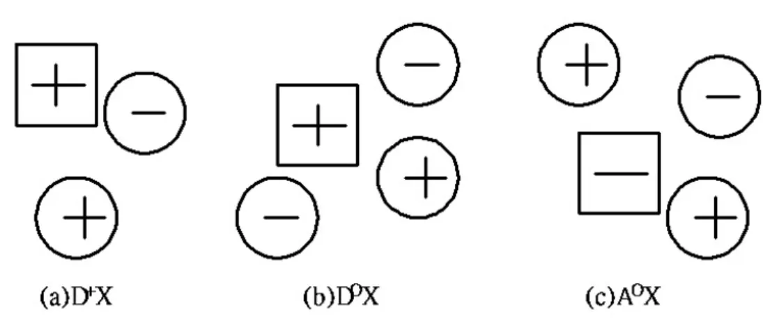
(22) 2.4 Photoluminescence characterization[31] An electron was excited from the valence to the conduction band by absorption of a photon.. In this process, we bring the system of N electrons from the ground state to. an excited state.. We need for the understanding of the optical properties of the. electronic system of a semiconductor is therefore a description of the excited states of the N-particle problem.. The quanta of these excitations are called “excitons”.. Indeed excitons in semiconductors form, to a good approximation, a hydrogen or positroium like series of states below the gap.. For simple parabolic bands and. direct-gap semiconductor one can separate the relative motion of electron and hole and the motion of the center of mass.. This leads to the dispersion relation of. excitons in Figure 2-5. E (n B , K ) = E g −. Ry * h 2 K 2 , + nB 2M. (2-10). where n B = 1,2,3... is the principal quantum number, Ry * = 1.36eV exciton binding energy, M = me + mh and. µ 1 is the m0 ε 2. K = k e + k h are the translational mass. and wave vector of the exciton. The exciton state has an effective Rydberg energy Ry * modified by the reduced mass of electron and hole and the dielectric constant of the medium in which these particles move. complex (BEC).. Some of the defects can bind an exciton resulting in a bound exciton In Figure 2-6 we visualize excitons bound to an ionized donor. (D+X), a neutral donor (D0X), and a neutral acceptor (A0X).. An ionized acceptor. does not usually bind an exciton since a neutral acceptor and a free electron are energetically more favorable.. The binding energy of an exciton (X) is the highest for. a neutral acceptor (A0X complex), the lower for a neutral donor (D0X) and the lower. 13.
(23) still for an ionized donor (D+X).. The binding energy Eb of exciton to the complex. usually increases according to. E Db + X < E Db 0 X < E Ab 0 X . The binding energy is defined as the energetic distance from the lowest free exciton state at k=0 to the energy of the complex.. There is a rule of thumb, known as. Hayne’s rule, which relates the binding energy of the exciton to the neutral complex with the binding of the additional carrier to the point defect.. 2.5 Raman spectroscopy Raman spectroscopy is based on the Raman effect [32].. When photons from a laser. are scattered from a crystal with emission or absorption of phonons, the energy shifts of the photons are small, but can be measured by interferometric techniques. Usually, the phonon wave vectors are very small compared to the size of the Brillouin zone so that the interactions are only with zone center phonon.. Thus, one can have. interaction with either the zone center acoustic phonons or the optical phonons. Once again, one can write the conservation laws for energy and momentum.. It must. be remembered that the wavevectors containing the refractive index n, hω ′ = hω ± hω s (k ) hnq ′ = hnq ± hk + hG ,. where q and q’ are the photon wavevectors in free space.. The upper sign. corresponds to a phonon absorption (the process is called anti-Stokes scattering) while the lower sign corresponds to an emission (Stokes scattering).. Since q and q’ are. very small, G has to be zero. The anti-Stokes and Stokes scattering are shown in Figure 2-7. The anti-Stokes mode is usually much weak than the Stokes mode, and it is Stokes-mode scattering that is usually monitored. 14.
(24) When light is scattered from the surface of sample, the scattered light is found to contain mainly wavelengths that were incident on the sample (Rayleigh scattering) but also different wavelengths at very low intensities (few parts per million) that represent an interaction of the incident light with material.. The interaction with. acoustic phonons is called Brillouin scattering while the interaction with optical is call Raman scattering.. Optical phonons have higher energies than acoustic phonons. giving larger photon energy shifts. Hence Raman scattering is easier to detect than Brillouin scattering.. Subsequently, Raman scattering is a vibrational spectroscopic. technique that can detect both organic and inorganic species and measure the crystalline of solids.. Figure 2-1 Schematic of the rotes that one could follow within the scope of sol-gel processing.. 15.
(25) Figure 2.2 Geometry used to calculate density of states in three, two and one dimensions.. 16.
(26) Figure 2.3 Variation in the energy dependence of the density of states in a) three-dimensional b) two- dimensional c) one- dimensional systems.. 17.
(27) Figure 2-4 The crystalline planes of the materials.. Figure 2-5 A pair excitation in the scheme of valence and conduction bands (a) in the exciton picture for a direct gap semiconductor (b). 18.
(28) Figure 2-6 Visualization of an exciton bound to an ionized donor (a), a neutral donor (b), and a neutral acceptor(c). Figure 2-7 The picture of anti-Stokes and Stokes scattering processes.. 19.
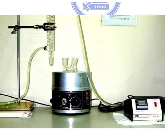
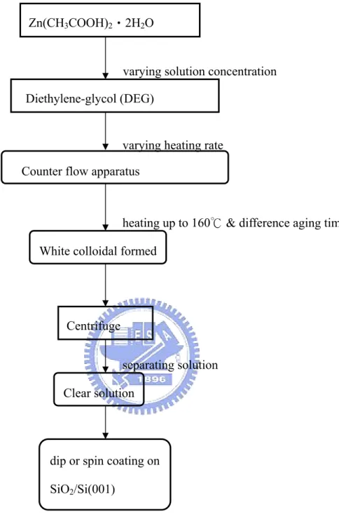
(29) Chapter 3 Experiment detail 3.1 Sample preparation We produce monodisperse ZnO colloidal spheres by sol-gel method.. Sol-gel method. was chosen due to its simple handling and narrow size distribution.. The ZnO. colloidal spheres were produced by a one-stage reaction process similar to that described by Seelig et al [33], and reactions were described as the following equations: ∆ Zn(CH 3COO) 2 + xH 2 O ⎯⎯→ Zn(OH − ) x (CH 3COO − ) 2− x + xCH 3COOH ,. (1). ∆ Zn(OH − ) x (CH 3COO − ) 2− x ⎯⎯→ ZnO + ( x − 1) H 2 O + (2 − x)CH 3COOH .. (2). Eq. (1) is the hydrolysis reaction for Zn(OAc)2 to form metal complexes.. We. increased the temperature of reflux from RT to 160oC and maintained for aging. The zinc complexes will dehydrate and remove acetic acid to form pure ZnO as Eq. (2) during the aging time.. Actually, the two reactions described above proceed. simultaneously while the temperature is over 110oC. All chemicals used in this study were reagent grade and employed without further purification. In a typical reaction, zinc acetate dihydrate (99.5% Zn(OAc)2, Riedel-deHaen) was added to diethylene glycol (99.5% DEG, EDTA). The first thing we notice is that we can control the quantum dots size with domination concentration of zinc acetate in the solvent (DEG).. This point will be examined later.. Then the temperature of. reaction solution was increased to 160℃ and maintained for different aging time. White colloidal ZnO was formed in the solution that was employed as the primary solution. Jezequel[34] et al., reported that this method produce monodisperse ZnO powders of various sizes with changing the heat rate of the reaction solution. A 20.
(30) primary reaction was performed as described above, and the product was placed in a centrifuge. The supernatant (DEG, dissolved reaction products, and unreacted ZnAc and water) was decanted off and saved, and the polydisperse powder was discarded. Finally, the supernatant was then dipped on substrates (SiO2/Si (001) or SiO2) and dried at 150℃.. 3.2 Microstructure and optical properties 3.2.1 X-ray diffraction The crystal structures of the as-grown powder were inspected by Bede D1 diffractometer at Industrial Technology Research Institute using a CuK X-ray source (λ=1.5405Å).. We used small angle diffraction.. The ω was fixed at 5 ∘ , the. scanning step was 0.04∘, scanning rate was 4 degree/min and count time was 1.00 second. Figure 3-2 shown XRD ω-2θ scans geometry. The dashed lines mean the trajectory of the incident beam and the detector to be in motion. The sizes of the nanocrystallites can be determined by X-ray diffraction using the measurement of the full width at half maximum (FWHM) of the X-ray diffraction lines. The average diameter is obtained by D =. 0.89λ , where D is the average B cos θ. diameter of the nanocrystallite, λ is the wavelength of the X-ray source, and B is the FWHM of X-ray diffraction peak at the diffraction angle θ.. 3.2.2 Optical absorption spectra Optical transmission or absorption measurements are routinely used by chemists to 21.
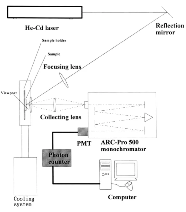
(31) determine the constituents of chemical compounds.. They are also used in the. semiconductor industry, but only for certain specialized applications.. We can. compute the band-gap of the semiconductors by the absorption spectra. The excitation and emission spectra were measured using U-4001 Spectrometer (Japan Spectroscopy) at Industrial Technology Research Institute with a lamp source of 150 W xenon.. Fist, we must find and take out background signal from. preparation sample.. Measurements were performed using a glass having a path. length of 2 mm. The intensity of emitted light was detected at a right angle to the incident light. Finally, we measured preparation sample (ZnO solution dip on SiO2 glass). Judging from the above, it can be concluded that background signal was deleted as we measure preparation sample. The measurement was taken in the range from 300 nm to 400 nm.. 3.2.3 Photoluminescence system Photoluminescence (PL) provides a non-destructive technique for the determination of certain impurities in semiconductors. The shallow-level and the deep-level of impurity states were detected by PL system. It was provided radiative recombination events dominate nonradiative recombination. In the PL measurements, the 325 nm line from a He–Cd laser was used as the excitation light. Light emission from the samples was collected into the TRIAX 320 spectrometer and detected by a photomultiplier tube (PMT). As shown in Fig. 3-3, the diagram of PL detection system includes mirror, focusing and collecting lens, the sample holder and the cooling system.. We utilized two single-grating. monochromators (TRIAX 320), one equipped with a CCD detector (CCD-3000), and the other equipped with a photo-multiplier tube (PMT-HVPS) and connected to a 22.
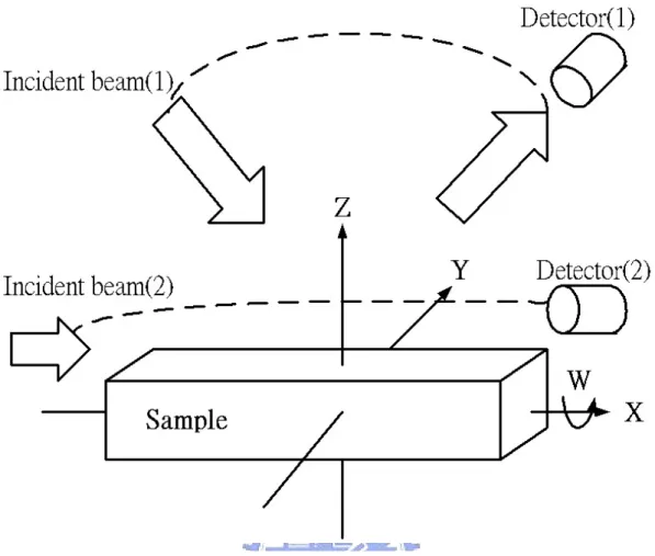
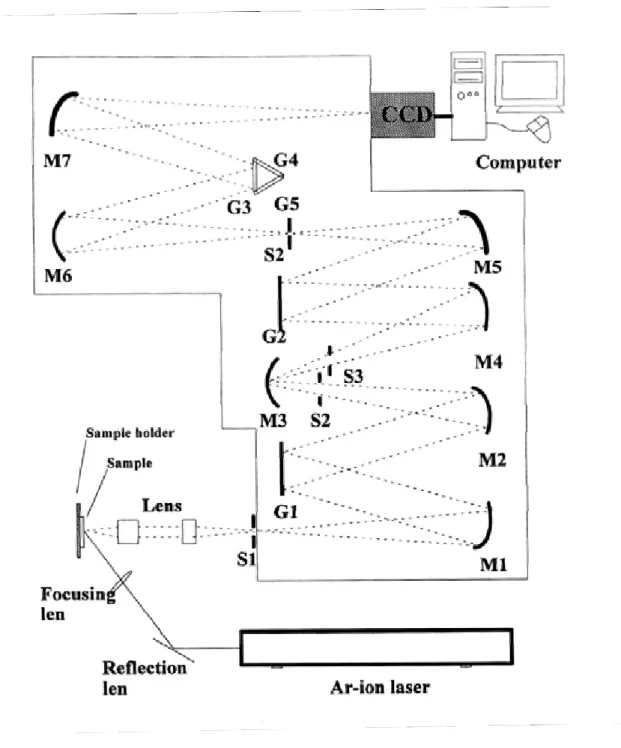
(32) photon counter for detection.. The normal applied voltage of PMT is 800 KV.. Moreover, we used a standard fluorescent lamps to calibrate our spectral response of spectrometer and detector. The PL signals are exposed about 0.1 sec at the step of 0.1 nm. The data are transmitted through a GPIB card and recorded by a computer. The monochromator (TRAIX 320) has a focal length of 32 cm with an optional side exit slit and has three selective 600, 1200 and 1800 grooves/mm gratings.. When the. entrance and exit slits are both opened to about 50 µm, the resolution is about 0.1 nm for the monochromator with PMT. The low-temperature PL measurements were carried out using a closed cycle cryogenic system.. 3.2.4 Raman system Raman scattering is a very powerful probe for investigating the vibration properties of materials. It is also influential in understanding problems as diverse as the structure of amorphous insulators, and the conduction mechanisms in ionic conductors. The experimental setup of Raman spectroscopy consists mainly of three components: a laser system serves as a powerful, monochromatic light source and a computer controlled spectrometer for wavelength analysis of the inelastically scattered light. Figure 3-4 show the experimental setup schematically. The Raman scattering was measured with an Ar-ion laser (Coherent INNOVA 90) as an excitation source emitting at a wavelength of 488 nm. The scattered light was collected by a camera lens and imaged onto the entrance slit of the Spex 1877C.. Light passes through the. entrance (S1) to be collimated by M1 onto G1 where it is dispersed onto M2. After passing through S2, which acts as the filter stage to determine the pass band, the light strikes the spatial-filter mirror (M3) and passes though a fixed slit, which eliminates much of the stray light. Again the light is collimated (M4), dispersed (G2), in an 23.
(33) opposing direction to cancel the effects of the initial dispersion, then focused (M5) onto the exit slit of the filter stage (S3) which controls the resolution of the next spectrograph stage.. In this final stage, the light is again collimated (M6) and. dispersed on whichever of the turreted gratings (G3, G4 and G5 as gratings of 600, 1200 and 1800 grooves/nm, respectively) is selected by the user. The camera mirror (M7) projects a flat image onto the focal plane where it is seen by CCD.. Chemical reagent. Molecular formula. Degree of Source purity. Zinc acetate dehydrate. Zn(CH3COOH)2‧2H2O. 99.5%. Riedel-deHaen. Diethylene glycol. C4H10O3. 99.5%. EDTA. Table 3.1. Shows that chemical reagent was used with sol-gel experiment. process.. Figure 3.1. Experiment equipment used for fabricating ZnO quantum dots (QDS).. 24.
(34) Zn(CH3COOH)2‧2H2O. varying solution concentration Diethylene-glycol (DEG). varying heating rate Counter flow apparatus. heating up to 160℃ & difference aging time White colloidal formed. Centrifuge separating solution Clear solution. dip or spin coating on SiO2/Si(001). Table 3.2. A flow chart of fabricate ZnO quantum dots (QDS) by sol-gel method.. 25.
(35) Figure 3-2 XRD ω-2θ scans geometry for ZnO nanoparticles.. 26.
(36) Figure 3-3 PL detection system.. 27.
(37) Figure 3-4 Raman detection system.. 28.
(38) Chapter 4 Results and discussion 4.1 HRTEM and X-ray diffraction measurement Shown in Fig. 4-1(a) is a typical high-resolution transmission electron microscope (HRTEM) image of the ZnO nanoparticles. Nanoparticles aged at 160 °C for 1 h and solution concentration of 0.06M was selected for particle size determination by HRTEM.. The particles shape are predominantly spherical, many also exhibit surface. facetting, as shown in the inset of Figure 4-1(a) where a step of one atomic layer can be seen. The nanoparticles are clearly well separated and essentially have some aggregation.. Figure 4-1(b) show the size distribution of particles after aging at. 160°C for 1 h (0.06M), obtained from analysis of more than 35 particles per sample. The average diameter of the number-weighted particles obtained from a colloid aged at 160°C for 1 h (0.06M) was determined to be 4.36 ± 0.3 nm. The XRD patterns of the prepared sample (ZnO solution dip on SiO2 glass) by the sol-gel process are shown in Figure 4-2. The diffraction lines are the powder X-ray diffraction pattern of the ZnO nanoparticles prepared in a different solution concentration. The diffraction pattern and interplane spacings can be well matched to the standard diffraction pattern of wurtzite ZnO, demonstrating the formation of wurtzite ZnO nanocrystals. All of the samples present similar XRD peaks that can be indexed as the wurtzite ZnO crystal structure with lattice constants a=3.253Å and c=5.219Å by Eq. 2-8, which are consistent with the value in the standard card (JCPDS 36-1451). No diffraction peaks of other species could be detected that indicates all 29.
(39) the precursors have been completely decomposed and no other crystal products were formed. It should be noted here that the full width at half maximum (FWHM) of the diffraction peaks increase with decreasing the concentration of zinc precursor duo to the size effect. The mean diameter of the ZnO nanocrystallites is evaluated from the FWHM of the (110) peak from 3.5nm to 12nm by Eq. 2-9 with the range of B from 0.75∘to 2.45∘, θ= 47.56∘and λ (wavelength of incident X-ray) is 1.5406Å. This value corresponds to the tail of the particle size distribution determined from HRTEM micrographs (Figure 4-2 (b)) and is close to the value of 4.2 nm obtained from the absorption data (see next section).. 4.2 Absorption and Photoluminescence Spectra Fig. 4-3 illustrates the room temperature optical absorption (dotted lines) and PL (solid line) spectra of different ZnO quantum dots with reacting solution concentration from 0.04M to 0.32M with aging 1h at 160 ℃ .. The. photoluminescence (PL) spectra of the six samples, which were excited with the laser of wavelength 325nm, are shown in Fig. 4-3 (solid line). An ultraviolet-blue (UV blue) emission occurs above the band gap energy of bulk ZnO (3.3 eV) and shifts to higher energies (3.3–3.435 eV) as the QD size decreases (12–3.5 nm). Since the Bohr diameter of the exciton in bulk ZnO is on the order of 2.34 nm, we must consider the electron hole Coulomb interaction in our samples and the particles are in the moderate to weak confinement regime. The absorption spectra are significantly blue-shifted compared to the bulk single crystal indicating that the particles are in the quantum regime. It can be clearly seen 30.
(40) that the growth of the particles depends on solution concentration. In addition, it can be seen that the spectral shift is retarded toward the end with decreasing solution concentration. These factors suggest that the solution concentration strongly affects the particle size and hence the optical properties. The absorption peaks for the six samples were then obtained as 3.437 eV [ Fig. 4-3(f)], 3.463 eV [Fig. 4-3(e)], 3.475 eV [Fig. 4-3(d)], 3.516 eV [Fig. 4-3(c)], 3.584 eV [Fig. 4-3(b)]and 3.67 eV [Fig. 4-3(a)], respectively. These values are all much larger than the absorption edge of the bulk ZnO (3.3 eV).. The average particle size as a function of solution. concentration was determined from the absorption spectra using the effective mass model derived by Brus [35-40]. In the weak-confinement regime, the confinement energy of the first excited electronic state can be approximated by Eq. 2-10 E1 S = E go − Ry * [1 −. µ πa B M. (. a. )2 ]. where E g 0 is the bulk band gap, Ry* is exciton binding energy, a is the particle radius, M is the total mass, and µ is the reduce mass. Figure 4-4 shows the bandgap versus particle diameter obtained from Eq. 2-10. The particle size was obtained from the band gap inferred from the optical absorption spectra taking E gbulk =3.4 eV, me*= 0.26, mh*= 0.59[41,42].. We also observed a size-dependent redshift of the PL. maximum relative to the absorption maximum.. This redshift increases as the. particle size decreases and has been observed in other II–VI nanocrystalline systems (e.g., CdSe, CdS). Our results suggest that size dependent phonon processes may be partly responsible. In this case, it gives an empirical relationship between the electron-phonon interaction and particle size.. The electron-phonon interaction. energy will be examined in the Raman spectra. Ultimately, however, the origin of the size-dependent redshifted emission remains unclear at present [43-47]. In additional, the PL spectra of different aging time (same solution concentration 31.
(41) 0.08M) are illustrated in Figure 4-6. Similar blue-shifted behaviors are also found as decreasing aging time.. As decreasing the aging time, the UV emission peak. undergoes a blue-shift from 3.336 eV to 3.37 eV with decreasing relative intensity. We attributed the phenomenon of blue-shift to quantum confinement effect. The PL spectra of different heating rate appear in Fig. 4-7.. The same phenomenon of. quantum confinement effect applies to different heating rate. We can safely say that the ZnO particles size can be controlled by reaction solution by varying concentration, aging time and heating rate.. 4.3 Raman spectra analysis Raman spectrum of the fine ZnO powder was shown in Table 4-1 [48], where the peaks at 331, 383, 438, 549, 584, and 660 cm-1 were clearly observed in the low wave-number region. The results of Raman spectra for ZnO quantum dots (QDs) with diameters of 4.4, 4.8, 5.9 and 6.4 nm are shown in Fig.4-8. Compared with its powder counterpart, several obvious changes could be observed. First, from the figure we can see that the Raman peaks around 520 and 620 cm-1 are not shifted in frequency. We attributed these peaks (520 and 620 cm-1) to signal of substrate [49]. On the other side, Raman peaks around 438 cm-1 (E2 mode) shifts toward lower frequency and their linewidths become larger with decreasing ZnO QDs diameter in the low wave-number region. Ultimately, the peak of longitudinal (LO) phonon was not observed. From the phenomenon was observed above, we will further examine it later on. It is well known that the phonon eigenstates in an ideal crystal are plane waves due to the infinite correlation length; therefore the k=0 momentum selection rule of the first order Raman spectrum can be satisfied. 32. When the crystalline is reduced to.
(42) the nanometer scale, the momentum selection rule will be relaxed. phonon with the wave vector k = k ′ ±. This allows the. 2π to participate in the first-order Raman L. scattering, where k ′ is the wave vector of the incident light and L is the size of the crystal. The phonon scattering will not be limited to the center of the Brillouin zone, and the phonon dispersion near the zone center must also be considered. As a result, the shift, broadening, and the asymmetry of the first order optical phonon can be observed. The modes originating from the photon scattering by first-, second-, and third-order LO phonons are clearly observed in the spectrum under resonant excitation by the 325 nm laser line (see Fig.4-9). The energy of this line is about 440 meV higher than the band gap of ZnO. It means that there is a case of incoming resonance, where the laser line is in resonance with an interband electronic transition. As one can see from Fig. 4-9, the intensity of the resonant Raman line were sharply and the intensity ratio (2LO/1LO) becomes weak by sizes of decreasing ZnO QOs.. Considering the. particle size dispersion and assuming for R a Gaussian distribution f(R), the total Raman cross section for an n-phonon process can be written as[50, 51]. σ n = ∫ σ nR (ω ) f ( R)dR, σ (ω ) = µ R n. 4. nm m0. ∞. ∑E. m =0. 0. + nhω LO − hω + ihΓ. 2. ,. where µ is the electronic dipole transition moment, E0 is the (size-dependent) energy of the electronic transition, hω and hω LO are the energies of the incident photon and the LO phonon, respectively, m denotes the intermediate vibrational level in the excited state, and Γ is the homogeneous linewidth. The overlap integral between the ground and excited states wave functions can be written as [50, 51]. 33.
(43) 1. − ∆ (n−m) n−m ⎛ n! ⎞ 2 n m = ⎜ ⎟ exp( )∆ Lm ( ∆ ) 2 , m ! 2 ⎝ ⎠ 2. where Lnm−m denotes a Laguerre polynomial and ∆ is the dimensionless displacement of the harmonic oscillator in the excited state. ∆ is known to be related to the Huang-Rhys parameter S by the relation S=∆2.. Therefore, the ratio σ between. two-phonon and one-phonon scattering cross sections is a very sensitive function of the electron-phonon coupling strength. However, σ is strongly dependence of the excitation photon energy and E0 is the (size-dependent) energy of the electronic transition.. Nevertheless, we observed the lower intensity ratio (I2LO/I1LO) as. decreasing the size of ZnO QDs. Let us move to the origin of electron-phonon coupling in ZnO QDs.. It is. generally accepted that the electron phonon coupling is governed by two mechanisms: the deformation potential and the Frohlich potential. Following Loudon[52] and Kaminow and Johnston[53], the TO Raman scattering cross section is mainly determined by the deformation potential that involves the short-range interaction between the lattice displacement and the electrons.. On the other hand, the LO. Raman scattering cross section includes contributions from both the Frohlich potential that involves the long-range interaction generated by the macroscopic electric field associated with the LO phonons and the deformation potential. We found that the intensity of TO phonon in ZnO QDS is almost insensitive to the incident laser wavelength, while that of E1 (LO) phonon is greatly enhanced under the resonant conditions. Therefore we believe that the electron-LO interaction at decreasing the nanocrystal size is mainly associated with the Frohlich interaction.. 34.
(44) (a) 70 60. Fequency(%). 50 40 30 20 10 0 2.5. 3.0. 3.5. 4.0. 4.5. 5.0. 5.5. Particles radius(nm). (b). Fig. 4-1 HRTEM image (a) and size distribution (b) of the ZnO QDs fabricated using 0.06M Zn(OAc)2.. 35.
(45) (101) solution concentration: (a)0.04M(b)0.06M (100) (c)0.08M(d)0.1M(e)0.16M(f)0.32M (002). XRD Intensity (a. u.). (102). (110) (103) (112) (f)12nm (e)7.4nm (d)6.5nm (c)5.3nm (b)4.2nm (a)3.5nm. 30. 40. 50. 60. 70. Two Theta (degree). Fig. 4-2 XRD profiles of the ZnO QDs prepared with various concentration of Zn(OAc)2.. 36.
(46) 1.2. 12 nm. 0.6 0.0. 7.4 nm. 0.6 0.0 1.2 0.6. 6.5 nm. 0.0 1.2. 5.3 nm. 0.6 0.0. Absorption (arb. units). PL Intensity (arb. units). 1.2. 1.2. 4.2 nm. 0.6 0.0 1.2 0.6. 3.5 nm. 0.0. 2.8. 3.2. 3.6. 4.0. Photon Energy (eV). Fig. 4-3 PL (solid line) and absorption (dashed line) spectra near the band edge of various ZnO QD size.. 37.
(47) Photon energy(eV). 3.7 3.6 3.5 3.4 a B =2.34nm. 3.3. 2. 4. 6. 8. 10. 12. 14. Particle size(nm). Binding energy(meV). (a). 120. 80 Bulk binding energy. 40 20 Particle size(nm). 40. (b) Fig. 4-4 The dependence of the band gap enlargement (a) and exciton binding energy (b) versus the ZnO QDs diameter as calculated from the effective mass model and the corresponding experimental data. 38.
(48) 0.24. Stokes shift(eV). 0.22 0.20 0.18 0.16 0.14 2. 4. 6. 8. 10. 12. 14. Particle size(nm). Fig. 4-5 The dependence of the Stokes shift versus the ZnO QDs diameter.. 39.
(49) Intensity(a.u.). Difference aging time at solution concentration 0.8M : (a)0.5h (b)1h (c)1.5h (d) 2h (d). (c) (b) (a). 2.0. 2.2. 2.4. 2.6. 2.8. 3.0. 3.2. 3.4. 3.6. Photon energy(eV). Fig. 4-6 PL spectra of various aging time at 0.08M solution concentration.. variation heating rate: (a)1C/m (b)3C/m (c)5C/m (d)7C/m. (d). Intensity(a.u.). (c). (b) (a). 2.2. 2.4. 2.6 2.8 3.0 3.2 Phonton energy(eV). 3.4. 3.6. Fig. 4-7 PL spectra of various heating rate at 0.1M solution concentration.. 40.
(50) Wave number(cm-1). Symmetry. Process. 331. A1. Acoust. Overton. 383. A1(TO). First process. 410. E1(TO). First process. 438. E2. First process. 540. A1(LO). First process. 584. E1(LO). First process. 660. A1. Acoust. Overton. 776. A1,E2. Acoust. Opt. comb.. Table 4-1 The Raman spectral peaks of the fine ZnO powder.. 41.
(51) Ranman of variation solution concentration: (a)0.1M (b)0.08M (c)0.07M (d)0.06M. Intensity(a.u.). (d)4.4nm. (c)4.8nm. (b)5.9nm. (a)6.4nm. 400. 500 -1 Raman shift (cm ). 600. 700. 28. 439. 26 24 22 437. 20 18. 436. 16 14. 435. 12 434 4.0. 4.5. 5.0. 5.5. 6.0. 6.5. Particle size (nm). Fig. 4-8 Raman spectra of various ZnO QD.. 42. 10 7.0. FWHM (cm-1). Raman shift (cm-1). 438.
(52) Intensity(a.u.). 1LO. 2LO 3LO (a)4.4nm (b)4.9nm (c)5.9nm (d)6.5nm (e)20nm. 600. 800. 1000 1200 1400 1600 -1 Raman shift(cm ). 1800. 2000. 3.5 J. Phys. D 34, 3430 (2001). 3.0. I2LO/I1LO. 2.5 2.0 1.5 1.0 0.5 0.0 0. 5. 10. 15. 20. 25. 30. diameter of ZnO crystal (nm). Fig. 4-9 Resonant Raman Spectra of various ZnO QD.. 43. 35.
(53) Chapter 5 Conclusion and perspectives 5.1 Conclusion Stable ZnO nanoparticles with 3.5-12 nm in diameter were made by a rapid and continuous process of sol-gel method.. The ZnO nanoparticles show a wurzite. structure with variation of diameter of ZnO nanoparticles from 3.5 nm to 12 nm by x-ray diffraction. These particles exhibit quantum size effect (blue-shift of the absorption and PL spectrum with decreasing crystallite size) and nicely followed a correlation between particle size and optical energy gap from the effective mass model of ZnO quantum dots. Furthermore, we have measured Raman spectra of ZnO quantum dots with different diameters.. The shift, broadening, and the. asymmetry of the optical phonons have been found for ZnO quantum dots compared with ZnO bulk. The phonon confinement effect could account for these observed results. Moreover, we have extracted the electron-phonon-coupling parameter from Raman spectra, and unambiguously demonstrate that electron-phonon-coupling increase with increasing nanocrystal size mainly due to the Frohlich interaction.. 5.2 Perspectives In the process of fabricating the ZnO quantum dots by sol-gel, the smaller size and uniform distribution nanoparticles are our major targets.. To achieve better. homogeneity of sample, we should upgrade the centrifugal technique and the method of chemical synthesis. For optical properties, the emission characteristic of ZnO quantum dot is going to measure by low temperature photoluminescence spectra. 44.
(54) The most important characteristic of the ZnO QDs is the exciton lifetime, and we will use the pump-probe experiment to analyze it.. 45.
(55) References 1.. 2. 3.. 4. 5. 6. 7.. 8. 9. 10. 11. 12.. 13.. 14.. 15.. 16. 17. 18. 19.. 20.. 21. 22.. 23. 24. 25.. Heath, J. R., Ed. Acc. Chem. Res. 1999, Special Issue for Nanostructures, review articles relevant to colloidal nanocrystals. A. P. Alivisatos, Science 271, 933 (1996). F. C. Lin, Y. Takao, Y. Shimizu, and M. Egashira, Sens. Actuators B 24-25, 843 (1995). K. S. Weissenrieder and J. Muller, Thin Solid Films, 30, 300 (1997). J. Muller and S. Weissenrieder, J. Anal. Chem. 349, 380 (1994). S. C Minne, S. R. Manalis, and C. F. Quate, Appl. Phys. Lett. 67, 3918 (1995). Karin Keis, Nanostructured ZnO Electrodes for Solar Cell Applications, (Acta Universitatis Upsaliensis, Uppsala, 2001). J. B. Baxter, and E. S. Aydil, Appl. Phys. Lett. 86, 053114 (2005). R. L. Hoffman, B. J. Norris, and J. F. Wager, Appl. Phys. Lett. 82, 733 (2003). W. I. Park and G. C. Yi, Adv. Mater. 16, 1907 (2003). R. Könenkamp, R. C. Word, and C. Schlegel, Appl. Phys. Lett. 85, 6004 (2004). Z. K. Tang, G. K. L. Wong, P. Yu, M. Kawasaki, A. Ohtomo, H. Koinuma, and Y. Segawa, Appl. Phys. Lett. 72, 3270 (1998). T. Makino, C. Chia, Y. Segawa, M. Kawasaki, A. Ohtomo, K. Tamura, Y. Matsumoto, and H. Koinuma, Appl. Surf. Sci. 189, 277 (2002). D. W. Bahnemann, C. Kormann, and M. R. Hoffmann, J. Phys. Chem. 91, 3789 (1987). L. Guo, S. Yang, C. Yang, P. Yu, J. Wang, W. Ge, G. K. L. Wong, Appl. Phys. Lett. 76, 2901 (2000). E. A. Meulenkamp, J. Phys. Chem. B 102, 5566 (1998). E. M. Wong, J. E. Bonevich, P. C. Searson, J. Phys. Chem. B 102, 7770 (1998). S. Sakohara, M. Ishida, M. A. Anderson J. Phys. Chem. B 102, 10169 (1998). S. Mahamuni, K. Borgohain, B. S. Bendre, V. J. Leppert, S. H. Risbud, J. Appl. Phys. 85, 2861 (1999). H. Zhou, H. Alves, D. M. Hofmann, W. Kriegseis, B. K. Meyer, G. Kaczmarczyk, A. Hoffmann, Appl. Phys. Lett. 80, 210 (2002). E. M. Wong, P. C. Searson, Appl. Phys. Lett. 74, 2939 (1999). A. Germeau, A. L. Roest, D. Vanmaekelbergh, G. Allan, C. Delerue, E. A. Meulenkamp, Phys. Rev. Lett. 90, 097401 (2003). V. A. Fonoberov, A. A. Balandin, Appl. Phys. Lett. 85, 5971 (2004). C. J. Brinker and G. W. Scherer, “Sol-Gel Sience”, p. 303. C. F. Klingshirn, “Semiconductor Optics”,p.169. (1997). 46.
(56) 26.. 27.. 28.. 29.. 30.. Sun-Bin Yin, “Fabrication and Characterization of CdS and ZnSe Microcrystalline Doped Glass Thin Films by Pulsed Laser Deposition”, p.7. National Chiao Tung University Department of Photonics, (1999). Jasprit Singh, “Physics of Semiconductors and Their Heterostructures”, p.17 (1993). Yi-Chin Lee, “Effect of Biaxial Stress on ZnO Thin Films and in-Plane Optical Gain”, p.11. National Chiao Tung University Department of Photonics, (2004). Sun-Bin Yin, “Fabrication and Characterization of CdS and ZnSe Microcrystalline Doped Glass Thin Films by Pulsed Laser Deposition”, p.13. National Chiao Tung University Department of Photonics, (1999). A. Taylor, “X-ray Metallography”(John Wiley and Sons, New York), p.676 (1961).. 31. 32. 33.. 34.. 35. 36. 37. 38. 39. 40. 41.. 42. 43. 44.. 45. 46.. 47.. 48. 49.. C. F. Klingshirn, “Semiconductor Optics”,p.162 (1997). *Jasprit Singh, “Physics of Semiconductors and Their Heterostructures”, p. 316. E. W. Seelig, B. Tang, A. Yamilov, H. Cao, and R.P.H. Chang, Mater. Chem Phys. 80, 257 (2003). D. Jezequel, J. Guenot, N. Jouini, F. Fievet, Mater. Sci. Forum 152–153 (1994) 339. Brus, L. E. J. Chem. Phys. 79 (11), 5566-5671 (1983). Brus, L. E. J. Chem. Phys. 80 (9), 4403-4409 (1984). Brus, L. E. Nanostruct. Mater.,1, 71-75 (1992). Steigerwald, M. L.; Brus, L. E. Acc. Chem. Res. 23, 183-188 (1990). Wilson, W. L.; Szajowski, P. F.; Brus, L. E. Science. 262, 1242-1244 (1993). Ramaniah, L. M.; Nair, S. V. Physica B. 212, 245-250 (1995). S. Shionoya, in Phosphor Handbook (Eds: S. Shionoya, W. M. Yen), CRC, Boca Raton, FL (1998). L. I. Berger, Semiconductor Materials, CRC, Boca Raton, FL (1997). H. Fu and A. Zunger, Phys. Rev. B 56, 1496 (1997). L. Banyai and S. W. Koch, Semiconductor Quantum Dots, Series onAtomic, Molecular, and Optical Physics (World Scientific, Singapore,1993), Vol. 2. H. Fu and A. Zunger, Phys. Rev. B 55, 1642 (1997). M. Nirmal, D. J. Norris, M. Kuno, M. G. Bawendi, Al. L. Efros, and M. Rosen, Phys. Rev. Lett. 75, 3728 (1995). C. A. Smith, H. W. H. Lee, V. J. Leppert, and S. H. Risbud, Appl. Phys. Lett. 75, 1688 (1999). R. P. Wang, G. Xu and P. Jin, Phys. Rev. B 69, 113303 (2004). Rong-ping Wang, Guang-wen Zhou, Yu-long Liu, Shao-hua Pan, Hong-zhou 47.
(57) 50.. 51.. 52. 53.. Zhang and Da-peng Yu, Phys. Rev. B 61, 16 827 (2000). A. P. Alivisatos, T. D. Harris, P. T. Carrol, M. L. Steigerwald, and L. E. Brus, J. Chem. Phys. 90, 3463 (1990). G. Scamarcio,* V. Spagnolo, G. Ventruti, M. Lugara´ and G. C. Righini, Phys. Rev. B 53, 10 489 (1996). R. Loudon, Adv. Phys. 13, 23 (1964). I.P. Kaminow and W.D. Johnston, Phys. Rev. 160, 19 (1967).. 48.
(58)
數據
+7
相關文件
The formation mechanism has been studied in this work through dynamic light scattering method which can get information about growth and distribution curve of particle size in
In the size estimate problem studied in [FLVW], the essential tool is a three-region inequality which is obtained by applying the Carleman estimate for the second order
He proposed a fixed point algorithm and a gradient projection method with constant step size based on the dual formulation of total variation.. These two algorithms soon became
Project 1.3 Use parametric bootstrap and nonparametric bootstrap to approximate the dis- tribution of median based on a data with sam- ple size 20 from a standard normal
In the inverse boundary value problems of isotropic elasticity and complex conductivity, we derive estimates for the volume fraction of an inclusion whose physical parameters
Al atoms are larger than N atoms because as you trace the path between N and Al on the periodic table, you move down a column (atomic size increases) and then to the left across
Two examples of the randomly generated EoSs (dashed lines) and the machine learning outputs (solid lines) reconstructed from 15 data points.. size 100) and 1 (with the batch size 10)
The closing inventory value calculated under the Absorption Costing method is higher than Marginal Costing, as fixed production costs are treated as product and costs will be carried
