國 立 交 通 大 學
電 機 與 控 制 工 程 研 究 所
碩 士 論 文
超低功率溫度感測器前端電路
An Ultra Low-Power Front-end Circuit for
Temperature Sensor
研 究 生:吳宗諭
指導教授:蘇朝琴 教授
An Ultra Low-Power Front-end Circuit for
Temperature Sensor
研 究 生:吳宗諭 Student
:
Tsung-Yu
wu
指導教授:蘇朝琴 教授
Advisor : Chau-Chin Su
國 立 交 通 大 學
電 機 與 控 制 工 程 研 究 所
碩 士 論 文
A ThesisSubmitted to Department of Computer and Information Science College of Electrical Engineering and Computer Science
National Chiao Tung University In partial Fulfillment of the Requirements
for the Degree of Master
in
Electrical and Control Engineering October 2006
Hsinchu, Taiwan, Republic of China
研究生:吳宗諭 指導教授:蘇朝琴
國立交通大學電機與控制工程研究所
摘要
近年來,感測器在 IC 市場上有所進步。在一般的積體電路製程中結合感測 器為顯著的趨勢。因此,結合電路與感測器不僅僅能降低電路的複雜度更能因此 降低成本上的支出。另外,低功率低電壓更是未來的另一個趨勢。如何節省功率 的消耗將是一大問題。 在此論文中,提出一個應用於低功率與低電壓的溫度感測器前端電路。為了 達到低功率與低電壓,操做在弱反轉區的放大器將會被介紹。在這前端電路中, 由於溫度感測器的訊號相當小,截波放大器(chopper amplifier)將在論文中被使 用。除此之外,非連續性的低通濾波器也會被介紹。為了降低製程偏移的影響, 使用一些電路技巧,用以消除運算放大器的偏移電壓。由於電路中使用到時脈開 關,雜訊應此將會產生。因此在論文中藉由多餘的開關(dummy switches)製造反 相的雜訊以消除單一開關所產生之雜訊。 在論文中,溫度感測器前端電路在 TSMC CMOS 0.18 Mμ 的製程被實現。此 前端電路包括截波放大器、濾波器、後端放大器。其晶片面積為 0.78 mμ X 0.78μm(不包含 PAD)。取樣頻率在 6.4k,整體功率為 5.6μW,訊號頻率為 50Hz。 索引詞彙—截波放大器、電容切換式低通率、低電壓、低功率、反相器、偏移電 壓消除。Temperature Sensor
Student: Tsung-Yu wu Advisor: Chau-Chin Su
Institute of Electrical and Control Engineering
Nation Chiao Tung University
Abstract
Sensors advanced greatly in the field of semiconductor in recent years. A notable trend is to realize a sensor in a standard CMOS processing. A combination of micro-sensor and circuits decrease the complexity of package and make cost down. On the other hand, low-voltage low-power techniques are necessary to increase the battery life time in the future. How to decrease the power consumption is a serious problem in our design.
In this thesis, a low-power low-voltage front-end circuit of the thermopile is implemented. The amplifier working in weak inversion is introduced in order to reduce the power consumption. Because the output signal of the thermopile is very small, a chopper amplifier is needed in the front-end circuits to improve the SNR. Also, a switch-capacitor lowpass filter will be implemented following the chopper amplifier. To reduce the effects of process variation of amplifiers, a offset-cancellation technique is introduced. Dummy switches are used to reduce the clock feedthrough noise in our design.
In this thesis, the front-end circuit is realized with TSMC CMOS 0.18μm. It includes chopper amplifier, filter, and post amplifier. The core area is 0.78μmX
0.78μm. The clock is 6.4k Hz, the power is 5.6μW , the signal bandwidth is 50 Hz.
Index Terms – chopper amplifier, switched-capacitor circuits, low-voltage, low-power, offset cancellation
在此要感謝我的父母,讓我無後顧之憂的完成學業。還有感謝父母在我最失 意最灰暗的時候,給我鼓勵讓我能夠安下心繼續努力。不管是在學業上或是其它 方面更能專注的學習。 特別要感謝的是我的指導老師 蘇朝琴 教授,讓當初沒有專業知識的我進 入實驗室學習。兩年中,讓我深深的反省自己讓我更了解自己。除此之外,老師 的人生體悟,讓我不只在專業上更在待人處事上能有深切的認知。經過兩年的訓 練,讓我在困難中不至於亂了方寸,能更有勇氣的走下去。 在此還要感謝一起在實驗室的學長、同學、學弟及助理們。很謝謝楙軒、匡 良讓我看到做事的拼勁、專注,以及待人接物上該有的態度。感謝小冠讓我體會 到面對困境該保有的幽默。特別要感謝智琦,在最困難的時候伸出援手,更讓我 看到面對困境該有的心態,以及作研究精神、更重要的是對人的謙遜,不急躁不 冒進以及目標的確定與實行。丸子、鴻文、仁乾、盈杰學長们對事情追根究底的 態度以及對自己理想以及興趣付出的神情。以及柏成、瑛佑、阿達、ku、阿銘學 長们的指導,還有順閔、祥哥、教主、snoopy、忠傑、方董、小馬、賢哥、村鑫、 存遠大家面對人生的選擇、態度都讓我獲益良多。讓我這兩年來,過的相當充實, 也學到很多。 吳宗諭 20060802
Abstract ... ii
Table of Contents ... iv
Lists of Figures ... vi
Lists of Tables ... viii
Chapter 1 Introduction ...1
1.1 Motivation...1
1.2 Basic Concepts of Thermopile...2
1.3 Thesis Organization ...3
Chapter 2 Noise and Dynamic Offset Cancellation Technology Analysis
...4
2.1 Introduction...4
2.2 Type of Noise ...4
2.3 Autozero Technigue ...7
2.4 The Chopper Stabilization Technique ...9
2.5 Summary ...16
Chapter 3 Design Considerations for Low-Voltage Low-Power Chopper
Amplifier...17
3.1 Introduction...17
3.2 Weak Inversion in the MOS Transistor...17
3.3 Filter in Chopper Amplifier ...21
3.4 Low-Voltage Switch...29
3.5 Summary ...31
Chapter 4 The Front-end Circuit of the Thermopile ...32
4.1 Introduction...32
4.2 System Architecture ...32
4.3 Implementation of Chopper Amplifier...34
4.4 Filter Design...41
4.5 Post Amplifier ...46
4.6 Clock Generator ...47
4.7 Simulation Result and Circuit...48
Chapter 5 Conclusions ...54
Figure 1.1 The see-back effect ...3
Figure 2.1 (a) Thermal noise in resistor , (b) Power spectrum density...5
Figure 2.3 The production of the flicker noise ...6
Figure 2.4 Noise spectrum of noise ...7
Figure 2.5 Principle of autozero technique ...8
Figure 2.6 Noise power spectrum of autozero ...8
Figure 2.7 The integrator with CDS (a) architecture, (b) during φ1, (c) during φ2 ...9
Figure 2.8 The principle of the chopper technique ...10
Figure 2.9 The principle of chopper in time domain ... 11
Figure 2.10 The principle in the time domain... 11
Figure 2.11 Chopper modulation ...12
Figure 2.12 The architecture of the chopper ...13
Figure 2.13 The circuit of the modulation signal...13
Figure 2.14 The spectrum after filter ...13
Figure 2.15 Clock feedthrough ...14
Figure 2.16 Channel charge injection ...15
Figure 2.17 Spike signal of the switch...15
Figure 2.18 The dummy switch ...15
Figure 2.19 The NMOS chopper realization...16
Figure 3.1 MOS weak inversion characteristics ...19
Figure 3.2 Transconductance to current ratio versus overdrive ...20
Figure 3.3 Drain current versus drain-source voltage in weak inversion ...20
Figure 3.4 Resistor equivalence of the switched-capacitor ...21
Figure 3.5 Parasitic-insensitive integrator ...22
Figure 3.6 The parasitic-sensitive integrator ...23
Figure 3.7 A non-inverting delaying integrator...24
Figure 3.8 Behavior in each clock (a)φ1 (b)φ2...24
Figure 3.9 Delay-free integrator ...25
Figure 3.10 A first-order active-RC filter ...25
Figure 3.11 Discrete-time form...26
Figure 3.12 The block diagram of the biquad filter ...27
Figure 3.15 High-Q switched-capacitor biquad filter ...28
Figure 3.16 Transmission gate conductance at (a) standard, (b)low supply voltage ...29
Figure 3.17 Voltage boosted clock driver ...30
Figure 3.18 Voltage doubler...31
Figure 4.1 Block diagram of the temperature sensor...33
Figure 4.2 Noise model...34
Figure 4.3 Noise analysis...35
Figure4. 4 Noise analysis in telescopic current ...37
Figure 4.5 The design flow ...40
Figure 4.6 The Bode Diagram ...41
Figure 4.7 Noise model during φ1...42
Figure 4.8 (a) amplifier small-signal, (b) noise model in φ2...43
Figure 4.9 The architecture of the low pass filter ...44
Figure 4.10 (a) the linearity circuit, (b) transconductance...45
Figure 4.11 The improvement gain circuit...46
Figure 4.12 The post amplifier...46
Figure 4.13 Behavior (a) φ1 ,(b) φ2...47
Figure 4.22 The clock generator ...48
Figure 4.23 Bias circuit...48
Figure 4.24 The chopper amplifier ...49
Figure 4.25 CMFB circuit...49
Figure 4.26 The current mirror amplifier...50
Figure 4.27 The front-end circuit of the thermopile sensor ...51
Figure 4.28 The signal output (a) the chopper amplifier, (b) filter ,(c)post-amplifier .52 Figure 4.29 The layout of the front-end circuit for temperature sensor...53
Table 1 The gain of the block...38
Table 2 Current mirror type ...40
Table 3 The telescopic amplifier type ...41
Table 4 The parameter of the switched capacitor filter...42
Table 6 The specification of the chopper amplifier ...52
Table 7 The efficient factor for the front-end circuit ...55
Chapter 1
Introduction
1.1 Motivation
In recent years, IC processing technologies have a great improvement. It not only increases the performance but also scales down the price. In the intelligent sensor, how to scale down the price is important. Therefore, the sensor using standard (CMOS) technology is cheaper than previous system solution. Another advantage in sensor using standard technology is that it can combine with the circuit. The circuit for signal processing, A/D conversion, on-chip calibration can increase the performance in the smart sensor. Therefore, integrating the micro-sensor and circuit is a trend to scale down the price and increase the performance.
The temperature sensor is an important device in smart sensor market. The applications of sensors have many aspects, like ear thermometer and home climate control. Ear thermometers, the temperature measurement are widely used in hospital, Fast and accuracy are the important point. The home climate control is similar to the ear thermometer. It is important to check the temperature in the room then to enhance the comfort level of the room. The thermopile is one of the temperature sensors. The
thermopile can transfer temperature to the heat then transfer the heat to the voltage. Because the voltage from the thermopile is too small, the thermopile sensor is limited by the offset and noise of the input of the amplifier. Therefore, to remove noise and offset voltage is a main subject. The solutions that can remove offset voltage and low frequency noise are invented. Examples of these are the autozero and chopper technology. The principle of the autozero technique is that the offset cancellation is done in two phase [1]. The principle of the chopper technique is to move the offset voltage to a high frequency and modulate back to the base-band. The offset is only modulated once, so the higher frequency needs to be canceled. Therefore the low frequency noise can be cancelled and the input signal is maintained. The signal noise ratio (SNR) is improved.
In this thesis, the low-voltage, low-power front-end circuit of the thermopile is present. Using the amplifier which works in weak inversion enables the front-end circuits to achieve tens of micro voltage. How to cancel the offset and low frequency noise is included in it.
1.2 Basic
Concepts
of
Thermopile
In recent years, the thermopile techniques are developed and commercialized [26]. The well-known product is the infrared temperature sensor which use in the ear thermometer. Aside from the ear thermometer and pyrometer, the new application that includes the automated climate control and other housed held such as microwave ovens and hair dryers are invented.
In this thesis, the thermopile sensor is introduced. The thermopile is a popular device using the concept of the see-back effect. The principle of the see-back effect is shown in Figure1.1.The mate. A, B, and C have different thermoelectric factorαA ,αB,and αc. The junctions of the metal A and B are at higher temperature
h
T (hot point) and the metal C is at lower temperature T (cool point). Therefore, the C differential voltage is produced. The voltage across A and B is proportional to temperature difference and the metal A and B.
(
)
(
)
AB A B h C
V = α −α T −T (1-1)
At thermoelectric sensor consists of several thermocouples connects in series that form a thermopile. In recent years, the thermopile sensors use the silicon and metal as
the thermoelectric material.
According to differential metals, the voltage can be produced. The equation in semiconductor is:
a V T α
Δ = Δ ⋅ (1-2)
where the αa is the see-back coefficient for material and Δ is the temperature T difference between the end of the conductor. According to the principle, the temperature sensor can be design.
Figure 1.1 The see-back effect
1.3 Thesis
Organization
This thesis is organized into five chapters. In Chapter 1, this thesis and the thermopile are briefly introduced. In Chapter 2, the basic concepts of chopper, the MOS working in the weak inversion, and the noise autozero technique are introduced.
In Chapter 3, the noises of the amplifier, and design amplifier, filter architecture and clock generator are outlined. In Chapter 4, the total architecture of the thermopile is presented. The pre-amp, filter and the post-amp are include it. In Chapter 5, the front-end circuits are mentioned and compared.
h T MetalB MetalA MetalC MetalC c T AB V + -c T
Chapter 2
Noise and Dynamic Offset
Cancellation Technology Analysis
2.1 Introduction
Some of the fundamental issues in the design of amplifier will be reviewed in this chapter. Input signal is influenced by the noise produced by the amplifier. The discussion of the noise source is presented in the Section 2.1. Next, in Section 2.2 to 2.4, the dynamic offset cancellation technologies is introduced. Section 2.2 present the technology named Autozero (AZ) [1]. In Section 2.3 and 2.4, there are two basic techniques that are used to reduce the offset and low frequency of amplifier. Section The Correlation Double Sampling (CDS) is introduced in Section 2.3. Chopper Stabilization (CHS) is introduced in Section 2.4.
2.2
Type of Noise
There are two basic noise sources from the analog circuits. The noises are produced by the electronic device. First, the major source of noise in the resistor is thermal noise. It appears as white noise and can be model as an independent voltage
source. Second, another noise source is flicker noise (1/f noise) [23]. Unlike thermal noise, it just only appears in the low frequency.
2.2.1 Thermal
Noise
The thermal noise is the random motion of the electrons in a conductor. Therefore, there is some fluctuation in the voltage measurement even if there is not any voltage source.
The thermal noise in the spectrum is white. It distribute uniformly in the frequency spectrum. Like the thermal noise of a resistor R, it is module as voltage source, shown in Figure 2.1
Figure 2.1 (a) Thermal noise in resistor , (b) Power spectrum density The thermal noise of a resistors R with the one-side spectral density is
( ) 4 , Sv f = KTR f≥0. (2-1) Where k= 23 10 38 .
1 × − J/k is the Boltzmann constant, T is the absolute temperature, and the R is the resistance of the resistor.
In MOSFET, MOS also exhibits the thermal noise. Normally, the thermal noise of the MOS is model by a current source. Its spectral density is:
2 4
In = KTgmγ . (2-2)
Like Fig 2.2. The coefficient γ is derived as 2/3, therefore the spectral density can be written as 2 4 2 3 In = KT gm. f ) ( f SV 2 Vn R 4KTR Noiseless Resister
2.2.2 Flicker
Noise
Some noises appear in the low frequency is called flicker noise [23]. The reason of the flicker noise is that when silicon crystal reaches the interface, many dandling bonds appear. It takes extra energy and later releases energy. This phenomenon introduces the flicker noise as shown in Figure 2.3. Simultaneously, the flicker noise is also called 1/f noise.
Figure 2.3 The production of the flicker noise
Unlike thermal noise, the flicker noise is not white. The energy of the flicker noise is concentrated at the low frequency. Its spectral density is:
f WL C K V ox f n 1 2 ⋅ = (2-3)
where Kf is the fabrication parameter, Coxis the gate capacitor per unit area, and W and L are the size of the MOS. The spectral density of the flicker noise is shown in Figure 2.4 and the thermal noise is included [2]. The magnitude of the flicker noise is inversely proportional to the frequency.
Polysilicon Silicon Crystal 2 SiO Dangling Bonds gm KT In 4 γ 2
Figure 2.4 Noise spectrum of noise
In Fig 2.4 the intersection between flicker noise and thermal noise is called flicker noise frequency.
2.3 Autozero
Technigue
The autozero technique (AZ) [2] is a method of offset voltage cancellations. It can improve the SNR of the system. The correlated double sampling is similar to autozero technique. Next, in Section 2.3.1, the AZ is presented. Then, in Section 2.3.2 the correlated double sampling is outlined latter.
An autozeroing amplifier is shown in Figure 2.5. The principle of autozero technique is to cancel offset voltage in two phases. In first phase φ1, input voltage is set zero, then let offset voltage be sampled on C . In second phaseaz φ2, when input signal enter to the amplifier, the offset sampling on C is subtracted than amplified. az Through this way, the offset voltage can be cancelled. In the meantime, the low frequency noise is also cancelled. Because, when noise is in low frequency, the characteristic of it belong to DC. So low frequency noise can be regard as DC offset.
In order to remove low frequency and offset voltage, sampling frequency ( f ) s must higher than 1/f noise corner frequency. So the noise lower than f can be s stored on the C , it will be cancelled in the next phase. However, the noise comes az form switched is also sampled on theC . Therefore, the noise lower than az f folded s back to increase the noise level. Therefore, the noise level must be higher than thermal noise as shown in figure 2.6.
Flicker noise Thermal noise )) / (log(V Hz Vn f
Figure 2.5 Principle of autozero technique
Figure 2.6 Noise power spectrum of autozero
2.3.2 Correlation Double Sampling
The correlation double sampling technique (CDS) [1] is regarded as a special case of the AZ (autozero). As its name indicates, the offset voltage and low frequency noise are sampled at each phase.
In AZ, there are two phases to remove offset voltage. The first one is used to sample the low frequency noise and offset voltage, the second one is used to cancel the offset voltage and amplify the input signal. Therefore, the AZ phase may require one additional phase. The characterization of the CDS like AZ is suitable for SC (switched capacitor) circuit.
Figure 2.7 shows the architecture of the integrator with double sampling. When 1 φ 1 φ 2 φ 2 φ az C os V Vout Vin L C + A -Flicker noise Thermal noise
Flicker noise corner frequency
]) (log[Hz )) / (log(V Hz Vn f
2
φ is on, the offset voltage and low frequency noise are sampling in the capacitor. When φ1 is on, the offset voltage can be cancelled. Therefore, only the signal is transferred to the capacitorC . We assume the input signal is zero for analysis. 2
(a)
(b) (c)
Figure 2.7 The integrator with CDS (a) architecture, (b) during φ1, (c) during φ2
2.4 The
Chopper
Stabilization
Technique
The chopper stabilization technique (CHS) [2] [7] [17] is different from the AZ and CDS. Unlike AZ and CDS, the chopper stabilization technique does not use sampled data to cancel offset voltage. In next section, the principle and the circuit of the chopper stabilization technique are introduced.
2.4.1 Basic
Principle
The principle of the chopper stabilization technique is that the input signal is modulated to the higher frequency, amplified and modulated back to the original frequency [17][13]. At the same time, the low frequency noise is modulated to the higher frequency, but only once. Therefore, the filter is followed by the chopper
1 C 2 C ' 2 C in V out V 1 φ φ1 2 φ φ2 2 φ − + ' 2 C 2 C 1 C os V − + ' 2 C 2 C 1 C os V − + out V Vout os V + − − +
amplifier, in order to cancel the noise in the higher frequency. This technique is different from AZ (autozero). In AZ, the noise is sampled on clock phase. In CHS, the noise is modulated to the higher frequency then try to cancel it. The principle of the chopper is shown in Figure 2.8.
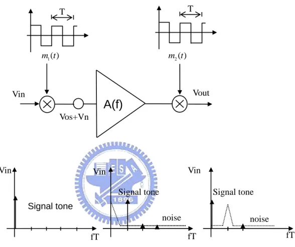
Figure 2.8 The principle of the chopper technique
The input signal is multiplied by the square-wave carrier signalm1(t). After the
modulation, the signal is transposed to the higher frequency. Then the signal in the higher frequency is amplified, at the same time the offset and noise is produced. After amplifying the signal, the signal tone must be modulated to the original spectrum. The noise is modulated to the higher spectrum by m2(t). Therefore, the low frequency
noise can be cancelled since the noise is modulated again.
Vin Vout Vos+Vn
A(f)
) ( 2 t m ) ( 1 t m T T fT fT fT Signal tone Signal tone Signal tone noise noiseFigure 2.9 The principle of chopper in time domain
In the time domain, the input signal is inverted by the first modulation signal as shown in Figure 2.9. After the second modulation clock, the signal is transferred to the original state. In this case, the amplifier gain is infinite, the bandwidth is infinite, and it does not introduce any delay.
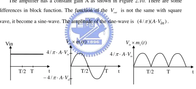
The amplifier has a constant gain A as shown in Figure 2.10. There are some differences in block function. The function of the V is not the same with square out wave, it become a sine-wave. The amplitude of the sine-wave is (4 / )(π A V⋅ in).
Figure 2.10 The principle in the time domain
The modulation technique of CHS is made up of m1(t) . The m1(t) is
modulation signal. The period of the modulation signal is T (1/ fchopper) and its magnitude is 1± as shown in Figure 2.11. The purpose of the modulation signal is to transpose to other bandwidth [30].
Vin Vin×m1(t) Vin×m2(t) T T/2 T/2 T t T/2 T in V A⋅ ⋅ π / 4 in V A⋅ ⋅ −4/π in V A⋅ ⋅ π / 4 t t Vin Vin×m t1( ) 2T T t T 2T T 2T Vin A(Vin) t 1( ) in V ×m t
Figure 2.11 Chopper modulation The Fourier series of the chopper modulation is:
{
}
0 1 2 2 ( ) cos sin n n n n n n f x a a b T T π π =∞ = = + ∑ + (2-4) 1, 0 2 ( ) 1, 2 T x f x T x T ⎧+ < < ⎪⎪ = ⎨ ⎪− < < ⎪⎩ (2-5) The coefficient of a a b : 0, n, n 0 0 1 ( ) 0 T a f x T = ∫ = (2-6) 0 1 2 ( ) cos 0 / 2 T n n a f x xdx T T π = ∫ ⋅ = (2-7) 0 1 2 4 1 ( ) sin / 2 T n n b f x xdx T T n π π = ∫ ⋅ = ⋅ (2-8) Therefore, ( )f x is presented:}
1,3,5,... 4 1 4 1 1( ) sin sin sin 3 sin 5 ..
3 5 n n f x n t t t t n ω ω ω ω π π =∞ = ⎧ = ∑ = ⎨ + + + ⎩ (2-9)
In Equation (2-9), the original signal is modulated to the odd harmonic frequency ( fchopper).The noise is modulated to the odd harmonic frequency, the noise is filter out. The PSD(Power Spectral Density) of the chopped output signal V t is obtained by cs( )
2 2 n 2 1 ( ) ( ) n cs N n odd n S f S f n T π =∞ =−∞ = ⎛ ⎞ = ∑ ⎜ − ⎟ ⎝ ⎠. (2-10)
the low frequency noise and offset voltage are shifted to the odd harmonic.
2.4.2
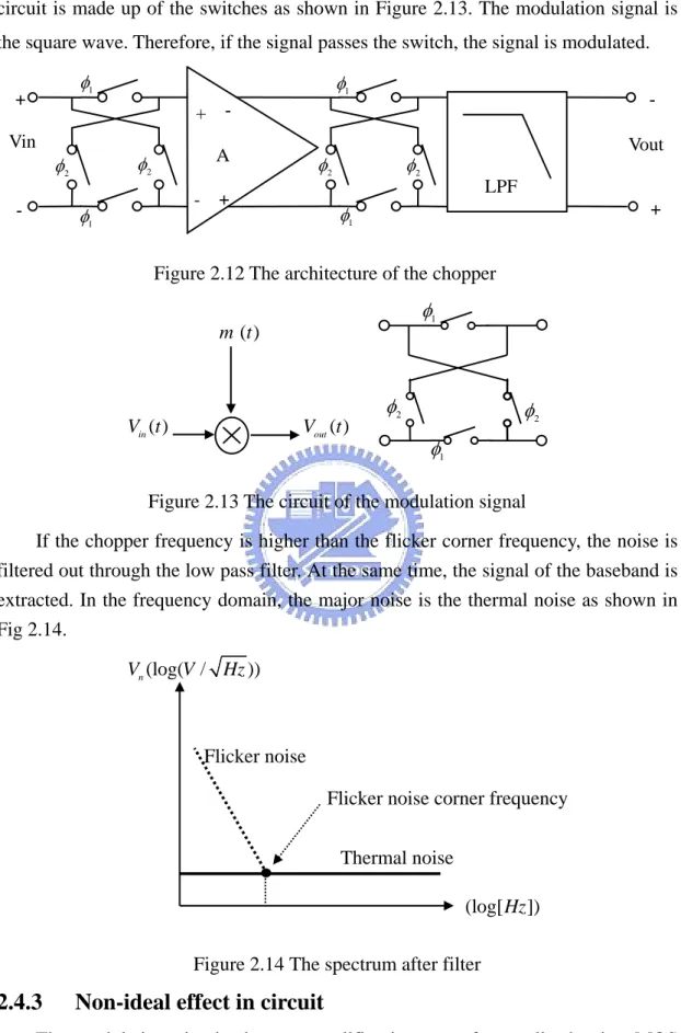
The architecture of the chopper amplifier
In general, there are a gain amplifier, a low pass filter, and a modulation circuit in ) (t m m (t) ( ) N V t VCS( )t -1 +1
the architecture of the chopper amplifier as show in Figure 2.12. The modulation circuit is made up of the switches as shown in Figure 2.13. The modulation signal is the square wave. Therefore, if the signal passes the switch, the signal is modulated.
Figure 2.12 The architecture of the chopper
Figure 2.13 The circuit of the modulation signal
If the chopper frequency is higher than the flicker corner frequency, the noise is filtered out through the low pass filter. At the same time, the signal of the baseband is extracted. In the frequency domain, the major noise is the thermal noise as shown in Fig 2.14.
Figure 2.14 The spectrum after filter
2.4.3 Non-ideal effect in circuit
The modulation circuit chopper amplifier is most often realized using MOS switches. Therefore, no-ideal effect is introduced by the switches. In general, there are
( ) m t ( ) in V t Vout( )t 1 φ 1 φ 2 φ 2 φ 1 φ 1 φ 1 φ 1 φ 2 φ φ2 φ2 φ2 LPF + - Vin Vout A + - -+ - +
Flicker noise corner frequency
(log[Hz]) (log( / )) n V V Hz Flicker noise Thermal noise
two major non-ideal items: clock feedthrough [1], and channel charge injection [1]. When the clock signal is turned off rapidly, the MOS switch couples the noise to the sampling capacitor through its gate-source or gate-drain, as shown in Figure 2.15 [23]. The clock feedthrouth is produced:
Figure 2.15 Clock feedthrough
where C is the sampling capacitor, H V is the clock signal. The errorclk ΔV is : ov ck ov H C W V V C W C Δ = + (2-11) ov
C stands for the overlap capacitance per unit width, V is the magnitude of the ck clock.
Channel charge injection shows in Figure 2.16. When the switch is on, the charge c
Q (2-9) stores in the channel of the switches. When the switch turns off, the charge (Q ) flows to the terminal point (drain or source). If the charge flows to the drain c point with sampling capacitance, the error voltage (ΔV) will appear. In this case, it has an assumption that the quantity of the charge that flow to the drain is only half.
The charge in switch is:
( ) c ox dd in th Q =WlC V −V −V (2-12) H th in dd ox C V V V WlC V 2 ) ( − − = Δ (2-13)
Therefore the error voltage ΔVis the residual voltage. In the chopper amplifier, this phenomenon causes other offset voltage as shown in Figure 2.17.
. Vin Vout Vclk 0 H C
Figure 2.16 Channel charge injection
Figure 2.17 Spike signal of the switch
2.4.4 Practical
Implementation
Issue
In practice, the dummy switch is used to cancel dynamic offset as shown in Figure 2.16. The signal of the switch is accomplished by the clockφ1, and its counter-phase φ . When 1 φ1 of the major switch (S ) is turned off, the channel m charge splits equally to the drain and source terminals. Therefore, the dummy switches with shorted drain and source place in the drain and source. The size of the dummy switch is half of the major switch. The channel charge splits equally to the source and drain.
Figure 2.18 The dummy switch
2 φ 2 φ m S dummy dummy 1 φ spike V + spike V − t T c Q H C Vck Vin Vout
The modulation signal used in differential chopper amplifier is shown in Figure 2.18[3]
Figure 2.19 The NMOS chopper realization
2.5 Summary
In this section, the dynamic offset cancellation is presented. It includes the autozero, correlated double sampling, and chopper stabilization technique. In contrast to the autozero amplifier, the noise of the chopper amplifier is less than the noise of the autozero amplifier. There are other noises which caused by sampling clock in the autozero amplifier. Therefore, the signal in the order of only few μV is suitable for the chopper amplifier to resist the low frequency and offset voltage.
1 φ 2 φ φ2 2 φ 1 φ φ1 2 φ 1 φ φ1 1 φ 2 φ φ2 + -+ Vin Vout
Chapter 3
Design Considerations for
Low-Voltage Low-Power
Chopper Amplifier
3.1 Introduction
Design considerations for low-voltage and low-power chopper amplifier will be discussed in this chapter. First, the MOS transistor working in weak inversion is presented in Section 3.2. The circuits working in weak inversion is designed under the low-power and low-voltage environment. In Section 3.3, the architecture of the filter is introduced. At the end, the clock generator is outlined.
3.2
Weak Inversion in the MOS Transistor
In the region of weak inversion [19] [24], the gate-source voltage is less than the threshold voltage V . Although the gate-source voltage is small, the voltage is still t high enough to create depletion region. In the weak inversion, the channel charge is less than the charge in the depletion region. Therefore, the diffusion current is the
major part of the total current.The drift current is negligible. In contrast to strong inversion, the channel current is the major part of the total current.
Equation (3-1) is the drain current of a MOS in weak inversion [20]:
0 1 exp( ) GS Vt T V nU DS D D T V I I e U − ⎡ ⎤ = ⎢ − − ⎥ ⎣ ⎦ (3-1) Where UT KT q
= is thermal voltage. K is Boltzmann constant
( 23
1.38 10× − J/°K). T is the temperature in degrees Kelvin. q is charge of an electron
( 19
1.6 10× − C). n is the slope factor of the curve. The n is related to the changes in the surface potential Δψs. Δψs is controlled by the oxide capacitance C and the ox depletion-region capacitanceC . Therefore, js
1 s ox GS ox js d C dV C C n ψ = = + . (3-2)
In Equation (3-1), the characteristic current is:
0 ( ) 2 0 2 Vt nUT D T I n U eβ − = (3-3)
Whereβ μ= C W Lox / , μ=electron mobility, and W L are the channel width and channel width.
In Figure 3.1, the weak inversion and strong inversion cure are illustrated. As GS
V below the threshold voltageV , the device is in the weak inversion. In this range, t the curve of the current is exponential (3-1). Above the threshold voltage, the range belongs to the saturation region. In the saturation region, the current is larger than that in the weak inversion. Its current equation is a square function. Therefore, the device in the weak inversion is suitable to low-voltage low-power circuit.
Figure 3.1 MOS weak inversion characteristics
In the weak inversion region, the transconductance can be found by differentiating V [24] [5]. This result is GS
0 1 exp( GS T) 1 exp( DS) D D m D GS T T T T V U V dI W I g I dV L nU nU U nU ⎡ ⎤ − = = ⎢ − − ⎥= ⎣ ⎦ (3-4)
From Equation 3-4, the ratio of the transconductance to the current of an MOS transistor is: 1 m D T g I = nV . (3-5)
In Equation 3-5, the ratio is independent of the overdrive. It is related with the n slop factor (n) and thermal voltage (V ). In contrast to the saturation region, the ratio of the t transconductance to the current is related to the overdrive voltage as show in Equation (3-6) 2 n D 2 2 m D D GS T ov k I g I = I =V − V =V (3-6)
Under the overdrive voltage in strong inversions, gm/I ration is : D 2
ov GS T T
V =V −U = nU (3-7)
The value in Equation (3-7) is about 78 mV when n is 1.5. The ratio of the transconductance to the current versus overdrive voltage is illustrated in Figure 3.2. It is the key point between the strong inversion and the weak inversion.
GS V logID TH V Square Exponential
Figure 3.2 Transconductance to current ratio versus overdrive
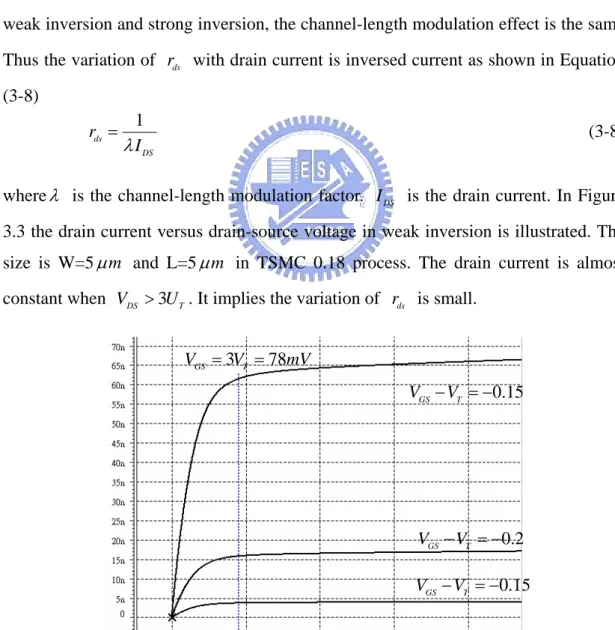
The other parameter of the small signal model is the resistance variation. For weak inversion and strong inversion, the channel-length modulation effect is the same. Thus the variation of r with drain current is inversed current as shown in Equation ds (3-8) 1 ds DS r I λ = (3-8)
whereλ is the channel-length modulation factor. I is the drain current. In Figure DS 3.3 the drain current versus drain-source voltage in weak inversion is illustrated. The size is W=5 mμ and L=5 mμ in TSMC 0.18 process. The drain current is almost constant when VDS >3UT. It implies the variation of r is small. ds
Figure 3.3 Drain current versus drain-source voltage in weak inversion
GS T V −U 2nUT 0 m D g I Weak inversion Strong inversion 0.15 GS T V −V = − 0.2 GS T V −V = − 0.15 GS T V −V = − 3 78 GS T V = V = mV
Next, the mid-band voltage of the common source stage is considered. The mid-band gain is
gain m ds
A = −g r (3-9)
In the strong inversion, the gain varies with I as D
2 D 2 gain D D KI K A I I = = (3-10)
In the weak inversion, the mid-band gain approaches a constant value. It is independent of drain currentI as shown in Equation (3-11). D
1 1 D gain T D T I A nV I nV = = (3-11)
3.3
Filter in Chopper Amplifier
The filter in the chopper amplifier takes an important role. Its purpose is to cancel the noise out of the bandwidth. Therefore, in order to improve the signal to noise ratio, the filter is an important issue. Switched-capacitor filter is introduced latter.
3.3.1
Fundamental of Switched-capacitor circuit
In switched-capacitor circuit is shown in Figure 3.4 [21]. To analyze this circuit,
1
V andV are the DC voltage. When 2 φ1 is on, C is charged to1 V . When 1 φ2 is on,
1
C is charged to V . The 2 φ1 and φ2 are non-overlapping clocks. The charge in capacitor C can be presented with mathematic: 1
(
)
1 1 2
Q C V V
Δ = − (3-12)
The average current I is equal that the charge in the capacitor divides the clock av period. 1( 1 2) av C V V I T − = (3-13)
Figure 3.4 Resistor equivalence of the switched-capacitor
1 φ φ2 1 C 1 V V2 on R 1 V 2 V
At the same time, the equivalent resistor can be shown as: 1 2 av eq V V I R − = (3-14)
Therefore, the equivalent resistor of the switched-capacitor is:
1 1 1 eq s T R C C f = = (3-15)
Switched capacitor integrator is an important role in discrete time integrator [21]. It uses in the switched-capacitor filter or sigma-delta modulator. Usually, parasitic-sensitive integrator and parasitic-insensitive integrator are introduced.
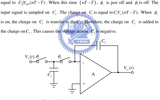
The parasitic-sensitive integrator is shown in Figure 3.5. At the time
(
nT−T)
, the voltage across the capacitor C is 2 Vco(nT−T). Therefore, the charge on C is 2 equal to C V2 co(nT−T). When this time(
nT−T)
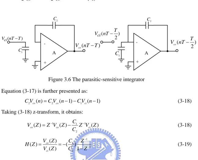
, φ1 is just off and φ2is off. The input signal is sampled on C . The charge on 1 C is equal to1 C V nT1 ci( −T). When φ2 is on, the charge on C is transfer to the1 C . Therefore, the charge on 2 C is added to 1 the charge onC . This causes the voltage across 2 C is negative. 2Figure 3.5 Parasitic-insensitive integrator In Figure 3.6 the behavior during φ1 and φ2 is illustrated. This phenomenon is presented by mathematical equation:
2 ( ) 2 ( ) 1 ( )
2
co co ci
T
C V nT− =C V nT−T −C V nT−T (3-16)
At the end of the next φ1, the charge on C at time 2
( )
nT is equal to the charge at time 2 T nT ⎛ − ⎞ ⎜ ⎟⎝ ⎠. It can be shown as:
1 φ φ2 1 C 2 C ( ) ci V t ( ) co V t A -+
2 co( ) 2 co( ) 1 ci( )
C V nT =C V nT−T −C V nT−T (3-17)
Figure 3.6 The parasitic-sensitive integrator Equation (3-17) is further presented as:
2 co( ) 2 co( 1) 1 ci( 1)
C V n =C V n− −C V n− (3-18) Taking (3-18) z-transform, it obtains:
1 1 1 2 ( ) ( ) ( ) co co ci C V Z Z V Z Z V Z C − − = − (3-18) 1 1 1 2 ( ) ( ) ( ) ( ) 1 co ci V Z C Z H Z V Z C Z − − = = − − (3-19)
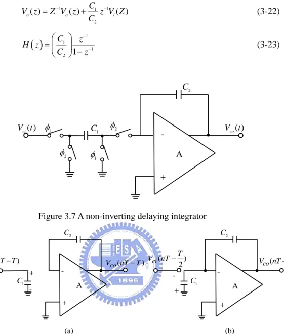
The parasitic-insensitive integrator is a critical circuit to develop high-accuracy circuit. As its name, it is insensitive to parasitic capacitor [21]. Therefore, the parasitic-insensitive integrator is usually used for high-order high-resolution circuits,.
The parasitic-insensitive integrator is made up of four switches as shown in Figure 3.7. When φ1 is on, C is charged to 1 C V nT1 ci( −T). Then C turns on, the 2 charge on C discharge to the 1 C . At this moment, the output voltage is positive. 2
In Figure 3.8 it can be presented in mathematical:
2 ( ) 2 ( ) 1 ( )
2
co co ci
T
C V nT− =C V nT−T +C V nT−T (3-20) At the end of next time (nT), the charge on C is the same at the time 2 (
2 T
nT− ). Therefore, the Equation (3-20) is:
C V2 co(nT)=C V2 co(nT−T)+C V nT1 ci( −T) (3-21) Its z-transform is presented:
( ) ci V nT T− ( ) 2 ci T V nT− 1 C 2 C 2 C A - + -+ A 1 C ( ) 2 co T V nT− ( ) co V nT−T
1 1 1 2 ( ) ( ) ( ) o o i C V z Z V z z V Z C − − = + (3-22)
( )
1 1 1 2 1 C z H z C z − − ⎛ ⎞ = ⎜ ⎟ − ⎝ ⎠ (3-23)Figure 3.7 A non-inverting delaying integrator
Figure 3.8 Behavior in each clock (a)φ1 ,(b)φ2
There is another parasitic-insensitive integrator as shown in Figure 3.9. It is different from the non-inverting integrator. When clock φ1 is on, the capacitor is charged to Vci( )t . Then the charge passes through C to change the amount of the 2 output voltage. In other words, when φ2 turns on, the charge across C is the same 2
as the old charge. It stands for 2 ( ) 2 ( ) 2
co co
T
C V nT− =C V nT−T , so its behavior and the z-transform are introduced.
2 ( ) 2 ( ) 1 ( ) 2 co co ci T C V nT =C V nT− −C V nT (3-24) 2 co( ) 2 co( ) 1 ci( ) C V nT =C V nT−T −C V nT (3-25) ( ) ci V nT T− 1 C -+ 2 C ( ) co V nT−T ci( 2) T V nT− 1 C + -2 C ( ) 2 co T V nT− A - + A - (a) (b) + 2 φ 2 φ 2 C 1 C ( ) ci V t V tco( ) A -+ 1 φ 1 φ
1 1 2 1 ( ) 1 C H z C z− ⎛ ⎞ = −⎜ ⎟ − ⎝ ⎠ (3-26)
Figure 3.9 Delay-free integrator
3.3.2 The Architecture of Filter
Next, the architectures of the filter are introduced. It includes the first-order and second-order filter .
A first-order active-RC filter is shown in Figure 3.10. The resistors are replaced with delay-free switched capacitors. Therefore, the discrete-time first-order filter is illustrated as shown in Figure 3.11.
Figure 3.10 A first-order active-RC filter According to the Figure 3.11 the transfer function is:
1 1 3 2 1 (1 ) ( ) ( ) (1 ) ( ) A o o i i C −z− V = −C V z −C V z −C −z− V z (3-27) 2 C 1 φ 1 φ 2 φ φ2 1 C ( ) ci V t V tco( ) A -+ A -+ ( ) in V s ( ) in V s
1 2 1 3 ( ) ( ) ( ) (1 ) 1 A A o i A C C C z C C V z H z C V z z C ⎛ + ⎞ − ⎜ ⎟ ⎝ ⎠ = = − + − (3-28)
Figure 3.11 Discrete-time form
Next section, the architecture of the second-order filter is introduced. The one is the low-Q biquad filter, the other is high-Q biquad filter. These filters are made up of inverting integrator and non-inverting.
First, the architecture of the low-Q biquad filter is illustrated in Figure 3.12. According to the block diagram, the transform function of the architecture is illustrated. It design the coefficient according to the specification. The discrete-time architecture is illustrated in Figure 3.13. In Figure 3.12 the transfer function is
2 2 1 0 2 0 2 0 ( ) ( ) ( ) ( ) out in V s k s k s k H s V s s Q ω+ +ω = = + + (3-29)
The z-transfer function is shown as Figure 3.13:
2 2 3 1 5 2 3 3 6 4 5 6 ( ) ( 2 ) ( ) (1 ) ( 2) 1 k k z k k k k k H z k k k k + + − − + = − + + − − + (3-30)
According to the equations, designing filter is done.
1 φ φ1 2 φ 2 C C3 1 C A C ( ) i V z V zo( ) A -2 φ 1 φ φ1 2 φ φ2 +
Figure 3.12 The block diagram of the biquad filter
Figure 3.13 A low-Q switched capacitor biquad filter
The other architecture of the filter is high-Q biquad filter as shown in Figure 3.14 This value of Q in this architecture is limited to 5 or less. The elements in high-Q biquad filter is not too large. If the element is too large, it may be not realized. The transfer function of the high-Q biquad filter is shown as Equation (3-29). To replace resistor with switched-capacitor integrator, the architecture of the discrete-time form
1 φ 1 φ 2 φ φ2 1 φ φ1 2 φ φ2 1 φ 1 φ 2 φ 2 φ 1 1 k C 1 C 2 2 k C 3 2 k C 2 C 5 2 k C 4 1 k C 6 2 k C ( ) i V z ( ) i V z - + -+ A 1 φ φ1 2 φ φ2 1 φ φ1 2 φ φ2 A 1 s − 1 s − o ω o ω − / o o k ω ( ) in V s Vout( )s 1 2 k +k s
is described as shown in Figure 3.15
Figure 3.14 The high-Q biauad filter
Figure 3.15 High-Q switched-capacitor biquad filter
Taking the z-transform in Figure 3.15, the transform function of the high-Q filter is
(
) (
)
(
) (
)
2 3 1 5 2 5 3 3 2 5 2 4 5 5 6 5 6 2 ( ) ( ) ( ) 2 1 o i k z k k k k k z k k k V z H z V z z k k k k k k + + − + − = = − + + − + − (3-31)According to Equation (3-29) (3-31), the switched-capacitor filter is designed for the specification. ( ) o V z ( ) i V z 1 1 k C 2 2 k C 3 2 k C 5 2 k C 6 2 k C 2 C 1 C -A + - A + 1 φ φ1 2 φ φ2 1 φ 1 φ 2 φ 2 φ 1 φ φ1 2 φ φ2 4 2 k C 2 k s 1 / 0 k s ω 1 s − 1 s − / o o k ω o ω / S Q ( ) out V s ( ) in V s
3.4 Low-Voltage Switch
At low supply voltage, it is difficult to drive the switch. Under this condition, the overdrive voltage is lower than threshold voltage. The switch is not open entirely. The signal must have some loss, it is a serious problem in sampling circuit. How to drive the switch at low supply voltage must be solved. The switch conductance for different input depending on supply voltage is illustrated in Figure 3.16. In Figure 3.16 (a) it is at standard voltage, Figure 3.16 (b) at low supply voltage.
Figure 3.16 Transmission gate conductance at (a) standard, (b)low supply voltage Low threshold voltage is one of the solution to be solved the switch at low
supply voltage. The threshold voltage is given by
2 2 ox th GB F F BS ox Q V V C φ φ γ φ = − + + − (3-32)
The above equations show that theV depends onth V . The bulk to source BS junction causes the threshold voltage increase due to the body effect. So in order to drive switches at low supply voltage, the threshold voltage needs to be decreased. Therefore, the body effect reversed, the threshold voltage can be decreased.
However, decreasing the threshold voltage causes another problem. When switch is off, there is leakage current between bulk and source. If this condition happens, the resolution of this circuit must lower. Non-ideal items is hard to be expected.
The voltage multiplier is another technique. It converts the lower voltage to higher voltage. In higher supply voltage, the overdrive voltage is higher enough to
NMOS NMOS PMOS PMOS ds g min ds g thp V Vdd −VthnVdd swing ov V Vov min ds g in V ds g dd thn V −V Vthp swing swing ov V Vov
drive the switch. The aliasing phenomenon can be decreased. Figure 3.17 shows a voltage boosted clock driver. Fist, C and 1 C are charged to 2 V which passes dd through cross-coupled NMOS M1 and M2. When clock input signal, goes high, the output voltage must be pushed to 2V . However, the output voltage can not dd achieve 2V , in transition time charge sharing happens. So the capacitor dd C must be 2 large enough, charge sharing effect will be decreased little. On the side, latch-up can be avoided; the voltage doubler is used as shown in Figure 3.18. The bulk of the PMOS M3 is tied to a voltage doubler.
Figure 3.17 Voltage boosted clock driver
CK dd V sw CK bulk V 1 C C2 2 M 1 M 3 M
Figure 3.18 Voltage doubler
3.5 Summary
In this chapter, the MOS transistor working in weak inversion, switched- capacitor circuits, and low-voltage switch techniques are introduced. There are the elements in the chopper amplifier. In order to work at low supply voltage, the MOS working in weak inversion is needed. The switch working at low supply voltage is another important issue. Summing up this issue, how to design a low-voltage low-power circuit is a critical thing.
dd V bulk V CK 1 C 2 C 2 M 1 M
Chapter 4
The Front-end Circuit
of the Thermopile
4.1 Introduction
The MOS transistor working in weak inversion, switched-capacitor filter, and switches at low supply voltage are introduced in the previous chapter. Some of them are used in this thesis. The amplifier working in weak inversion is necessary for low supply voltage. The MOS working in strong inversion is not realized under low supply voltage. In contrast to strong inversion, weak inversion is suitable for low supply voltage. The amplifier working in weak inversion is used in switched-capacitor filter, preamplifier, and post-amplifier. On the side, the total architecture is illustrated. The preamplifier, switched-capacitor filter, and post-amplifier are introduced detail. The noise of the preamplifier is also carefully calculated in this chapter. Finally, the front-end circuit of the thermopile sensor (preamplifier, filter, and post-amplifier) is realized in this thesis.
4.2 System
Architecture
preamplifier, filter, and post-amplifier are the parts of architecture. The front of the chopper amplifier is a thermopile sensor. The thermopile sensor detects the temperature to transfer to the voltage. Then the voltage passes through chopper amplifier, filter, and ADC. Finally, the signal is transferred to digital form [3] [14].
The block diagram is shown in Figure 4.1
Figure 4.1 Block diagram of the temperature sensor
Sensor Signal In this thermopile sensor, the signal specification is: Type: voltage
Temperature range: 32 ~ 44° ° Signal magnitude: 10μV / 0.2° C Signal bandwidth: 50Hz
The output voltage rang of the thermopile sensor is from 10 Vμ to 600 Vμ . This signal magnitude is only a few micro volts. The noise power must not be too large under this condition. In this thesis, the system resolution is 8-bit. When the resolution is 8-bit, the signal to noise ratio is worked out. Its value is approximately 50db. According to signal to noise ratio (SNR) the noise power is calculated as [6]
600 20 log 50 2 rms V SNR db N μ = × = ⋅ . (4-1)
The noise root mean square is approximately 1.38 Vμ . Therefore, the noise root mean square can not be over 1.38 Vμ in the output of the sensor.
Chopper Amplifier Due to the magnitude of the sensor signal is too small, and the bandwidth is DC value, the signal to noise ratio does not achieve the specification [5]. The chopper amplifier is used to cancel the low frequency noise to increase the signal to noise ratio. Therefore the gain of the system must be another issue. Thinking about
Chopper Amplifier ( ) m t m t( ) LPF Vout sensor
signal to noise ratio, the gain of the system must achieve to 60db. The open loop amplifier is used in this block
Low Pass Filter In this architecture, the purpose of the low pass filter is used to cancel the noise [7] [4]. According to the noise root mean square value, the second-order switched capacitor filter is implemented. In this low pass filter, its pass band frequency is 50hz, and its stop-band frequency is 500hz. Due to this specification, the total noise power is integrated in this spectrum range. The value is the total noise power.
4.3
Implementation of Chopper Amplifier
The chopper amplifier is the first stage. The first stage is an important element in all system. The noise power behind the chopper amplifier can be negligible. Because the gain of the chopper amplifier is large, the input referred noise changes small. So the major noise is produced in the first stage. Therefore the flicker noise and thermal noise comes from the first stage are considered. The chopper amplifier can cancel low frequency noise (flicker noise). Therefore the thermal noise dominants noise power. How to decrease the noise power is important.
4.3.1 Noise
Consideration
In order to consider the thermal noise of the amplifier, the noise model must be considered. In Chapter 2, the noise of the MOS transistor is brought out. It includes the thermal noise and flicker noise. The noise model can be shown in Figure 4.2
Figure 4.2 Noise model
The equivalent model includes flicker and thermal noise. The noise divides by 2
m g to the input. Hence, the PSD of an equivalent input noise is calculated as
2 ( ) g V f 2 ( ) d I f 2 ( ) i V f
8 1 ( ) 3 f eq ox k S f kT gm WLC f = + . (4-2)
According to the equivalent input noise, the input referred noise in amplifier is illustrated. Each noise of the MOS transistor is independent each other. Therefore, they are uncorrelated. Next, current mirror and telescopic circuit working in weak inversion are discussed. Figure 4.3 shows the total noise source in current mirror amplifier [7].
Figure 4.3 Noise analysis The 2
n
V includes the flicker noise and thermal noise. First, the thermal noise is only calculated. The V is shown as n2 8
3 m KT
g . The total thermal noise power is presented
2 2 2 2 2 2 2 2 2 , 1 ( 1 ) 3 ( 3 ) 5 ( 5 ) 7 ( 7 )
o total n m out n m out n m out n m out
V =V g r +V g r +V g r +V g r
2 2 2 2 2 2 2 2 2 ( 2 ) 4 ( 4 ) 6 ( 6 ) 8 ( 8 )
n m out n m out n m out n m out
V g r V g r V g r V g r
+ + + + (4-2)
Because the circuit is symmetry, the total noise power can be presented as
2 2 2 2 2 2 2 2 2 , 2( 1 ( 1 ) 3 ( 3 ) 5 ( 5 ) 7 ( 7 ) )
o total n m out n m out n m out n m out
V = V g r +V g r +V g r +V g r (4-3)
The V is replaced byn2 8 3 m
KT
g , the Equation (4-3) is shown as:
2 2 2 , 1 3 1 3 8 8 2( ( ) ( ) 3 3
o thermal m out m out
m m kT kT V g r g r g g = + 2 6 n V 2 4 n V 1 M M2 3 M M4 5 M M6 7 M M8 2 1 n V Vn22 2 3 n V 2 5 n V 2 7 n V 2 8 n V on V Vop ip V in V
2 2 5 7 5 7 8 8 ( ) ( ) ) 3 m m out 3 m m out kT kT g r g r g g + + (4-4)
The Equation (4-4) is divided by
(
g Rm1 out)
2, therefore the total input referred thermal noise spectral density is:2 , 3 5 7 1 1 1 1 16 ( ) 1 3 m m m i total m m m m g g g kT V f g g g g ⎛ ⎞ = ⎜ + + + ⎟ ⎝ ⎠. (4-5)
Second, the flicker noise is considered. The output noise spectral density is
(
)
2 2 2 , ker 1 3 1 1 3 3 ( ) f fo flic m out m out
ox ox k k V g r g r f C W L f C W L = + ⋅ ⋅
(
5)
2(
7)
2 5 5 7 7 f f m out m out ox ox k k g r g r f C W L f C W L + + ⋅ ⋅ (4-6)The input referred noise can be shown as:
2 2 3 , ker 1 1 2 2 1 1 f f m i flic ox ox m k k g V f C W L f C W L g ⎛ ⎞ = ⋅ + ⎜ ⎟ ⋅ ⋅ ⎝ ⎠ 2 2 5 7 5 5 1 7 7 1 f m f m ox m ox m k g k g f C W L g f C W L g ⎛ ⎞ ⎛ ⎞ + ⎜ ⎟ + ⎜ ⎟ ⋅ ⎝ ⎠ ⋅ ⎝ ⎠ (4-7)
The flicker corner noise frequency is presented, when the flicker noise is equal to the thermal noise as V2i theraml, =V2i flic, ker. According to the Equation (4-5) and (4-7), the flicker noise corner frequency is obtained.
In the telescopic amplifier, the noise is analyzed. The manner is the same with current mirror amplifier. In Figure 4.4, the noise in the telescopic amplifier is shown as
Figure4. 4 Noise analysis in telescopic current The input referred flicker and thermal noise are shown as
2 3 , 1 1 16 ( ) 1 3 m i thermal m m g kT V f g g ⎛ ⎞ = ⎜ + ⎟ ⎝ ⎠ (4-8) 2 2 3 , ker 1 1 2 2 1 1 f f m i flic ox ox m k k g V f C W L f C W L g ⎛ ⎞ = ⋅ + ⎜ ⎟ ⋅ ⋅ ⎝ ⎠ (4-9)
In a word, the thermal and flicker noise are shown in MOS circuit.
In Section 4.2, the noise power is calculated. The filter bandwidth is set. Because the chopper amplifier cancel the flicker noise, the thermal noise dominants the total noise power. The noise bandwidth is known form the filter bandwidth, the thermal noise power is obtained. The current mirror amplifier is taken as example. The gm1 is calculated. First, the gm is equal each other. Second, the thermal noise power spectral density is calculated 80nV/ Hz in due to filter bandwidth. Therefore the transconductance gm can be presented as:
2 3 5 7 2 , 1 1 1 1 16 ( ) 1 (80 ) 3 m m m i theraml m m m m g g g kT V f nV g g g g ⎛ ⎞ = ⎜ + + + ⎟= ⎝ ⎠ (4-10)
According to Equation (4-10), gm is 13.8μA V/ . Therefore the gm must be less than 13.8μA V/ .
4.3.2
Noise Efficient Factor
2 4 n V 1 M M2 3 M M4 2 1 n V Vn22 2 3 n V on V op V ip V in V dd V
We are interested in minimizing noise in strict power. They are tradeoff between noise and power. Noise efficient factor is considered. Noise efficient factor is related with noise and power. According to noise efficient factor, we distinguish between differential architectures. The noise efficient factor is introduced in Equation (4-11).
, 2 4 total ni rms T I NEF V V kT BW π = ⋅ ⋅ ⋅ . (4-11)
Where Vni rms, is the input-referred rms noise voltage. Itotalis the total current. BW is the amplifier bandwidth. VTis the thermal voltage.
The noise efficient factor is an important factor. It is used to designing the chopper amplifier. The value of the NEF is smaller, the chopper amplifier is better.
4.3.3 Figure of Merit
There is another index to design chopper amplifier. The amplifier focused on noise and low supply voltage. Therefore, the figure of merit focused on noise, power and area, the equation is
1 FOM
N S P =
× × . (4-12)
Where N is the noise density. P is the power dissipation. S is the chip area. According to the FOM[8], the tradeoff between cost and power dissipation is distinguish. In contrast to the NEF (noise efficient factor), the FOM (figure of merit) focus on area. Therefore the cost is considered.
4.3.4 Summary
In order to design the chopper amplifier efficiently, the factors as NEF, FOM are considered. On the side, the SNR is another issue. Therefore, the signal before ADC must be large to suit to the specification. The signal must be large than 0.5v to achieve SNR. The gain of the system must be large 60db. The gain can be divided as Table 1
Pre-amplifier
Post-amplifier
Type 1
60db
0db
Type 2
50db
10db
Type 3
40db
20db
Type 4
30db
30db
The best type is chosen. Because the chopper amplifier is modulation signal, the chopper amplifier must be faster than the modulation signal. First, we assume that the modulation signal clock is 10k hz, the chopper amplifier must be faster than the 10k hz.
This key point lists following to design the chopper amplifier (1) The unity gain frequency,
(2) Thermal noise value, (3) Flicker noise,
(4) Flicker noise corner frequency, (5) Slew rate,
(6) Noise efficient factor, (7) Figure of merit.
Integrating with these rules, the chopper amplifier is designed. The design flow is illustrated as shown in Figure 4.5. First, the unity gain frequency is decided, then the transconductance and current is found. Next, the slew rate of amplifier is checked. If the slew rate is suitable for the specification, the flow can continuous. However the slew rate may be not suitable for the specification. In this condition, the flow must be return to start. When the slew rate is completed, next step decide the MOS transistor size. Finally, the noise efficient factor and figure of merit are calculated. In this flow, the size of the differential pair is considered in the FOM.
The noise efficient factor and figure of merit are the bases of the amplifier comparison. According to the parameter, the gain of the first stage can be distinguished. The parameter of the current mirror and telescopic amplifier are listed in Table 2. In Table 2, the gain of each block is decided and the telescopic amplifier is design in the first stage .
Figure 4.5 The design flow
First Stage
gm(
μV A/)
Id( )
nANoise
(
nV/ Hz)
NEF FOM
60db 125 4.875
26
4.3 4.598
50db 39 1.521
50
4.6 23
40db 12 0.486
85
4.5 73
35db 89 0.347
99
4.5 232
Table 2 Current mirror type T f gm d I Noise corner W,L SR NEF FOM Start NO YES
Table 3 The telescopic amplifier type
Table 2 and Table 3 are suitable for the slew rate. Therefore, the solution is suitable for the specification. Last, we choose that the gain is 40db in first stage.
4.4 Filter Design
4.4.1 System Architecture
According to the signal bandwidth, the pass-band frequency is 50 hz. In this thesis the filter type is butterworth. Its characteristic of the butterworth is flat in pass bandwidth and stop bandwidth. The transfer function of the second-order low pass filter is shown as 2 ( ) 98596 ( ) ( ) 444 98596 o i V s H s V s s s = = + + . (4-13)
The Bode Diagram of the transfer function is shown as Figure 4.6
Figure 4.6 The Bode Diagram