Design of an UWB CMOS LNA for 3.1 to
10.6 GHz with RL-feedback
:
:
Design of an UWB CMOS LNA for 3.1 to 10.6 GHz
with RL-feedback
Design of an UWB CMOS LNA for 3.1 to
10.6 GHz with RL-feedback
Student: Hung-Wei Wang
Advisor: Dr. Albert Chin
Department of Electronics Engineering & Institute of Electronics
Nation Chiao Tung University
Abstract
A 3.1-10.6 GHZ low noise amplifier is applied for ultra-wideband, it introduces
RL feedback for input matching. And current buffer is used for output matching. This
research is fabricated in 0.18- m CMOS process. Three amplified stages are formed
for main topology in low noise amplifier. The first stage introduces RL-feedback
configuration, it can improve the bandwidth. The second stage introduces traditional
CS configuration, it can improve the average forward S21. The third stage introduces
current buffer configuration, it is used for output matching. Relatively flat gain is
essential over the entire desired band. The low noise amplifier introduces the shunt
peaking to achieve the above purpose. The total power dissipation of the chip is about
29 mW at power supply 1.8 volt. The chip size included pad is 0.776 mm2. The
measurement result of this study expect that the average forward S21 is 6.9dB at
3.1-10.6GHz, the reverse isolation S12 is under -33dB, the magnitude of S11 is under
Contents
Abstract (in Chinese)
………IAbstract (in English)
………...II…………...………III
Contents
……….IVFigure Captions
……….VIChapter 1 Introduction
1.1 UWB CMOS Receivers
………..………….….11.2 Motivation
………2Chapter 2 Issues in RFIC Design
2.1 Noise Analysis
2.1.1 The Concept of Noise Figure………4 2.1.2The Noise Figure of an Amplifier Circuit……….6
2.2 Linearity in RF Circuit
………..9 2.2.1 Third-Order Intercept point and The 1-dB Compression Point…………...11 2.2.2 Cascaded Nonlinear Stages……….14Chapter 3 Basic LNA Design
3.1 Consideration in Low-Noise Amplifiers
3.1.2 Stability………25
3.2 Wide-band LNA design
………...27Chapter 4 UWB CMOS LNA Design
4.1
Design Procedures
………...324.1.1 Inductor-Resistance Feedback……….35
4.1.2 Shunt Peaking………..39
4.2 Simulation Results
………414.3 Measurements and Conclusions
………45Chapter 5 Summary
………...50References
……….51Figure Captions
Chapter 1 Introduction
Chapter 2 Issues in RFIC Design
Figure 2-1 Input-referred noise model for device.
Figure 2-2 Plot of input output power of fundamental and IM3 versus input power.
Figure 2-3 Cascaded nonlinear stages.
Chapter 3 Basic LNA Design
Figure 3-1 Circuit embedded in a 50 .
Figure 3-2 Circuit embedded in a 50 .
Figure 3-3 Example of a very sample matching network.
Figure 3-4 A possible impedance-matching network.
Figure 3-5 The eight possible impedance-matching networks with two reactive
components.
Figure 3-6 Which ell matching networks will work in which regions.
Figure 3-7 Stability of two-port networks.
Figure 3-8 Wide-band LNA circuit schematic.
Figure 3-10 Small-signal equivalent circuit at the input.
Chapter 4 UWB CMOS LNA Design
Figure 4-1 Circuits diagram.
Figure 4-2 Chip layout.
Figure 4-3 Parallel resonance circuits.
Figure 4-4 C-S amplifier with source degeneration.
Figure 4-5 A source degeneration amplifier with inductor-resistor feedback.
Figure 4-6 The equivalent circuit of source degeneration amplifier with
inductor-resistor feedback.
Figure 4-7 The model of shunt peaking amplifier.
Figure 4-8 Simulated S11&S22.
Figure 4-9 Simulated S21.
Figure 4-10 Simulated NF.
Figure 4-11 Simulated S12.
Figure 4-12 Simulated stability.
Figure 4-13 Two tones test.
Figure 4-14 Measured S21.
Figure 4-16 Measured S11.
Figure 4-17 Measured S22.
Figure 4-18 Measured noise figure.
Figure 4-19 Measured linearity.
Chapter 1
Introduction
1.1 UWB CMOS Receivers
UWB (Ultra Wideband) is a ring in the wireless communication field. Main
application 10 about short distance high-speed communication, and more than 100
metres, even 1 kilometer one communicate at a low speed remotely. If compare UWB
and 802.11a, pure according to view on technology, the high transfer rate of UWB
and power of low consumption are superior to 802.11a . UWB can allow to convey
the materials of 500 Mega Bits per second in (about five metres ) range of 15 feet , in
other words, UWB is the specification of conveying a large number of materials in the
short distance, another advantage of UWB is that the power consumption is very low.
The FCC has allocated 7.5 GHZ of spectrum for unlicensed use of UWB devices in
the 3.1 to 10.6 GHZ frequency band. The low noise amplifier needs to amplify the
received UWB signal with sufficient gain and as little as possible.
The majority implementation of the RF integrated circuit used for wireless
devices are encounter with various possibilities: CMOS, Bi CMOS, and GaAs
MESFET, bipolar (BJT), hetero-junction bipolar transistor (HBT), and PHEMT, etc,.
We just focus on the CMOS technology, CMOS process reduce the minimum channel
For example, a deep sub-micron prototype CMOS technology has realized devices
with ft exceeding 100 GHz [1] and minimum noise figures less than 0.5-dB at 2 GHz.
The more commercially available sub-micron CMOS technologies have display ft’sof
20GHz and minimum noise figures of 1.6-dB at 2Ghz [2]. The VLSI capabilities of
CMOS make it proper to very high levels of mixed signal radio integration while
increasing the functionality of a single chip radio to cover multiple RF standards [3].
Due to the advancement of circuit design technology, circuit size is small and cost
down consideration. With the work at [4] [5] [6], low cost and low power devices of
RF front-end system implemented by CMOS technology, the prospect of a single chip
CMOS system has received considerable interest. Even the SOC is difficult and hard
to implement at this time, but a set of separate chips in the same CMOS technology
may bring significant economic benefits [7].
1.2 motivation
For portable wireless communication devices has given great push to the
development of a next generation of low power radio frequency integrated circuits
(RFIC) product. Such as wireless phones, cordless and cellular, global positioning
satellite (GPS), pagers, wireless modems, wireless local area network (LAN), and RF
ID tags, etc., require more low cos and high power efficiency solutions to
Chapter 2 discusses the basic concepts in RF design. Chapter 3 presents the
basic low-noise amplifiers design for UWB. Chapter 4 deals with wideband matching
network by using inductor-resistor feedback, presents the UWB proposals, design,
implementation of a low-noise amplifier. Chapter 5 concludes this research effort with
Chapter 2
Issues in RFIC Design
2.1 Noise Analysis
2.1.1 The Concept of Noise Figure
Noise is usually generated by the random motions of charges or charge carriers
in devices and materials. Because the noise process is random, one cannot identify a
specific value of voltage at a particular time, and the only recourse is to characterize
the noise with statistical measures, such as the mean-square or root-mean-square
values. Because of having various noise sources in the circuit, we need to simplify
calculation of the total noise at the output [9]. Obviously, the output-referred noise
does not allow a fair comparison of the performance of different circuits because it
depends on the gain. According the circuit theory, we can use the input-referred noise
of circuits to represent the noise of behavior in the circuits.
The signal-to-noise ratio (SNR), defined as the ratio of the signal power to the
total noise power, is an important parameter. In RF circuit, most of the front-end
receiver blocks are characterized in terms of their “noise figure” rather than the
input-referred noise. Noise figure has many different definitions. The most commonly
accepted definition is
Noise figure is a measure of how much the SNR degrades as the signal passes through
a circuit. If a circuit has no noise source, the SNRout=SNRin, regardless of the gain.
Noise added by electronics will be directly added to the noise from the input.
Thus, for reliable detection, the previously calculated minimum detectable signal level
must be modified to include the noise from the active circuitry. Noise from the
electronics is described by noise factor F, which is a measure of how much the
signal-to-noise ratio is degraded through the system. We note that
S
G
S
o = ⋅ i (2.2) where S is the input signal power, i S is the output signal power, and G is the o power gain So Si. We derive the following equation for the noise factor:) ( ) ( 0 ) ( ) ( ) ( ) (
)
(
i source total total o i source i i total o o source i i o iN
G
N
N
G
S
N
S
N
S
N
S
SNR
SNR
F
⋅
=
⋅
=
=
=
(2.3)where No(total) is the total noise at the output. If No(source) is the noise at the output
originating at the source, and No(added) is the noise at the output added by electronic circuitry, then we can write:
) ( )
( )
(total o source o added
o
N
N
N
=
+
(2.4) Noise factor can be written in several useful alternative forms:) ( ) ( ) ( ) ( ) ( ) ( ) ( ) ( ) (
1
source o added o source o added o source o source o total o source i total oN
N
N
N
N
N
N
N
G
N
F
=
=
+
=
+
⋅
=
(2.5)This shows that the minimum possible noise factor, which occurs if the
electronics add no noise, is equal to 1. Noise figure NF is related to noise factor F by
F
NF
=
10
log
10 (2.6) Thus, while noise factor is at least 1, noise figure is at least 0 dB. In other words, an electronic system that adds no noise has a noise figure of 0 dB.In the receiver chain, for components with loss (such as switches and filters), the noise figure is equal to attenuation of the signal. For example, a filter with 3 dB of loss has a noise figure of 3 dB. This is explained by noting that output noise is approximately equal to input noise, but signal is attenuated by 3 dB. Thus, there has degradation of SNR by 3 dB. [10]
2.1.2 The Noise Figure of an Amplifier Circuit
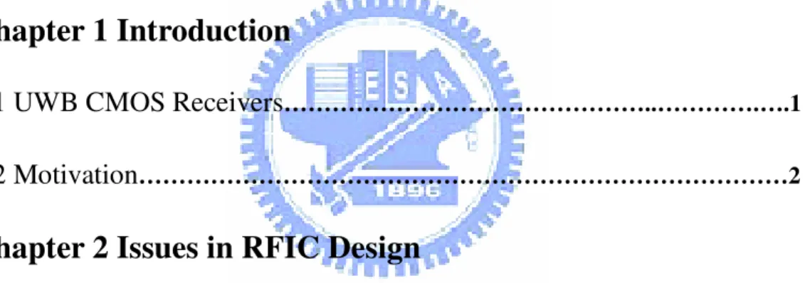
Now, we can make use of the definition of noise figure just developed and apply it to an amplifier circuit. For the purposes of developing (2.5) into a more useful form, it is assumed that all practical amplifiers can be characterized by an input-referred noise model, such as shown in Figure 2-1, where the amplifier is characterized with current gain Ai. In this model, all noise sources in the circuit are lumped into series noise voltage source νn in
s Y 2 2 2 2 ns in in
i
i
SNR
α
α
=
(2.7)Assuming that the input-referred noise sources are correlated, the output signal-to-ratio is
)
(
2 2 2 2 2 2 2 s n n ns i in i outY
i
i
A
i
A
SNR
ν
α
α
+
+
=
(2.8)Thus, the noise factor can now be written in terms of the preceding two equations:
(
)
(
source)
o total o ns s n n nsN
N
i
Y
v
i
i
F
=
+
2+
=
2 2 (2.9) This can also be interpreted as the ratio of the total output noise to the total output noise due to the source admittance.In (2.8), it was assumed that the two input noise source were correlated with each other. In general, they will not be correlated with each other, but rather the current in will be partially correlated with vn and partially uncorrelated. We can expand both current and voltage into these two explicit parts:
u
c
n
i
i
i
=
+
(2.10)u
c
n
v
v
v
=
+
(2.11)In addition, the correlated components will be related by the ratio
c
c
c
Y
v
i
=
(2.12)where Yc is the correlation admittance. The noise figure can now be written as
2 2 2 2 2 2
1
ns s u c s c ui
Y
v
v
Y
Y
i
NF
=
+
+
+
+
(2.13)The noise current and voltages can also be written in terms of equivalent resistance and admittance:
f
kT
v
R
c c∆
=
4
2 (2.14)f
kT
v
R
u u=
∆
4
2 (2.15)f
kT
i
G
u u∆
=
4
2 (2.16)f
kT
i
G
ns s∆
=
4
2 (2.17)s u s c s c u
G
R
Y
R
Y
Y
G
NF
2 21
+
+
+
+
=
(2.18)(
) (
)
[
]
(
)
s u s s c s c s c uG
R
B
G
R
B
B
G
G
G
NF
2 2 2 21
+
+
+
+
+
+
+
=
(2.19) It can be seen from this equation that NF is dependent on the equivalent source impedance. [10]For a cascade of stages, the overall noise figure can be obtained in terms of the NF and gain of each stage. For m-stages, the NFtot is equal to
) 1 ( 1 1 2 1
1
1
)
1
(
1
−−
+
+
−
+
−
+
=
m p p m p totA
A
NF
A
NF
NF
NF
(2.20)where Apm is the available power gain of the m-th stage. This is called the Friis
equation. The Friis equation indicates that the noise contributed by each stage decreases as the gain preceding the stage increases, implying that the first few stages in a cascade are the most critical [11].
2.2 Linearity in RF Circuits
Mathematically, any nonlinear transfer function can be written as series expansion of power terms unless the system contains memory. While many RF circuits can be approximated with a linear model to obtain their response to small signals, nonlinearities often lead to interesting and important phenomena. For
simplicity, we assume that:
...
3 3 2 2 1 0+
+
+
+
=
in in in outk
k
v
k
v
k
v
v
(2.21)One common way of characterizing the linearity of a circuits is called the two-tone test. In this test, an input consisting of two sine waves is applied to the circuit. 2 1 2 2 1 1
cos
t
v
cos
t
X
X
v
v
in=
ω
+
ω
=
+
(2.22) When this tone is applied to the transfer function given in (2.21), the result is a number of terms:(
)
(
)
(
)
order third order ond desiredX
X
k
X
X
k
X
X
k
k
v
3 1 3 3 sec 2 2 1 2 2 1 1 0 0=
+
+
+
+
+
+
(2.23)(
)
(
)
(
2)
1 2 2 1 2 2 1 3 1 3 2 2 2 1 2 1 2 2 1 1 0 03
3
2
X
X
X
X
X
X
k
X
X
X
X
k
X
X
k
k
v
+
+
+
+
+
+
+
+
+
=
(2.24) These terms can be further broken down into various frequency components. For instance, the 21
X term has a zero frequency (dc) component and another at the second harmonic of the input:
(
v
t
)
v
(
t
)
X
2 12 1 1 1 2 11
cos
2
2
cos
ω
=
+
ω
=
(2.25) The second-order terms can be expands as follows:(
)
2 2 2 2 2 1 2 2 1 2 2 12
HD dc IM HD dcX
X
X
X
X
X
+ ++
+
=
+
(2.26)components, here labeled IM2 for second-order intermodulation. The mixing components will appear at the sum and difference frequencies of the two input signals. Note also that second-order terms cause an additional dc term to appear.
The third-order terms can be expanded as follows:
(
)
3 3 2 3 2 2 1 3 2 2 1 3 3 1 3 2 13
3
HD FUND FUND IM FUND IM HD FUNDX
X
X
X
X
X
X
X
+ + + ++
+
+
=
+
(2.27) Third-order nonlinearity results in third harmonics HD3 and third-order intermodulation IM3. Expansion of both the HD3 and IM3 terms shows output signals appearing at the input frequencies. The effect is that third-order nonlinearity can change the gain, which is seen as gain compression. This is summarized in Table 2.1.Note that in the case of an amplifier, only the terms at the input frequency are desired. Of all the unwanted terms, the last two at frequencies 2ω −1 ω2 and
1 2
2ω − are the most troublesome, since they can fall in the band of desired output if ω
1
ω is close in frequency to ω and therefore cannot be easily filtered out. These two 2
tone are usually referred to as third-order intermodulation terms (IM3 products)
2.2.1 Third-Order Intercept point and The 1-dB Compression Point
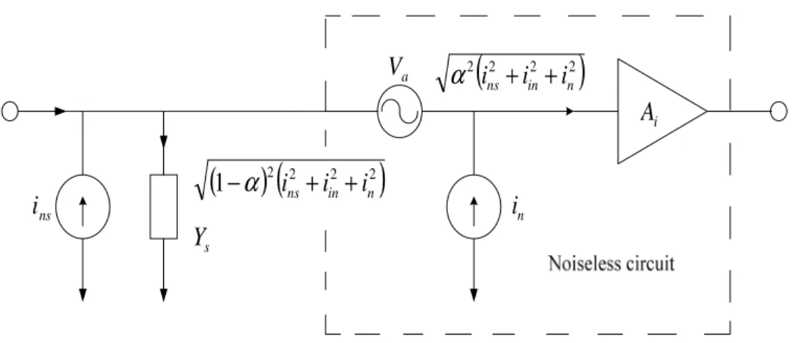
One of the most common ways to test the linearity of a circuit is to apply two signals at the input, having equal amplitude and offset by some frequency, and plot
show in Figure 2-2. From the plot, the third-order intercept point (IP3) is determined. The third-order intercept point is a theoretical point where the amplitudes of the fundamental tones at 2ω1−ω2 and 2ω2−ω1 are equal to the amplitudes of the
fundamental tones at ω and 1 ω . 2
From Table 2.1, if v1 =v2 =vi, then the fundamental is given by
fund= 1 3 3
4
9
i ik
v
v
k
+
(2.28)The linear component of (2.28) given by
fund=
k
1v
i (2.29)can be compared to the third-order intermodulation term given by
IM3= 3 3
4
3
iv
k
(2.30) The small vi, the fundamental rise linearity (20dB/decade) and that the IM3 terms rise as the cube of the input (60dB/decade). A theoretical voltage at which these two tones will be equal can be defined:1
4
3
3 1 3 3 3=
IP IPv
k
v
k
(2.31) This can be solved for vIP3 :1 3
3
2
k
k
v
IP=
(2.32)That (2.32) gives the input voltage at the third-order intercept point. The input power at this point is called the input third-order intercept point (IIP3). If IP3 is specified at the output, it is called the output third-order intercept point (OIP3).
The third-order intercept point cannot actually be measured directly, since by the time the amplifier reached this point, it would be heavily overloaded. Therefore, it is useful to describe a quick way to extrapolate it at a given power level. Assume that a device with power gain G has been measured to have an output power of P1 at the
fundamental frequency and a power of P3 at the IM3 frequency for a given input
power of Pi, as illustrated in Figure 2-2. On a log plot of P3 and P1 versus Pi, the IM3 terms have a slope of 3 and the fundamental terms have a slope of 1. Therefore,
1
3
3
1=
−
−
iP
IIP
P
OIP
(2.33)3
3
3
3=
−
−
iP
IIP
P
OIP
(2.34) since subtracation on a log scale amounts to division of power.Also note that
i
P
P
IIp
OIP
G
=
3
−
3
=
1−
(2.35) These equations can be solved to given[
1 3]
[
1 3]
12
1
2
1
3
P
P
P
G
P
P
P
IIP
=
+
−
−
=
i+
−
(2.36)In addition to measuring the IP3 of a circuit, the 1-dB compression point is another common way to measure linearity. This point is more directly measurable than IP3 and requires only one tone rather than two. The 1-dB compression point is simply the power level, specified at either the input or the output, where the output power is 1dB less than it would have been in an ideally linear device. It is also marked in Figure 2-2. [10]
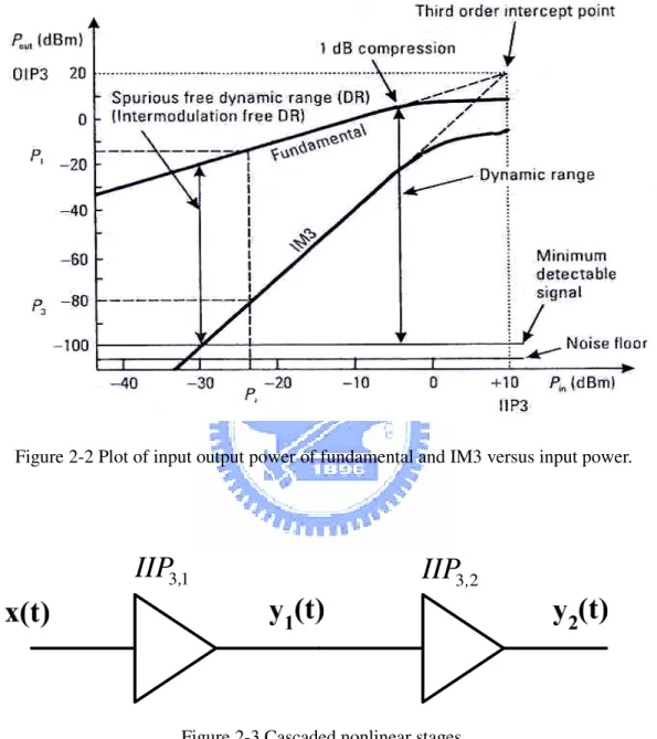
2.2.2 Cascaded Nonlinear Stages
Since in RF systems, signals are processed by cascaded stages, it is important to know how the nonlinearity of each stage is referred to the input of the cascade. Consider two nonlinear stages in cascade. As shown in Figure2-3. Assuming that the input-output relationship is
y
1(
t
)
=
α
1x
(
t
)
+
α
2x
2(
t
)
+
α
3x
3(
t
)
(2.37)(
)
(
)
(
)
3 13(
)
2 1 2 1 1 2t
y
t
y
t
y
t
y
=
β
+
β
+
β
(2.38) Substitute (2.37) into (2.38) results in the relation)
(
)
2
(
)
(
)
(
3 3 3 1 2 2 1 1 3 1 1 2t
x
t
x
t
y
=
α
β
+
α
β
+
α
α
β
+
α
β
(2.39) If we consider only the first- and third-order terms, then3 3 1 2 2 1 1 3 1 1 3
2
3
4
β
α
β
α
α
β
α
β
α
+
+
=
IPA
. (2.40)2 , 3 2 2 1 2 2 1 , 3 2 3 2 1
2
3
1
1
IP IP IPA
A
A
α
β
β
α
+
+
=
, (2.41)where AIP3,1 and AIP3,2 represent the input IP3 points of the first and second stages,
respectively. From the above result, we note that as α increases, the overall IP1 3
decreases. This is because with higher gain in the first stage, the second stage senses larger input levels, thereby producing much greater IM3 products [11].
Table 2.1
Frequency Component Amplitude
dc
(
2)
2 2 1 2 0 2 v v k k + + 1 ω + + 2 2 2 1 1 3 1 1 2 3 4 3 v v v k v k 2 ω + + 2 1 2 2 2 3 2 1 2 3 4 3 v v v k v k 1 2ω 2 2 1 2v k 2 2ω 2 2 2 2v k 2 1 ω ω ± k2v1v2 1 2 ω ω ± k2v1v2 1 3ω 4 3 1 3v k 2 3ω 4 3 2 3v k 2 1 2ω ±ω 2 2 1 3 4 3 v v k 1 2 2ω ± ω 2 2 1 3 4 3 v v k nsi
sY
( )
1
2(
2 2 2)
n in nsi
i
i
+
+
−
α
iA
aV
ni
(
2 2 2)
2 n in nsi
i
i
+
+
α
Figure 2-2 Plot of input output power of fundamental and IM3 versus input power.
1 3,
IIP
IIP
3,2Chapter 3
Basic LNA Design
3.1 Consideration in Low-Noise Amplifiers
3.1.1 Impedance Matching
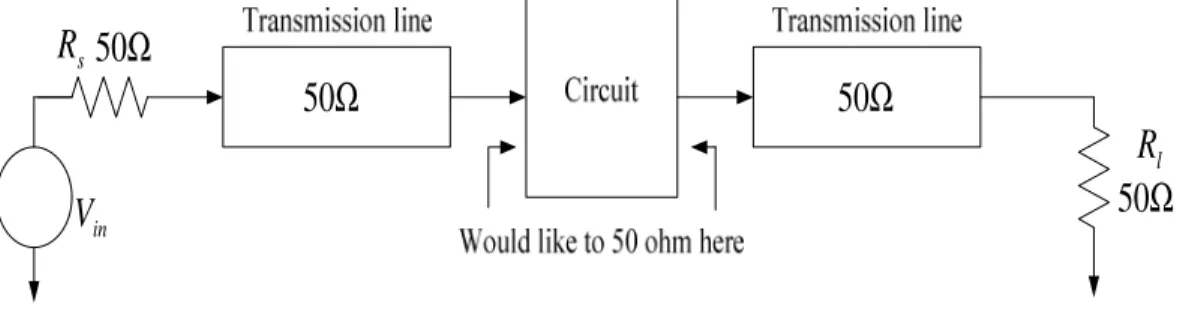
Consider the RF system shown in Figure 3-1. Here the source and load are 5
Typically, reactive matching circuits are used because they are lossless and
because they do not add noise to the circuit will only be matched over a range of
frequencies and not at others. If a broadband matching is required, then other
techniques may need to be used. An example of matching a transistor amplifier with a
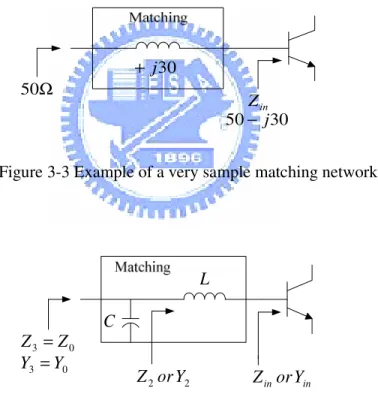
capacitive input is shown in Figure 3-3. The series inductance adds an impedance of
L
jω to cancel the input capacitive impedance. Note that, in general, when an impedance is complex
(
R+ jX)
. Then to match it, the impedance must be driven from its complex conjugate(
R− jX)
.in
Z 5
The input impedance of a circuit can be any values. In order to have the best
power transfer into the circuit, it is necessary to match this impedance to the
impedance of the source driving the circuit. The output impedance must be similarly
matched. It is very common to use reactive components to achieve this impedance
transformation, because they do not absorb any power or add noise. Thus, series or
parallel inductance or capacitance can be added to the circuit to provide an impedance
transformation. Series components will move the impedance along a constant
resistance circle on the Smith Chart. Parallel components will move the admittance
along a constant conductance circle. Table 3.1 summarizes the effect of each
component.
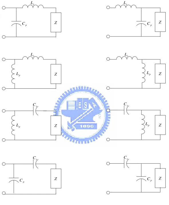
With the proper choice of two reactive components, any impedance can be
moved to a desired point on the Smith Chart. There are eight possible
two-components matching networks, also known as ell networks, as shown in Figure
3-5. Each will have a region in which a match is possible and a region in which a
match is not possible.
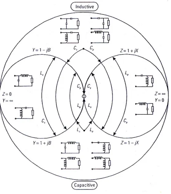
In any particular region on the Smith Chart, several matching circuits will work
networks will work in which regions. Since more than one matching network will
work in any region, how does one choose? There are a number of popular reasons for
choosing one over another.
1. Sometimes matching component can be used as dc blocks (capacitors) or to
provide bias currents (inductors).
2. Some circuits may result in more reasonable component values.
3. Personal preference. Not to be underestimated, sometimes when all paths
look equal, you just have to shoot from the hip and pick one.
4. Stability. Since transistor gain is higher at lower frequencies, there may be a
low-frequency stability problem. In such a case, sometimes a high-pass
network (series capacitor, parallel inductor) at the input may be more stable.
5. Harmonic filtering can be done with a lowpass matching network (series L, parallel C). This may be important, for example, for power amplifiers. [10]
Table 3.1
Component Added Effect Description of Effect
Series inductor z→z+ jωL Move clockwise along a resistance circle
Series capacitor z→z− j ωC Smaller capacitance increases impedance
(
− j ωC)
to move counterclockwise along a conductance circleParallel inductor y → y− j ωL Smaller inductance increases admittance
(
− j ωL)
to move counterclockwise along a conductance circleParallel capacitor y → y+ jωC Move clockwise along a conductance circle
Ω
50
50
Ω
Ω
50
Ω
50
lR
inV
sR
Ω
50
Ω
50
sR
Ω
50
Z
inFigure 3-2 Circuit embedded in a 50 .
30 j + Ω 50 in Z 30 50 j−
Figure 3-3 Example of a very sample matching network.
L
C
0 3Z
Z
=
0 3Y
Y
=
2 2or
Y
Z
Z
inor
Y
ins L Z p C s L Z p L s C Z p L s C Z p C Z p C s L Z Z Z p C s L p L s C p L s C
Figure 3-5 The eight possible impedance-matching networks with two reactive
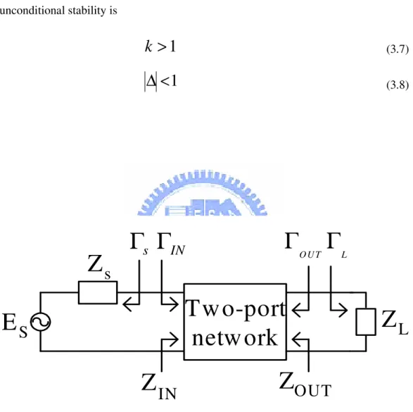
3.1.2 Stability
The stability of an amplifier is a very important consideration in a design and
can be determined from the S parameters, the matching networks, and the
terminations. A two-port network to be unconditionally stable can be derived from
(3.1) to (3.4).
1
<
Γ
s (3.1)1
<
Γ
L (3.2)1
1
22 1 2 2 1 11−
Γ
<
Γ
+
=
Γ
L L N IS
S
S
S
(3.3)1
1
11 1 2 2 1 22−
Γ
<
Γ
+
=
Γ
S s OUTS
S
S
S
(3.4)The two-port network is shown in Figure 3-7. For unconditional stability any passive
load or source in the network must produce a stable condition. The solution of (3.1) to
(3.4) gives the required conditions for the two-port network to be unconditionally
stable. [12] 21 2 1 2 2 2 2 2 11
2
1
S
S
S
S
k
=
−
−
+
∆
(3.5) 21 12 22 11S
S
S
S
−
=
∆
(3.6)A convenient way of expressing the necessary and sufficient conditions for unconditional stability is
1
>
k
(3.7)1
<
∆
(3.8)E
S
Z
s
Γ
s
Γ
IN
Z
IN
Two-port
network
OUTΓ
Γ
LZ
OUT
Z
L
3.2 Wide-band LNA design
Figure 3-8 is the LNA circuit schematic. We discuss this circuit step by step
from the first stage. First, to make1/gm = 50Ω, the gm value of common gate amplifier is going to be fixed at certain trans-conductance. An additional stage is
required to provide sufficient gain over the desired band. A shunt feedback common
source amplifier is used in the second stage for this purpose. The first step is the
selection of transistor size and bias condition of the M1 to yield
Ω = =1/ 50
ReZ11 gm . This ensures input matching condition for wide-band of frequency. But this condition is violated with optimum noise condition. There is a
trade-off between noise and impedance matching in the LNA circuit. One of the major
problems in the wide bandwidth amplifier design is the limitation imposed by the
gain-bandwidth product of the active device. We know that any active device has a
gain roll off at high frequency because of the gate-drain and gate-source capacitance
in the transistor. This effect degrades the forward gain as the frequency increases and
eventually the transistor stops functioning as an amplifier at the high frequency.
Therefore the second design step is the selection of optimal bias point of second stage
of LNA so that it operates at its maximum fT. In addition to this S degradation 21
with frequency other complications that arises in wide-bandwidth amplifier design
feedback configuration is used to reduce these effects and increase the bandwidth. An
inductor L is connected in series with Rf such that after certain frequency the negative
feedback decreases in proportion to the S21 roll-off. This technique improves gain
flatness at high frequency. The load inductance of L1 and L2 replace the resistor load
which is used conventionally. The magnitude of the inductor’s impedance increases as
frequency increases. This increase inductor impedance compensates the active device
gain degradation that occurs at high frequency [13].
Another wide-band LNA design schematic is shown in Figure 3-9. In Figure
3-9, the Rf is added as a shunt feedback element to the conventional cascade narrow
band LNA and Lload is used as shunt peaking inductor at the output. The capacitor Cf
is used for the ac coupling purpose. The source follower, composed of M3 and M4, is
added for measurement proposes only, and provides wideband output matching. C1
and C2 are ac coupling capacitor. The small-signal equivalent circuit at he input of the
LNA is shown in Figure 3-10. The resistor RfM =Rf /(1−Av) represents the Miller equivalent input resistance of Rf, where Av is the open-loop voltage gain of the LNA.
From equivalent circuit, the value of Rf can be much larger than that of the
conventional resistance shunt-feedback. In the conventional resistance shunt-feedback,
the size of Rf is limited as RfM determines the input impedance. One of the key roles of
input circuit. The Q-factor of the circuit shown in Figure 3-10 can be approximately given by gs fM g S T S WB
C
R
L
L
R
Q
⋅
⋅
+
+
≈
0 2 0)
(
1
ω
ω
ω
(3.9) From (3.9), and considering the inversely linear relation between the -3dBbandwidth and the Q-factor, the narrowband LNA in Figure 3-9 can be converted into
a wideband amplifier by the proper selection of Rf. To design a wideband amplifier
that covers a certain frequency band, the narrowband amplifier will be optimized at
the center frequency. The feedback resistor Rf also provides its conventional roles of
flattening the gain over a wider bandwidth of frequency with much smaller noise
E VDD VDD VG1 VG2 M2 M1 50 C1 C2 Cf C3 Rbias Rf Lf L1 L 2 RL
Figure 3-8 Wide-band LNA circuit schematic.
Lg C1R b ias Vg1 Ls Lload Rload M1 M2 M3 M4 C2 Rf Cf IN O U T VD D VD D Vg2
s
T
L
ω
Chapter 4
UWB CMOS LNA Design
4.1 Design Procedures
This circuit is three-stage LNA, Figure 4-1 shows the proposed ultra-wideband
CMOS LNA topology, Figure 4-2 shows the chip layouts. We first use
inductor-resistance feedback to pull the gain at low frequency. So we can reach flat
gain in 3.1 to 10.6 GHz. As the circuit is operated when relatively low frequency, the
impedance of the inductance is low, the amount of inductance-resistance feedback is
strengthened, make gain drop and make circuit relatively stable, and when the circuit
is operated in relatively high frequency, the impedance of the inductance is high, the
amount of inductance-resistance feedback is diminished, gain drops slightly, and
when the inductance in inter-stage heals high frequency, impedance heavy, make
Rout Gm
Av1= 1⋅ becomes great, so after the proper selecting value, will enable reaching flat-gain in operating the frequency band.
Use inductance and inductor-resistance feedback to reach input matching. At
output we use current-buffer to reach matching. Inductive degeneration can be used
and gone to reach simultaneous matching in narrow-band amplifier. The same, can
also be used in Broadband amplifier to reach matching.
over the whole bandwidth is essential. A technique that satisfied this requirement of
large bandwidth at low cost is known as shunt peaking. The resistance Rd improves
the gain at lower frequency. At high frequency, the Ld can improve the gain.
1 L f L f R 1 d L Ld2 1 d R Rd2 s L p C b R 2 L
4.1.1 Inductor-Resistance Feedback
We consider with a parallel low Q LC circuit, as shown in Figure 4-3, and can
write a admittances formula:
2 2 2 2 2 2 2 2
1
1
LP CP(
CP LP)
ab LP LP LP cp LP LP CP CP CP CP LP LPr
X
r
X
Y
j
r
jX
r
jX
r
X
R
X
r
X
r
X
=
+
=
+
+
−
+
−
+
+
+
+
(4.1)When the imaginary part is zero, it indicates that the parallel circuit is at resonance,
and we get 2 2 2 2 CP LP CP CP LP LP
X
X
r
+
X
=
r
+
X
(4.2) There we use cp 1 P X C ω= andωLP = XLP, then (4.2) become
2 2 2
(
)
P P LP P P P P CPL
C r
L C L
C r
ω
=
−
−
(4.3) From (4.3), if we choose P L P C P PL
r
r
C
=
=
(4.4)then the tank circuit should be pure resistance at any frequency.
The Figure 4-4 shows a general common-source amplifier with inductor
1
m1
in S T S gs gs gsg
Z
L
L
sC
C
sC
ω
=
+
≈
+
(4.5)And we consider an inductor-resistor feedback amplifier which is shown at
Figure 4-5, the feedback circuit can be analysis by Miller approximation. It is result
that an equivalent circuit is shown at Figure 4-6, where Lf =
(
L2 Av)
and(
R Av)
Rf = 2 , Av is noted as voltage gain. Figure4-6 is similar to Figure 4-3, if we set Cgs C Lf= P, =LP andrCP=ωT SL . And from (4.4) we can get the formula:
2 2
(
m)
(
) /
S gs m S gs gsg
Lf
L
C
g L
C
C
=
×
=
(4.6) andLf
Av
L
2
=
⋅
(4.7) So, from (4-6) and (4-7), feedback inductor can be decided.[15]dc i p L L= Lp R R= P C C= Cp R R=
Figure 4-3 Parallel resonance circuits.
s
L
in
Z
s L 2 L 2 R
Figure 4-5 A source degeneration amplifier with inductor-resistor feedback.
dc i f L L= f R R= gs C C= gs s gm C L R= ∗
Figure 4-6 The equivalent circuit of source degeneration amplifier with
4.1.2 Shunt Peaking
A model of shunt peaking amplifier is shown in Figure 4-7. The capacitance C
may be taken to represent all the loading on the output node, including that of a
subsequent stage. The resistance R is the effective load resistance at that node and the
inductor provides the bandwidth enhancement. It’s clear from the model that the
transfer function in out
i
v is just the impedance of the RLC network, so it should be straightforward to analyze. The addition of an inductance in series with the load
resistor provides an impedance component that increases with frequency, which helps
offset the decreasing impedance of the capacitance, leaving net impedance that
remains roughly constant over a broader frequency range than that of the original RC
network. The impedance of the RLC network may be written as
(
)
sC
R
sL
s
Z
(
)
=
+
//
1
(4.8) We introduce a factor m, defined as the ratio of the RC and L/R time constant:R
L
RC
m
/
=
(4.9) Then, the transfer function becomes1
)
1
(
1
1
)]
/
(
[
)
(
2 2 2+
+
+
=
+
+
+
=
m
s
m
s
s
R
sRC
LC
s
R
L
s
R
s
Z
τ
τ
τ
(4.10) whereτ
=L/R.2 2 2 2 2
)
(
)
1
(
1
)
(
)
(
m
m
R
j
Z
ωτ
τ
ω
ωτ
ω
+
−
+
=
(4.11) so that)
1
2
(
)
1
2
(
2 2 2 2 1+
+
−
+
+
+
+
−
=
m
m
m
m
m
ω
ω
(4.12)where 1 is the uncompensated -3dB frequency. Chosem=1+ 2 ≈2.414, then can lead to a bandwidth that is about 1.72 times as large as the un-peaked case.
Hence, at least for the shunt-peaked amplifier, both a maximally flat response and a
substantial bandwidth extension can be obtained simultaneously.[9]
V
outC
L
R
i
in4.2 Simulation Results
Figure 4-8 shows the simulated input and output reflection coefficients. S11 is
lower than -10dB between 3.1 and 12GHz. The output buffer achieves excellent
matching such that S22 is lower than -16dB from 3.1GHz to 10.6 GHz. Figure 4-9 is
the power gain versus frequency, and the maximum power gain is 9.27dB in our
simulation results. Since the output source follower drives a matched load, the voltage
gain of the core amplifier is exactly 6dB higher than S21. The -3dB bandwidth is
0.4~9.9GHz for the simulation. The noise figure (NF) of this UWB LNA is shown in
Figure 4-10. The noise figure is as low as 4.12dB at 10.6GHz, while the average noise
figure in-band is about 4.7dB. Figure 4-11 and 4-12 show the simulated reverse
isolation S12 and stability factor respectively. The two-tone test results for third-order
intermodulation distortion are shown in Figure 4-13. The test is performed at 5.5GHz.
IIP3 is to 5.19dBm, and the input referred 1-dB compression point (ICP) is -2dBm.
These results imply excellent linearity of our LNA. The proposed UWB LNA
Figure 4-8 Simulated S11&S22.
Figure 4-10 Simulated NF.
4.3 Measurements and Conclusions
The following Figure4-14 ~ Figure4-19 are the measurement result which are
slightly different from simulation. Which imply good accuracy of simulation and
good circuit design. The some of the gain compression at high frequency showing in
Figure 4-14 maybe due to the underestimate of the load resistor parasitic.
The bandwidth of this work with considering matching and gain is from 2 to 10
GHz, while the average gain is about 7dB. Figure 4-16 shows the measurement result
of S11 and the Figure 4-17 shows the measurement result of S22. Input and output
matching are achieved very well from 2 to 10 GHz. The S11 can bellow -9dB and the
S22 can bellow -16dB. Figure 4-18 shows the measured noise figure. The noise
performance is very flat and the minimum noise figure is 5.97dB at 4GHz. The noise
figure can be better if we solve the resistor parasitic. Figure 4-20 shows the die photo
of this circuit. Total power consumption is 32.7mw which the vdd is 1.8V and vg1 is
0.75v and vg2 is 0.7v. Table 4.1 is the measurement result summary. By the
inductor-resistance feedback we proposed, a good input and output matching,
broadband, a low power consumption amplifier is developed for UWB system
0 2 4 6 8 10 12 14 0 2 4 6 8 10 S 21 (d B ) Frequency(GHZ) Figure 4-14 Measured S21. 0 2 4 6 8 10 12 14 -45 -42 -39 -36 -33 -30 S 12 (d B ) Frequency(GHZ)
Figure 4-15 Measured S12. 0 2 4 6 8 10 12 14 -50 -45 -40 -35 -30 -25 -20 -15 -10 -5 0 S 11 (d B ) Frequency(GHZ) Figure 4-16 Measured S11. 0 2 4 6 8 10 12 14 -30 -27 -24 -21 -18 -15 -12 -9 -6 S 22 (d B ) Frequency(GHZ)
Figure 4-17 Measured S22. 0 2 4 6 8 10 12 14 0 4 8 12 16 20 N F( dB ) Frequency(GHZ)
Figure 4-18 Measured noise figure.
-20 -15 -10 -5 0 5 10 -50 -40 -30 -20 -10 0 OP3 OP1 O ut pu t P ow er (d B ) Intput Power(dB)
Figure 4-19 Measured linearity.
Figure 4-20 Die photo.
B.W.
(GHz)
Gain
(dB)
NF
(dB)
S11
(dB)
S22
(dB)
IIP3
(dBm)
Pdc
(mW)
2~11
7
6.2< -9
< -16
-3
32.7
Chapter 5
Summary
By the inductor-resistance feedback we proposed, a good input and output
matching, broadband, a low power consumption amplifier is developed for UWB
system applications.
Table 5.1 is the comparison of broadband LNA performance.
Ref.
B.W. (GHz) Gain (dB) NF (dB) S11 (dB) S22 (dB) IIP3 (dBm) Pdc (mW) Tech. year[16]
2.4~9.5
9.3
4~9
< -9 < -20 -6.7
9∗.18
CMOS2004
[17]
0.6~22
8.1
4.3~6 < -8 < -9
NA
52
.18
CMOS2003
This
work
2~11
7
6.~6.3 < -9 < -16
-3
32
.18
CMOS2006
Reference
[1] H. S. Momose, F. morifuji, T. Yoshittomi, T Ohguro, M. Saito, T. Morimoto, Y.
Katsuma, H. Iwai, “High frequency AC characteristics of 1.5nm gate oxide
MOSFET ” IEEE international Electron Device Meeting, December 1996.
[2] S. P. Voinigescu, S. W. Tarasewicz, T. MacElwee, and J. Ilowski, ”An assessment
of the state-of-the-art 0.5um bulk CMOS technology for RF applications” proc.
IEEE internationall Electron Devices Meeting, 1995.
[3] J.C. Rudell, J.J. Ou, R. S. Narayanaswami, et al. “Recent development in high
integration multi-standard CMOS transceivers for personal communication
systems” invited paper at the 1998 International Symposium on Low Power
Electronics,1998.
[4] A. Rofougaran, G. Chang, J. Rael, et al. “A single –chip 900MHz spread spectrum
wireless transceiver in 1mm CMOS-part I: architecture and transmitter design.”
[5] J. Rudell, et al.,“A 1.9GHz wide band IF double conversion CMOS receiver for
cordless telephone applications” IEEE J. Solid-state Circuits, vol.32,
pp.2071-2088, Dec.1997.
[6] P. Orsatti, F. Piazza, Q. Huang, and T. Mosrimoto, “A 20 mA receive 55 mA
transmit GSM transceiver in 0.25-mm CMOS,” in In Int. Solid-State Circuits Conf.
Dig. Tech. Papers.(San Francisco), pp. 232-233,Feb. 1999.
[7] C.Yoo and Q.Huang, “A common-gate switched,0.9W class E power with 41%
PAE in 0.2µm CMOS.” In 2000 Symposium on VLSI circuits,(Honolulu,
HI),pp.56-57, June 2000.
[8] P. Miliozzi, K. Kundert , K. Lampaert , P. Good, and M. chian, “A design system
for RFIC: Challenges and solutions.” Proceedings of the IEEE, Oct.2000.
[9] T. H. Lee, The Design of CMOS Radio-Frequency Integrated Circuits, 1st ed. New
York: Cambridge Univ. Press, 1998.
Boston :Artech House,c2003.
[11] B. Razavi, RF Microelectronics, 1st ed. NJ, USA: Prentice-Hall PTR, 1998.
[12] G. Gonzalez, Microwave Transistor Amplifiers Analysis and Design, 2nd ed. NJ:
Prentice-Hall, Inc. 1997.
[13] S. Vishwakarma, S. Jung and Y. Joo, “Ultra Wideband CMOS Low Noise
Amplifier with Active Input Matching,” IEEE Ultra Wideband Systems, 2004.
Joint with Conference on Ultrawideband Systems and Technologies. Joint
UWBST & IWUWBS. 2004 International Workshop on 18-21 May 2004, pp.
415-419.
[14] C-W. Kim, M-S. Kang, P. T. Anh, H-T. Kim and S-G. Lee, “An Ultra-Wideband
CMOS Low Noise Amplifier for 3-5-GHZ UWB System,” IEEE J. Solid-State
Circuits, vol. 40, no. 2, February, 2005.
[15] G-T Lin, “Design of RF CMOS linear Power Amplifier for 802.11a and UWB
Requirements For the Degree of Master of Science In Electronics Engineering,
July 2005.
[16] A. Bevilacqua and A. M. Niknejad, An ultra-wideband CMOS LNA for 3.1 to
10.6 GHz wireless receiver, in IEEE ISSCC Dig. Tech. Papers, 2004, pp.
382 383.
[17] R.-C. Liu, K.-L. Deng, and H.Wang, A 0.6 22 GHz broadband CMOS
distributed amplifier, in Proc. IEEE Radio Frequency Integrated Circuits (RFIC)