Novel Regenerative Sustain Driver for Plasma Display Panel
Song-Yi Lin, Chem-Lin Chen, Kelvin
Lee
Department
of
Electrical Engineering
National Taiwan University
Taipei, Taiwan 10764
Abstract
A novel sustain driver is proposed to drive a plasma display panel(PDP) while minimizing circuit complexity compared with prior approaches. The presented driver uses an inductor to resonate with the equivalent intrinsic capacitance of PDP
so
that the abrupt charging/discharging operation is avoided. The energy loss due to conventional hard switching driving is mainly recovered. All active switches are operated with zero voltage switching and all diodes are turned off naturally without the problem of reverse recovery.Introduction
Plasma display panel(PDP), invented at the university of Illinois in 1964 by Professors Bitzer and Slottow, is known for its wide screen size and thin structure. It has advantages over conventional display technologies by screen size, thinness, durability and wide viewing angle. It is promising that PDPs will soon achieve the goal of consumer affordable hang-on- the-wall color TVs with diagonals ranged from 20 to
60 inches.
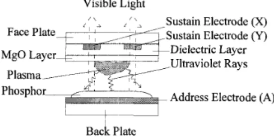
Shown in Fig. 1 is a commonly adopted structure of PDP. It consists of two glass plates with chemically stable rare gases filled between them. The inner space of the PDP panel is divided into numerous local cells by the opaque electrode grid lines encrusted on the inner surfaces of glass plates. Shown in Fig.2 is the illustration of the lighting mechanism for one individual cell. The operating principle, as that of fluorescent lamps, is to utilize gas discharge generated ultraviolet ray to excite a visible light emitting phosphor. -n Dielectric Layei I _._.___._
/
Faceplate3
&
)
/
/ / / L-/
/&tam Elecuode(X) L M ~ O Layei , -Address Electrode Visible Light " Sustain Electrode (X)Face Plate *Sustain Electrode (Y)
P l a s m a - - - d y - y
I , / I
MgO Layer+--
fa dielectric
Layer1
&&p-'
Ultraviolet RaysAddress Electrode (A)
Phospho
Back €"late
Fig.2 Illustration for lighting mechanism of PDP
Despite the gas dischiarge characteristic, PDPs are shown to have inherent capacitance during voltage transients[l]. Shown in Fig.3 is the equivalent model for PDP accompanied with its simplest driver to generate AC driving voltage. For the driving voltage not high enough to cauije gas discharge, the PDP behaves as a capacitor. Once the voltage is high enough to cause discharge, the equivalent capacitance will increase somewhat[2]and the PDP will sink periodical discharge current pulses and there will be light emitted.
Referring to Fig.3, it is verified that during charging or discharging transients of PDP, there is always an amount of energy CV2/2 dissipated in the non-ideal resistance of the wire and channels of MOSFETs. Let f be the operating frequency, then the total power loss is 4*frCV2/2. For driving a large size PDP with large panel capacitance in high frequency high voltage application, this energy loss will increase the demand of power supply and toughen thermal design. Further, the surge chargingldischarging current will cause large amount of EM1 noise which may degrade the circuit performance. The surge current ratings of the controlled switches are also increased.
&-
Fig. 1 Simplified structure of a 3-electrode type AC-PDP
To solve the aforementioned problem, prior approaches[3, 41 as illustrated in Fig.4 and Fig.5 is used. These circuits utilize the resonance between the external inductor and PDP to avoid abrupt chargingldischarging current and thus save large amount of energy. The price paid is the circuit complexity and there will be switching losses on the additional switches.
v v
m A
Fig.4 Prior approach 1
i
-
i
F
l
I I
U U
Fig.5 Prior approach 2
In this paper, a new driver for PDP is proposed. It has very simple structure and possess the same function as that of the prior approaches shown in Fig.4 and Fig.5.
Proposed Circuit
Shown in Fig.6 is the proposed driver for PDPs. It consists of four MOSFETs, MI-M4, and a LC pair connected between the two legs of the full bridge circuit. D1-D4 and Cl-C4 are parasitic components of MOSFETs. The driving signals of the four MOSFETs are the same as that of phase-shifted zero- voltage-switching full-bridge(ZVS-FB) converters. There are specified non-conducting intervals between the conducting periods of M1 and M2 or M3 and M4. The current stored in the inductor is utilized at these intervals to charge/discharge the equivalent capacitance of PDP and MOSFETs and hence soft transient is achieved. Cb is used to block DC current component through the inductor. For Cb large enough, the voltage across it is negligible so that Cb could be simply viewed as a shorted jumper. Detailed circuit operations are presented in the next section.
Circuit Operations
Shown in Fig.7 are the detailed operating waveforms of the proposed driver. Gl-G4 are the respective driving signals of Ml-M4. Circuit operations are divided into two half cycles, tO-t3 and
t4-t7.
explained as followed:
Operating principles of the frst half cycle are
V
?
Fig.6 Proposed driving circuit
t b ~ t 2 ~ t k ~ t 6 ~ t l t3 t5 t7
Fig.7 Operating waveforms of the proposed driver 1)Before to:
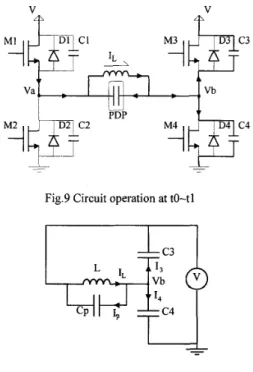
The current path is indicated by the bold line in Fig.8. Vab, voltage across PDP, equals to V and the inductor current increases linearly with slope V L . Assume that the inductor current I, equals to I, at to.
M1 and M4 are conducting.
V V
+
V
?
Fig.9 Circuit operation at to-tl
3
Fig. 10 Equivalent circuit for Fig.9
2)to-t 1 :
At to, M4 is turned off and the inductor current continues to flow through C3, C4 and PDP, as indicated by the bold line in Fig.9. Resonance takes place and the equivalent circuit is shown in Fig. 10 with the equation below:
I,
( t ) = C &
( t ) - V ) ' l ) I , ( t ) = C , V , I))(([ I , ( t ) = C , (V, ( t ) - V > ( l )v - V , < t ) = L I ,
( t ) ' ] ) = L ( I , ( t ) + I , ( [ ) + I , ( t ) P (1)= L ( C 3
+e,
+e,
)V,(t)','
L ( C ,
+e,
+c,
)V, ( t ) ' , ) + V ,( t )
=v
I / , ( O ) = O
(2) I ,(0)
=I,
Rewriting Eq.1 along with its initial conditions, we get
The solution of Eq.2 is
(3)
r
.
vb(t)
= V-Vcos(wt)+-J-sin(wt) 1E
whereC,
=C,
+
C,
+
C,
and w =-
When Vb reaches V, D3 starts to conduct and resonance stops. M3 is tumed on with zero voltage switching after the conduction of D3 since the drain-to- source voltage of M3 is zero prior to its turn-on
JLC,"
command. Substituting: Vb(td)=V into Eq.3, we get
tan(wt, ) = -
-
(4)10
vE
where td, which equals to tl-to, is the time interval for Vb to transit from zero to V.
3)t 1 -t2:
After t l , D3 is conducting and the inductor current circulates through MI and D3. M3 can be tumed on after t l with zero voltage switching since the drain-to- source voltage of M3 is zero. Substituting Eq.4 into Eq. 1, we get
I,
( f d>=I,
( f d ) + I 4 ( l d) + I p
( f d )Since there is no voltage difference through the current loop, the inductor current is kept at a constant magnitude presented in Eq.5.
V
?
Fig. 1 1 Circuit operation at t2-t3
P
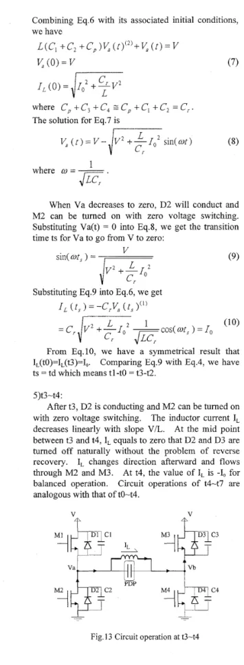
Fig. 12 Equivalent circuit for Fig.11 4)t2-t3:
At t2, M1 is turned off and the inductor current continues to flow through C1, C2 and PDP. Resonance starts again with the equivalent circuit shown in Fig.12. Equations describing this circuit are shown below:
r,
( t )
=c,(v-v,
( t ) ) " )I,
( t ) =-c,v,
(t)'"
I,
( t ) =-e,
(I/ -v,
(t):,'" ( 6 )V ,
( t1-
v
=L
(I,
( t>+
I,
( t )+ I , ( t >>(I) = - L ( C ,+c,
+C,)V, (t)','Combining Eq.6 with its associated initial conditions, we have
L
(C,
+
c,
+ C,
)v,
( p +
v,
( t )
=v
v,
(0)
=v
(7)where
C,
+
C3+ C,
GC,
+
C,
+
C,
=C,.
The solution for Eq.7 is
I
1
where
w
=-
.iLc,'
When Va decreases to zero, D2 will conduct and M2 can be turned on with zero voltage switching. Substituting Va(t) = 0 into Eq.8, we get the transition time ts for Va to go from V to zero:
(9)
V
sin( ut, ) =
j
q
Substituting Eq.9 into Eq.6, we get
I,
( f, ) = -C,V, ( t , ) ( I )From Eq.10, we have a symmetrical result that Comparing Eq.9 with Eq.4, we have IL(t0)=IL(t3)=I,.
ts = td which means tl-tO = t3-t2. 5)t3-t4:
After t3, D2 is conducting and M2 can be turned on with zero voltage switching. The inductor current I, decreases linearly with slope V/L. At the mid point between t3 and t4, I, equals to zero that D2 and D3 are turned off naturally without the problem of reverse recovery. I, changes direction afterward and flows through M2 and M3. At t4, the value of I, is -I, for balanced operation. Circuit operations of t4-t7 are analogous with that of tO-t4.
V V
Design Considerations
Referring to Fig.7, the magnitude of In is determined by
(1 1) V
1,
- f 3 )Rewriting Eq.4, we have
Combining Eq. 1 1 with Eq. 12, we have
-
For practical applications, the DC bus voltage V, which is determined by the firing voltage of the panel, is known. The panel capacitance, Cp, can be measured so that Cr is known also. Once the switching frequency of the system is determined, the interval tl-tO or t4-t3 can be roughly fixed. The parameter left to be determined is the value of L and hence I,.
When using Eq.13 to solve for L, one restriction must be added or there will be numerous solutions. Once L is determined, we can use Eq. 1 1 together with Eq.5 to calculate the maximum current through the inductor.
m 2
Experimental Results
Shown in Fig.14 is the power stage of the experiment circuit with its associated parameters. The plasma display panel under test is 3-inch in diagonal. Sustain electrodes (X) are shorted together and connected to Vb. Sustain electrodes (Y) are shorted together and connected to Va. Shown in Fig.15 are the gate-to-source voltage of Ml-M4 derived from a phase-shifted PWM control IC, UC 3875.
Shown in Fig. 16 are the experiment results without the inductor, severe ringings are observed. When the inductor is applied, soft voltage and current transients are observed as shown in Fig. 17 in which the DC bus is not high enough to cause gas discharge and hence there is no light emitted. For the case shown in Fig.18, there is light emitted and a second current peak due to gas discharge is detected.
s
Sustain electrode (3')Fig. 13 Circuit operation at t3-t4
Fig. 15 Experimental waveforms of Vgsl-Vgs4
Fig. 16 Experimental results without the inductor DC bus equals to 150V, no light emitted
I
_-
I
1P
2 m w
Fig. 17 DC bus equals to 150V, no light emitted
i
I2 m , v
gas discharge wrrent
Discussions
The interval to-tl or t4-t5 is identical to leading leg transition for phase-shifted zero-voltage-switching full-bridge(ZVS-FB) DC-I>C converters[5] while t2-t3 or t6-t7 is identical to lagging leg transition. In ZVS- FB DC-DC converters, the energy stored in the leakage inductor after leading leg transition decreases somewhat depending on the loading condition and it is possible that the stored energy is not enough to achieve ZVS for lagging leg transition. While in the proposed circuit, despite the initial value of I, at to, the stored energy increases after leading leg operation so that ZVS condition for lagging leg operation is always guaranteed. This can be approved because Eq.4 and Eq.9 are always solvable. Additionally, in ZVS-FB DC-DC converters, the time interval of leading leg transition is always shorter than that of lagging leg transition. While in the proposed circuit, these two intervals are identical because of the result obtained from Eq. 10.
Conclusion
Comparing with prior approaches, the proposed sustain driver shown in Fig.6 is quite simple while achieving the same function of efficient driving and soft transients. All active switches are operated with zero voltage switching and all diodes are tumed off naturally without the problem of reverse recovery. The presented circuit is experimentally verified on a 3- inch plasma display panel.
References
[ I ]
Yasutaka Inanaga, Akihiko Iwata, Masaaki Tanaka, “Measurement of wall charges in a surface Discharge AC-PDP’, Proceedings of the Fourth Intemational Display Workshops, pp ,527-530, November, 1997.[2]
Larry F. Weber, “Measurement of wall charge and capacitance variation for a single cell in AC plasma display panel”, IEEE Trans. on Electron Devices, Vol.[3]
Larry F. Weber, Kevin W. Warren, ”Power efficient sustain drivers and address drivers for plasma panel”, U.S . Patent, Number 4,866,349, September, 1989.
[4]
Akio Tanaka, “Low power driver circuit for AC plasma display panel”, U. S . Patent, Number 5,438,290, August,1995.