A
Low Power 2-D DCT Chip Design Using
Direct 2-D Algorithm
Liang-Gee Chen, Juing-Ying Jiu, Hao-Chieh Chang, Yung-Pin Lee,
and
Chung-Wei Ku
DSP/IC Design Lab, Department of Electrical EngineeringNational Taiwan University Taipei, Taiwan, R.O.C. Tel: 886-2-363-5251 ext 332
Fax: 886-2-363-8247
e-mail: {lgchen, howard}Qvideo.ee.ntu.edu.tw
Abstract- In this paper, a low power 8 x 8 2-D DCT
architecture based on direct 2-D approach is proposed. The direct 2-D consideration reduces computational complexity. According to this algorithm, a parallel distributed arithmetic (DA) architecture at reduced supply voltage is derived. In the real circuit imple-
mentation of the chip, a hybrid-architecture adder of
low power consumption is designed, as well as a power-
saving ROM and a low voltage two-port SRAM with sequential access. The resultant 2-D DCT chip is real-
ized by 0.6 pm single-poly double-metal techlnology.
Critical path simulation indicates a maximum input rate of 133MHz, and it consumes 138mW at 100MHz.
I. INTRODUCTION
The Discrete Cosine Transform (DCT), among various transforms, is the most popular and effective one in image and video compression, such as J P E G , MPEG, H.261 and H.263. Since these standards recently apply to battery op- erated systems like portable computers (Notebook), per- sonal digital assistants (PDA) and wireless communica- tion equipments, it becomes imperative t o develop low power DCT chip as one component of these energy-crucial desktops.
Since DCT has been standardized in recent years, many researchers and companies have took lots of resources to implement it. The conventional row-column approach has the advantage of regularity for VLSI implementation, which causes most 2-D DCT chips to be designed in this way. However, the computational complexity of the row- column approach is more than that of the direct method. And low computational amount is considered mainly in low power algorithm level. Although the direct method incurs the irregularity in realizing 2-D DCT chips, the feature of low computational complexity is still attractive for low power DCT chip design. This fact motivates our research for fewer computations and regular 2-D DCT ar- chitecture for real chip implementation with the direct
method.
As to low power DCT design, T. Kuroda et a1.[3] pro- posed a 0.9V, 150MHz, iOmW, 2-D DCT with variable threshold-voltage scheme implemented by 0.3pm CMOS triple-well technology. However, the chip achieved low power by only taking the circuit and device level into ac- count, not including algorithm level consideration. There- fore, we propose a 2-D DCT chip incorporating low power considerations in algorithm, architecture, and circuit de- sign levels.
The paper is organized as follows. In Section 11, the direct 2-D DCT algorithm is briefly discussed. The archi- tecture exploiting this algorithm is decribed in Section 111. In Section IV, The main circuit module designs, including adders and memories, are presented. The core character- istics are shown in Section V. Finally, a conclusion is given in Section VI.
11.
THE DIRECT
2-D D C T A L G O R I T H MThe 2-D DCT of an N x N real signal z ~ , , ~ , , with kernel factor 2 c ( n l ) c ( n ~ ) / N neglected, is defined as
n l = 0 n z = O
q 2 n l + l ) k l ] cos
[
27r(2n2+
l)k2cos
[
4 N 4 N
n l , n z , k l , k z = O , l , . - . , N - 1,
In the following, assume that N is t o be a power of 2.
Thus, Y k l , k 2 can be rewritten as:
N-1 N - l
Now consider the following expression:
n1=0 n2=O
It is not difficult to find that Y k l , k 2 can be computed from
U k l , k 2 by the following set of expressions:
1
Y k 1 , k z -[Re(Ukl,k2) 2 - 1m(UN-k1,k2)1,
Yk1,N-k2 '[-Im(Uki,k,) 2 - Re(UN-kl,kz)]. (4)
Note that (4) requires U k l , k 2 in (3) t o be computed for all
k1 and only a sufficient subset of k2 such that {k2, N - kz} covers all possible values of k 2 .
By the following relation [4]
4722
+
1 = (4t+
1)(4n1+ 1) mod 4N, (5) where 05
t , n 1 , n 25
N - 1, the signal ynl,na is mapped as ynl,t.If
n 1 is fixed, the mapping from n 2 tot
is one-to-one. However, with different nl, the mapping order is not the same.
By substituting (5) into (3), (3) can be rewritten as:
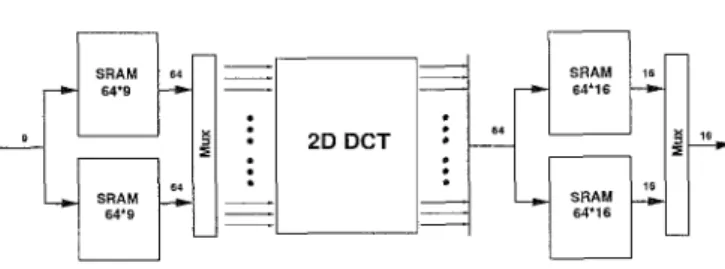
Fig. 1. Low power 2D-DCT whole chip architecture.
Although U j b is a complex number, its real part is in- deed an N-pbint 1-D DCT, and its imaginary part can be obtained by Im{U{,o} = 0, and
This reveals that can be achieved by calculating N-point 1-D DCT. Since multiplying ( - j ) a does not need
any multiplication, but only affects the addition, an N x
N
2-D DCT can therefore be realized by N N-point 1-D D- CT's with some additions. Besides, comparing with the row-column method which needs 2N N-point 1-D DC-T's to perform an N x N 2-D DCT, this approach with less operation complexity is more suitable for low power considerations in the algorithm level.
111.
Low
POWER 2-D D C T ARCHITECTURE Since the direct 2-D DCT algorithm discussed above reduces the computation complexity, it is obvious that an architecture based on it shall lead t o the goal of low pow- er. By reviewing (4) and(&),
the computation from the input zn1,,2 to the output Ynl,n2 is shown in the follow-N-1 N-1 ing.
nl=O t = O
(4n 1 t 1)[k 1 t (4t+ 1) k 2)
(6a) In our computation, first comes the d a t a mapping from
znl,n2 to ynl,t. Then, is obtained by calculating the
1-D complex DCT of y n l , t . Before the final output Y k l , k 2 is finished by (4), U k l , k 2 is computed by the summation with respect to
t
depicted in (6c).After the direct 2-D DCT algorithm is discussed, it is time t o depict the whole low power 2-D DCT chip ar- chitecture shown in Figure 1. Since the DCT input and (6b)
1
N-1 N-1 (4n 1 t 1)[k1+ ( 4 t t 1)kaI2
[E0Yn1ptw4N.
(6c)1
N-1 N-1 ( 4n 1+
1) bc(-j)"
[
Ynl,tW4N t = O nl=OIn the above dudection, we let IC1
+
(4t+
1)kz = a N+
b, where a E integer and 0
5
b5
N - 1. Let the computation of nl's summation be represented by Then we can findN-I
nl=O
output is ranging from -255-255 and -2040-2040, respec- tively, the wordlength of the input data is %bit and that of the output data is 12-bit. However, for convenience, the kernel factor 2c(nl)c(nz)/N is neglected in deducing the direct 2-D DCT method. Therefore, the wordlength of the output data turns out to be 16-bit for covering all the ouput range. Besides, since the 1-D DCT computa- tion is implemented with DA method, two-port SRAMs operating in ping-pong mode are employed for re-ordering the input and output data. Hence, 9-bit input d a t a are fed word-serially and through the input SRAM, the data are converted into 64 bit-serial d a t a for 2-D DCT. Af- ter these data are processed, the output SRAM changes
1 1 : o 1 : : o , - 0 1 : 2 I ! I 0 : 10 1 0 : 3 2 : 1 1 : j o 1 1 ; 4 2 1 2 0 : : 2 0 0 : 5 3 ! 2 1 : ; 2 0 1 : (t) (a) : o 0 1 : 1 3 : o 3 : : o 2 1 : u3.4.5.6,5 - o .... i.! ~ ... , , . 2 2 : 1 1 : : I 0 1 : 3 0 j l 3 ; 11 2 1 ; 4 3 j 2 1 : : 2 0 1 : 5 1 : 2 3 : ! 2 2 1 : 6 0 ! 3 1 : ! 3 0 I /
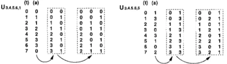
Fig. 2. The 'a' value for U 3 . 4 . 5 . ~ , 1 and U 3 , 4 . 5 . ~ , 5 deduction
* \
\
represents the subtrahend in the subtration. Moreover, the arrangement of the
a
value for u3.4.5.6,5 network d-eduction is also shown in Figure 2 as another example. Furthermore, the final architecture of u3.4.5.6,1 combined
with t h a t of u3.4.5.6,5 is shown in Figure 3, too.
Just as the depiction of (4), there is no necessity for processing the whole set IC1,ICz. In order to complete all Y k 1 , k Z r it takes efforts to compute u k 1 , k z for all IC1 and
only a subset of k z , where kz is 0, 1, 2, 4, 5 in our design.
So far, the bufferfly-like adder/subtracter tree for com- puting U k l , k P are presented. Since our goal is t o design a
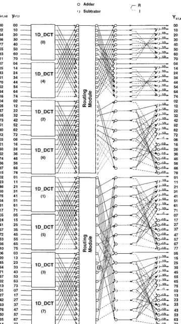
low power 2-D DCT chip a t reduced supply voltage, a par- allel architecture is needed t o compensate for the speed loss due t o lowering operating voltage. Hence, combining the bufferfly-like adder/subtracter tree and the 1-D DCT computation with DA method in parallel form realizes the core of the 2-D DCT chip shown in Figure 4. After t h a t ,
U k l , k Z with IC1 = 0, 1, 2, 4, 5 are obtained and all Y k 1 , k Z
are solved with these values by another adder/subtracter stage according to (4).
IV. CHIP IMPLEMENTATION
Fig. 3. The example for U 3 . 4 . 5 . 6 , 1 and U 3 . 4 . 5 . ~ , 5 architecture deduction
the 64 word-paralell d a t a t o 16 bit-paralell d a t a for next stage, usually zig-zag scan.
In order to deduce the architecture which processes the d a t a from t o u k l , k 2 , it is found after a deep investiga-
tion that each U k 1 , k z can be gained through a butterfly-
like adder/subtracter network, which is constructed by re-arranging the value a in summation of ( - j ) = shown in
Take the network deduction of U k l , k P where IC1 = 3, 4,
5, 6; IC2 = 1, 5 for example. Figure 2 shows the deduction
process. In computing u k l , l shown in (6c), as the sum-
mation index
t
goes from 0 to 7, the exponential valuea
of (-j) changes to 0 , 1 , 1 , 2 , 2 , 3 , 3 , 0 in sequence. Since adding 1 t o a means a rotation by 90 degree, the originala values can be divided into several segments for seeking some general rules. Therefore, as shown in the left side of Figure 2, the a values for computing U k l , l are divid-
ed into 3 segments. Note t h a t the sum of each row in the dashed box is either equal t o the original a value, or led/trailed by 360 degree. Besides, the three segments of
a value mean t h a t there will be an adder tree of three-
stage to complete the simulation with index
t
from 0 to 7.After analyzing the three segments of a values, it is not difficult t o find t h a t the summation with respect to
t
can be also separated into two groups: one is the even values o f t , and the other is the odd values o f t .According to the segmentation of a value and the group- ing o f t , the final network configuration for calculating
u k l , l for k l = 3 to 6 is shown in Figure 3. The dash-line
(6c).
The proposed low power 2-D DCT chip consists of mainly adders, memories and registers. Thus, reducing the power consumption in these components will make more contribution to achieve low power.
A. Adder Design
The adder is used as the accumulator in calculating the 1-D DCT result. Since the adder is also operating a t low voltage, the parallelism is employed in order t o com- pensate for the speed loss. First, the adder adopts the square-root carry-select structure shown in Figure 5 for its propagation delay is proportional to
f l .
After di- viding the larger adder into several stages, the stages are implemented with Manchester adder for its improvement on the carry-lookahead by using a single gate for gener- ating carryCi.
Therefore, a large-bit adder is formed by combining the square-root carry-select adder in architec- ture and Manchester adder in stage circuits. This adder has two characteristics inherited from the two adders men- tioned above: carry-select for high speed and Manchester for low power.B. Power-Saving ROM
Since the 1-D DCT in our chip is implemented by DA method, the ROM is needed t o hold the content of the look-up table which is pre-computed. In order to elimi- nate the static power consumption due to the DC path existing in static pseudo-nMOS ROM, a better approach is to use precharged logic. The ROM decoder and d a t a cir- cuits are shown in Figure 6. An address transition detec- tion (ATD) circuit is employed t o generate the prechrage
xni,n2 00 22 44 66 77 55 33 11 07 25 43 61 70 52 34 16 04 26 47 65 73 51 30 12 03 21 40 62 74 56 37 15 02 23 46 60 75 54 31 17 05 24 41 67 72 53 36 10 06 20 45 64 71 57 32 13 01 27 42 63 76 50 35 14 I - R 0 Adder [ J Subtrator 1 Y k 1 . e M) 10 20 30 40 50 60 70 04 14 24 34 44 54 64 74
Fig. 4. The proposed parallel DA 2-D DCT architecture
signal p r e , which is activated only when the input address-
es change. The ROM decoder and d a t a circuits are shown in Figure 6. During the precharge phase, p r e = 0 and the bit-lines are precharged to Vbo. Meanwhile, the AND gates in decoder ensure t h a t all pull-down paths through the NMOS are off during precharging. In the evaluation phase, pre = 1 and if the word-line is activated high, the bit-line is discharged. For the PMOS and NMOS are not turned on simultaneously during precharging or evalua- tion phase, there is no DC path from V D ~ to G N D , and thus, no static DC power dissipation.
C. Low-Voltage Two-Port S R A M
Since the proposed 2-D DCT is implemented with DA parallel architecture, the d a t a reordering is needed for bit-serial word-parallel d a t a operation. Thus, the two-
Carry1 Carry0 Carry 1 Carry 0
carry1 carry0
I I
I I
t
t
t
t
MUX MUX MUX MUX
CI
t
t
t
t
MUX MUX MUX MUX
CI
Fig. 5. The architecture of the high-speed low-power adder
V VDD ord 11”. GND GND It 11“. ulput latch DO D1 0 2 03 PlS
Fig. 6. ROM decoder a n d ROM data Circuit in the proposed power-saving ROM
port SRAM shown in Figure 7 is used for d a t a mapping and d a t a reordering. Note that the input port size n is different from the output port size m. While the twc- port SRAM (n = 9,m = 64) is for the input ping-pong mode, the (n = 64,m = 16) two-port SRAM is for the ouput ping-pong mode. The sense amplifier consists of a cross-coupled pair of PMOS transistors and NMOS input devices. This differential pair applies the positive feed- back t o accelerate the sense speed.
D. The Register
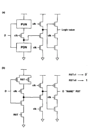
Since the single clocking strategy is adopted in our de- sign, the TSPC D F F is used for simplicity and its low transistor-count. After the original T S P C DFF[5] struc- ture is re-examined, the pull-up network (PUN) and the pull-down network (PDN) are recognized from the first stage of this structure. They are shown in Figure 8(a). Hence the logic function can be put into the P U N - and PDN-network complementarily. For example, assume a NAND gate is to be combined with the T S P C DFF. The PUN consists of two parallel PMOS transistors and the PDN is composed of two series NMOS transistors. Thus, the T S P C D F F including NAND logic is shown as Fig- ure 8(b) and the additional iuput is used for reset signal
Fig. 7. The core of the two-port SRAM circuits including memory cells, write buffers, sense amplifiers, and precharging circuits
TABLE I
Chip Characteristics Internal Wordlength 16 bits
Technology 0.6pm CMOS SPDM No. of Transistors 152017 Core Size 7.85mmx6.45mm Die Sine 8 . 9 8 m m X 7.79" ~ Clock Rate 100 MHz Latency 198 cycles Block size 8 x 8 Supply Voltage 2.0
v
Power 138 m Wsequential addresser in SRAM and counters for their logic function. And they have better performance in power and speed than that of static CMOS DFFs for less transistor- count.
V. CHIP PERFORMANCE A N D SPECIFICATIONS
By incorporating the module circuits discussed above, the proposed low power 2-D DCT chip with direct method is implemented. Figure 9 shows the photomicrograph of the whole system chip. The core characteristics are sum- marized in Table I.
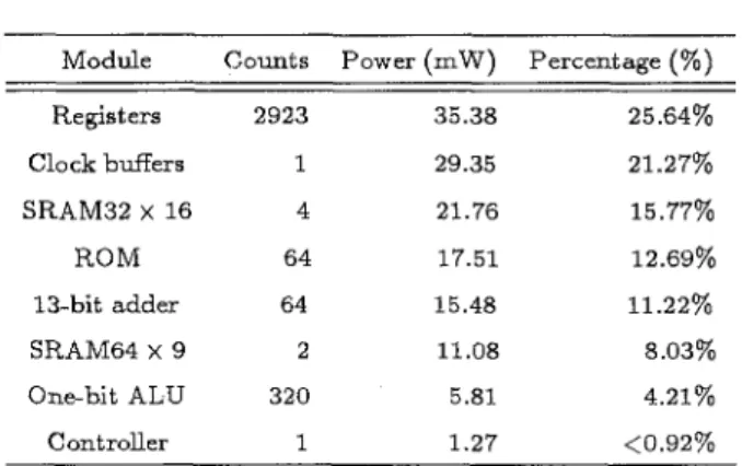
Besides, in order t o understand more details about the power distribution in the designed chip, a power simu- lation a t 100 MHa by components is shown in Table 11.
From this table, it is obvious that registers consume most
Logic value D - RST-1
-
D RST=O-
1 "NAND" R S lFig. 8. (a) TSPC Register including logic tree (b) TSPC Register including NAND logic
power than others do. Then, excluding the clock buffers, the first runner up is memory modules. Hence, reduc- ing the power consumption of registers and memories will contribute more t o achieve the proposed chip. That is the reason why we design low power components such as registers, memories and adders.
Since the DCT is applied t o portable applications re- cently, the power consumption becomes a critical point in designing a 2-D
DCT
chip. The implementation in [l] and the product presented in [2] are not dedicated to low pow- er design. Thus, they consumes larger power. The chip reported by [3] which utilized variable threshold-voltage scheme by controlling back-bias voltage and better tech- nology achieved a lOmW 2-D DCT core processor. The main features of these chip implementation are summa- rized in Table 111.Although the chip presented by [3] consumes low pow- er, its implementation lacks the low power consideration in algorithm level. Our chip is design by taking the low power algorithm, architecture, and circuits into consider- ation. The ideas in both chips do not conflict. Hence, combining the low power algorithm and architecture in our chip and the variable threshold-voltage scheme in [3] will lead to a 2-D DCT chip with lower power dissipation than both two chips.
VI. CONCLUSION
A low-power high-performance 2-D DCT chip is im- plemented. The design features that contributes most t o
TABLE I11
Processor Comparison
Authors
D. Slawecki et al. [l]
SGS-THOMSON (21
Tech. Core area Trans. Voltage Clock rate Power 2pm 72.68 mm2 67929 ~ 5 V 5 0 M H z 1 W
- -- 5 v 20 MHz 1.5 W
I
T. Kuroda et al. [3]I
0.3pmI
4 mm2I
120000I
0.9 VI
150 MHzI
10 m WI
our
chip1
0.6pm 50.6 mm2I
152017I
2 V 100 MHz 138mWTABLE I1
Simulated Power Dissipation by Components
Module Counts Power (mW) Percentage (%)
Registers 2923 35.38 25.64% Clock buffers 1 29.35 21.27% SRAM32 x 16 4 21.76 15.77% ROM 64 17.51 12.69% 13-bit adder 64 15.48 11.22% SRAM64 x 9 2 11.08 8.03% One-bit ALU 320 5.81 4.21% Controller 1 1.27 <0.92% technology.
Fig. 9. The photomicrograph of the whole chip including 1/0 pads
REFERENCES
this result are as follows. First, the usage of the direct 2-D DCT algorithm reduces the 2-D DCT into 1-D DCT and some additions. Also, a fast algorithm of 1-D DCT is employed. Both of these decrease the computation- al complexity which means low power consumption per block operation. Besides, a parallel distributed arithmetic (DA) architecture with the direct 2-D DCT approach is proposed in order t o compensate the speed loss due to the reduced internal supply voltage.
In addition to the considerations in algorithm and ar- chitecture level, low power design methdologies in logic- style and circuit level are applied t o the real circuit imple- mentation of the proposed 2-D DCT. Since adders, mem- ories and registers are the main modules of the proposed DCT design, a power-saving in these circuits contribute to the goal significantly.
Finally, the proposed low power 2-D DCT chip with direct method is implemented. The maximum frequency simulated of the chip is 133MHz a t last. It meets the re- quirement of the real-time HDTV signal processing for the chrominance format 4:2:0 and 4:2:2. The power simulated is 138mW a t 100MHz by 0.6 p m single-poly double-metal
[l] D. Slawecki and W. Li,“DCT/IDCT processor design for high data rate image coding,” IEEE Trans. Cir- cuits S y s t . Video Technol., vol. 2, pp. 135-146, June
1992.
[2] SGS-THOMSON Microelectronics, “2-D Discrete Cosine Transform Image Processor,’’ product num.
IMSA 121.
[3] T. Kuroda et al., “A 0.9V, 150 MHz, lO-mV, 4 m m 2 , 2-D Discrete Cosine Transform Core Processor with Variable Threshold-Voltage (VT) Scheme.”, IEEE J .
Solid-state Circuit, vol. 31, no. 11, pp. 1770-1779,
Nov 1996.
[4] Y . P. Lee, T. H. Chen, L. G. Chen, M. J . Chen, and
C . W. Ku, “A Cost-Effective Architecture for 8 x 8 2-
D
DCT/IDCT Using Direct Method”, IEEE T r a n s . Circuits S y s t . V i d e o TechnoE.,vol7. no 3, pp. 459-467, June 1997.[5] J. Yuan and Svensson C.,“High-Speed CMOS Cir- cuit Technique,” IEEE J . Solid-State Circuits, vol24,