www.rsc.org/
advances
RSC Advances
This is an Accepted Manuscript, which has been through the Royal Society of Chemistry peer review process and has been accepted for publication.
Accepted Manuscripts are published online shortly after
acceptance, before technical editing, formatting and proof reading. Using this free service, authors can make their results available to the community, in citable form, before we publish the edited article. This Accepted Manuscript will be replaced by the edited, formatted and paginated article as soon as this is available.
You can find more information about Accepted Manuscripts in the
Information for Authors.
Please note that technical editing may introduce minor changes to the text and/or graphics, which may alter content. The journal’s
standard Terms & Conditions and the Ethical guidelines still
apply. In no event shall the Royal Society of Chemistry be held responsible for any errors or omissions in this Accepted Manuscript or any consequences arising from the use of any information it contains.
This article can be cited before page numbers have been issued, to do this please use: T. N. Lin, K. H. Chih, M. C. Cheng, C. Yuan, C. Hsu, J. L. Shen, J. Hou, C. Wu, W. Chou and T. Lin, RSC Adv., 2015, DOI: 10.1039/C5RA09315E.
1
Enhancement of Light Emission in GaAs
Epilayers with Graphene Quantum Dots
T. N. Lin1, K. H. Chih2, M. C. Cheng1, C. T. Yuan1,C. L. Hsu1, J. L. Shen1*, J. L. Hou3, C. H. Wu3, W. C. Chou4, and T. Y. Lin5
1
Department of Physics and Center for Nanotechnology, Chung Yuan Christian University, Chung-Li 32023, Taiwan
2
Master Program in Nanotechnology at CYCU, Chung Yuan Christian University, Chung-Li, Taiwan 3
Institute of Nuclear Energy Research, P. O. Box 3-11, Lung-Tan 32500, Taiwan 4
Electrophysics Department, National Chiao-Tung University, Hsin-Chu, Taiwan 5
Institute of Optoelectronic Sciences, National Taiwan Ocean University, Keelung, Taiwan
*Correspondence to: jlshen@ cycu.edu.tw
A green and one-step synthesis of graphene quantum dots (GQDs) has been implemented using pulsed laser ablation from the aqueous graphene. The synthesized GQDs are able to enhance the photoluminescence (PL) of GaAs epilayers after depositing them on the GaAs surface. An enhancement of PL intensity with of a factor of 2.8 has been reached at the GQD concentration of 0.84 mg/ml. On the basis of the PL dynamics, the PL enhancement in GaAs is interpreted by the carrier transfer from GQDs to GaAs due to the work function difference between them.
1. INTRODUCTION
Graphene, which consists of a single sheet sp2-hybridized of carbon in hexagonal structure, is a two-dimensional zero band gap material. Graphene has been exfoliated from bulk graphite by epitaxial growth, mechanical cleavage, and chemical vapor deposition.1-3 Due to its fascinating physical properties and potential applications, graphene has been studied extensively during the last decade.4-6 Graphene is capable of interacting with semiconductors as graphene is in proximity to them. Recently, the photoinduced electron transfer at graphene/semiconductor interfaces has gained attention.7-9 The photogenerated electrons are able to transfer from semiconductors to graphene via interfaces between them because the work function of most of semiconductors is lower than that of graphene (4.7 eV).10 The electron transfer can produce a change in the electron density of semiconductors, reflecting an effect in their optical and/or electrical properties. However, such a transfer is unwanted in
RSC
Advances
Accepted
Manuscript
2
optical applications since the photoluminescence (PL) or photocurrent in semiconductors would be decreased after the electron transfer from semiconductors to graphene.11 It is therefore desirable to alter the electronic properties of graphene for further applications in optoelectronic devices.
Graphene quantum dots (GQDs), a class of graphene sheets with lateral dimensions less than 100 nm, revealing peculiar structural and optoelectronic properties.12-14 Unlike the absence of a band gap in graphene, GQDs produce discrete bandgaps and exhibit fascinating properties such as stable PL, low toxicity, and biocompatibility. Especially, the work function of GQDs (~3.65 eV) is lower than that of many semiconductors such as Si, GaAs, TiO2, and
GaN.8-9,15-16 The electrons in this case can readily transfer from GQDs to semiconductors as the Fermi level of GQDs is higher than that of the conduction band in semiconductors. GQDs thus donate electrons into those semiconductors through the GQD/semiconductor interface and affect the optical and electrical properties of semiconductors. Accordingly, the electron transfer from GQDs to semiconductors may tailor the light emission and/or electric current in semiconductors, improving device performance in the field of optoelectronics and bio-imaging. In this work, we synthesized GQDs from the aqueous graphene using pulsed laser ablation, which is a one-step, fast, and environmental-friendly process. The synthesized products were examined by Raman spectroscopy, transmission electron microscopy (TEM), and PL, confirming the presence of GQDs. In addition, we study the effect of GQDs on the optical properties of GaAs epilayers. The PL intensity of GaAs epilayers enhances as GQDs are introduced. With increasing the concentration of GQDs, the enhancement of PL intensity in GaAs is more pronounced. According to the time-resolved PL studies, the mechanism that causes the PL enhancement in GaAs epilayers is discussed.
2. EXPERIMENTAL SECTION
The GaAs epilayers studied were grown on the Si substrate by metal-organic chemical vapor deposition (MOCVD). TMGa, and AsH3 were used as the sources of Ga and As, respectively. A low-temperature GaAs nucleation layer was firstly grown on Si substrates at 450 oC. Next, the high-temperature Si-doped GaAs buffer layer with a thickness of ~1.8 μm was grown at 650 oC and followed by the TCA (thermal cycle annealing) process. Finally, a ~4μm Si-doped GaAs layer was grown at 650 oC on top of the TCA buffer layer. The GQDs investigated were synthesized using the pulsed laser ablation method, which has been described elsewhere.17 The graphene for fabrication of GQDs was purchased from Graphene Supermarket (U.S.A.). The graphene aqueous solution was placed in a quartz cell and irradiated to the pulses from a OPO laser (415 nm, 10 ns pulse, 10 Hz repetition rate) on a rotational stage (an angular velocity of 80 rpm).17 The graphene were irradiated with the laser under the fluence of 2.58 J/cm2 for 40 min. After pulsed laser ablation, the suspension product GQDs was filtered by using the syringe filter (Millipore, 0.22 µm pore size).
RSC
Advances
Accepted
Manuscript
3
The structure of the GaAs epilayers were examined by the x-ray diffraction (XRD) in a θ-2θ geometry. The XRD measurements were performed by using the CuKα-radiation (λ = 1.541 Å) to test the phases of samples. The microstructures of GaAs epilayers were investigated by scanning electron microscopy (SEM) (JEOL JSM-7001F). On the other hand, the synthesized GQDs were examined by a micro Raman spectroscopy system with laser frequency of 532 nm as excitation source. A transmission electron microscopic (TEM) (JEOL JEM-2100F) was used to analyze the structure of GQDs. The composition of GQDs was verified by X-ray photoelectron spectra (Thermo Scientific K-Alpha ESCA instrument) using a monochromatized Al-Kα X-ray source at 1486.6 eV. The GQDs were then deposited by drop casting a GQD solution onto the GaAs surface and dried by a heater at 50 oC. The height of GQDs was measured by atomic force microscopy (AFM) system (PSIA XE-100 ) using the tapping mode. The excitation sources in steady-state and time-resolved PL were used by CW lasers (wavelengths of 532 and 400 nm) and solid-state pulsed lasers (wavelengths of 260 and 400 nm), respectively. The collected luminescence was dispersed by a 0.75 m spectrometer and detected with a high-speed photomultiplier tube (PMT). Time-resolved PL were carried out using the technique of time-correlated single-photon counting (TCSPC). The instrument response of the time-correlated single photon counting system is around 250 ps. The work functions of GaAs epilayers and GQDs were measured by the Kelvin probe measurement (KP Technology, KP020).
3. RESULTS AND DISCUSSION
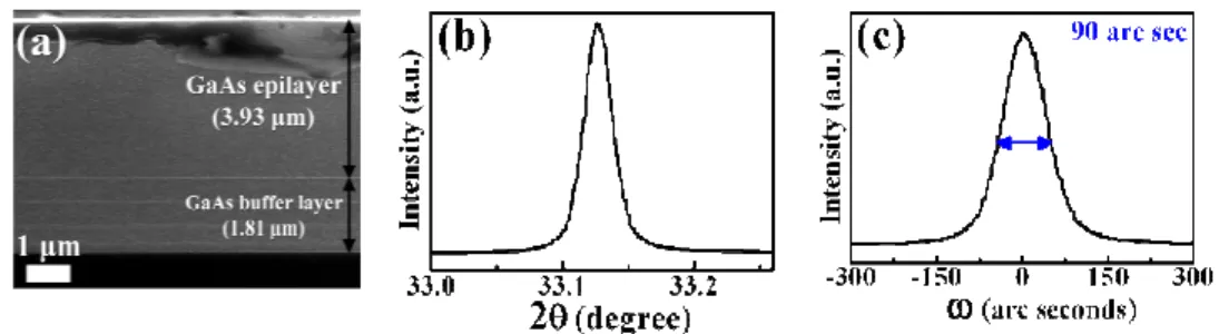
Fig. 1(a) shows the cross-sectional SEM micrograph of the GaAs epilayer grown on Si substrates. The thickness of the GaAs epilayer and the GaAs buffer layer were found to be 3.93 and 1.81 µm, respectively. The structural properties of the GaAs epilayers were analyzed after the epitaxial growth. Fig. 1(b) shows the typical XRD 2θ-ω scan of the GaAs epilayers. A sharp reflection at 33.13° for the GaAs (002) plane was observed.18 The rocking curve of the (002) diffraction pattern from GaAs epilayers is displayed in Fig. 1(c). The full width at half maximum (FWHM) of the rocking curve for the (002) plane is 90 arcsec, indicating a very good quality of GaAs epilayers on Si substrates.19
Fig. 1. (a) The cross-sectional SEM view of GaAs epilayers on Si substrates (b) The XRD pattern of the GaAs epilayer. (c) The rocking curve of (002) diffraction peak of the GaAs epilayer.
RSC
Advances
Accepted
Manuscript
4
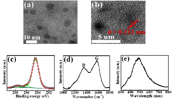
Fig. 2. (a) TEM image of graphene quantum dots (GQDs). (b) HRTEM image of an individual GQD. (c) XPS C1s analysis of GQDs. (d) Raman spectrum of GQDs. (e) PL spectrum of GQDs under the excitation wavelength of 260 nm.
Fig. 2(a) shows the TEM image of the synthesized GQDs. The diameters of the GQDs were distributed in the range of 7-12 nm, with an average of ~8 nm. The sizes of the synthesized GQDs using pulsed laser ablation are generally consistent with those synthesized by a hydrothermal approach described in the previous report.15 The high resolution TEM (HRTEM) of a GQD is shown in Fig. 2(b), displaying a crystalline structure with an interplanar spacing of 0.212 nm, which is the (102) lattice fringes of graphene.17 To investigate the chemical structure of GQDs, XPS measurements were carried out. Fig. 2(c) show the C1s XPS spectrum of GQDs. The C1s signal was deconvoluted into three peaks at 284.4, 286.3, and 287.7 eV binding energies, corresponding to the sp2 aromatic carbon (C=C), epoxy groups (C-O), and carbonyl groups (C=O), respectively.20 Similar functional groups determined by XPS has been reported for GQDs previously.20 Fig. 2(d) displays the Raman spectrum of the as-prepared GQDs synthesized by pulsed laser ablation. The well-known D band at ~1351 cm-1 and the G band at ~1589 cm-1 were clearly observed, which represent the defect-induced breathing mode of aromatic rings and the optical E2g phonons at the Brillouin
zone center, respectively.17 The intensity ratio of the D and G bands is a measure of disorder degree and is inversely proportional to the average size of the sp2 crystallite domain. The average crystallite size La can be determined according to.21-22
, (1)
where I(D) is the integrated intensity of the D band, I(G) is the integrated intensity of the G band, and C(λ) is an empirical constant which depends on the wavelength of the excitation
a L C G I D I( ) ( )= (λ)
RSC
Advances
Accepted
Manuscript
5
laser. According to Eq. (1), the average crystallite size La was estimated to be 5.2 nm,
comparable with the previous result in GQDs.18 The PL of GQDs is displayed in Fig. 2 (e), revealing a broad PL band that peaks at around 485 nm. The PL spectrum is in good agreement with those of GQDs in previous reports.14,21 The PL in GQDs has been demonstrated to be associated with the localized electron-hole pairs, oxygen-containing functional groups, intrinsic/extrinsic states.23-27 The PL emission peak of the synthesized GQDs shifts toward the long-wavelength region as the excitation wavelength increases (not shown). Similar broad PL spectra and excitation-dependent PL behaviors have been reported for GQDs synthesized from top-down approaches.12 Although the GQDs can be prepared by other methods such as hydrothermal as well as acid treatment and chemical exfoliation routes,14-15 those methods are sometimes limited by the critical synthesis conditions (high temperatures) and time consuming.The synthesis using pulse laser ablation in the aqueous graphene is a one-step, fast, and reliable method for preparation of GQDs.
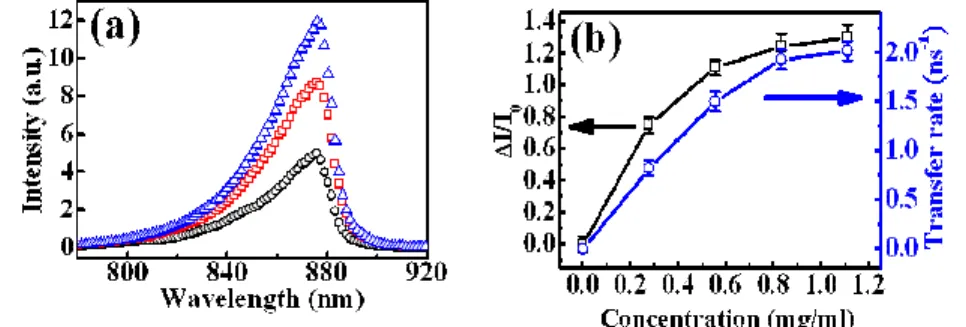
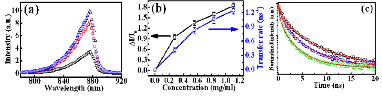
Fig. 3. (a) PL spectra of the GaAs epilayers after incorporation of GQDs with different concentration: 0 (open circles), 0.28 mg/ml (open squares), and 0.84 mg/ml (open triangles). (b) The PL intensity ratio of the GaAs with GQDs to that of the untreated GaAs as a function of the GQD concentration. The carrier transfer rate as a function of the GQD concentration is also shown. The lines are guides for eyes.
The open circles in Fig. 3(a) show the PL spectrum of the GaAs epilayer without introduction of GQDs. The PL peak wavelength is about 878 nm, assigned as the band-to-band transition in GaAs. The asymmetric shape of PL spectrum is associated with the low defect density in epilayers.28 The FWHM of the GaAs epilayer was determined to be 26 meV, indicating a high quality of GaAs epilayers on Si substrates also.28 The open squares and triangles in Fig. 3 (a) show PL spectra of GaAs layers after incorporation of GQDs with the concentration of 0.28 and 0.84 mg/ml, respectively. The PL intensity from GaAs increases as the concentration of GQDs increases. The PL intensities as a function of the GQD concentration are shown as the open squares in Fig. 3(b). The PL intensity has a maximum value at the GQD concentration of 0.84 mg/ml, revealing an enhancement of PL intensity by a factor of 2.3.
RSC
Advances
Accepted
Manuscript
6
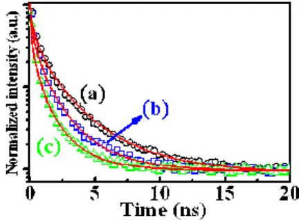
Fig. 4. The PL decay profiles of the GQDs deposited on GaAs epilayers with the GQD concentration of (a) 0(circles), (b) 0.28 (squares), and (c) 0.84 (triangles) mg/ml. The time-resolved PL was performed under the excitation wavelength of 260 nm. The solid lines show the fitted curves using Eq. (2).
To find out the origin of PL enhancement, time-resolved PL measurements were performed. The open circles in Fig. 4(a) displays the PL decay profile of bare GQDs (on a glass) monitored at the wavelength of 460 nm. The PL decay curve was fitted by the stretched exponential function:
, (2) where represents carrier densities and k represents the decay rate of carriers and is a dispersive exponent. The solid line in Fig. 4(a) shows the fitted result, in good agreement with experiments. In the stretched exponential function the average decay time is calculated as follows:29
, (3) where Γ is the Gamma function. It is known that a decrease in the PL decay time is associated with a decrease in the carrier density. If the decrease of PL decay time in GQDs is in parallel to the enhancement of PL in GaAs epilayers, we can deduce that the enhanced PL intensity in GaAs comes from the carriers in GQDs. In the absence of GaAs, the PL decay rate of bare GQDs can be represented by . Owing to the presence of an extra decay channel in GQDs, the PL decay rate of GQDs in the hybrid case (i.e. GQDs on GaAs) can then be described by:
, (4) where is rate of the carrier transfer from GQDs to GaAs. The carrier transfer rate can thus be determined from Eq. (4) and is listed in Table 1. The open circles and triangles in Fig. 4 show the PL decay curves of GQDs on top of the GaAs with the concentration of 0.28 and 0.84 mg/ml, respectively. The PL decay transients in the GQDs on GaAs decay more pronouncedly as compared with that in bare GQDs, indicating the presence of carrier transfer from GQDs to GaAs. The PL decay curves in Figs. 4 (b) and (c) were also fitted by the
β t) (
)
0
(
)
(
t
n
e
kn
=
− ) 1 ( 1 β β τ >= Γ < k ) (t n 1 − GQDτ
β 1 1 1 − − −+
=
GQD CT hybridτ
τ
τ
1 − CTτ
RSC
Advances
Accepted
Manuscript
7
stretched exponential function and the carrier transfer rates were determined using Eqs. (2)-(4). All the fitting parameters and the obtained average decay times are listed in Table 1. The open circles in Fig. 3(b) show the carrier transfer rate as a function of the GQD concentration. It was found the carrier transfer rate increases with increasing the amount of GQD concentration. The carrier transfer rate has a maximum value at the concentration of 0.84 mg/ml, and then saturates after that concentration.
Table 1 The dispersion components , the decay rates k, the PL decay times of GQDs, and the rates of the carrier transfer versus the GQD concentration.
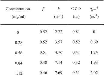
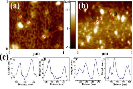
It is well known that the PL intensity depends on the penetration depth of the incident light, which is a measure of the sample thickness that is detected. If the thickness of the GQD layer is thicker than the penetration depth of the incident light, the effective GQD concentration would somewhat decreases, leading to an ambiguity of the PL intensity (enhancement). Therefore, it is necessary to figure out the penetration depth of the incident light and the thickness of the GQDs. The penetration depth, which is the inverse of the absorption coefficient, is not available in literature. However, it could be found out approximately from the absorption coefficient of reduced graphene oxide and was found to be ~500 nm for the excitation wavelength of 660 nm.30 On changing excitation wavelength from 532 to 260 nm, the penetration length of laser was estimated from ~500 to ~100 nm. To determine the GQD thickness, AFM measurements were performed. Figs. 5(a) and 5(b) show AFM images of GQDs with the concentration of 0.28 and 1.12 mg/ml, respectively. The average heights of GQDs were mostly found to be ~11 and ~12 nm for the concentration of 0.56 and 1.12 mg/ml, respectively (Fig. 5(c)). This indicates that the average height only increases little for increasing the GQD concentration. Rather, the GQD density increases pronouncedly as the GQD concentration increases. The above results reveal that the GQD thickness (~11-12 nm) is much thinner than the light penetration length (~100-500 nm). All
Concentration (mg/ml) β k (ns-1) > <
τ
(ns) τCT-1 (ns-1) 0 0.28 0.56 0.84 1.12 0.52 0.52 0.51 0.48 0.46 2.22 3.57 4.76 7.14 7.69 0.81 0.52 0.41 0.32 0.31 0 0.69 1.24 1.93 2.02 βRSC
Advances
Accepted
Manuscript
8
the carriers in GQDs can thus be generated by photoexcitation and transfer to the GaAs epilayer for PL. The ambiguity of PL intensity due to the partial absorption of GQDs can thus be excluded.
Fig. 5. AFM images of GQDs with the concentration of (a) 0.28 mg/ml and (b)1.12 mg/ml. (c) The height profile along the lines extracted from (a) and (b).
The open circles in Fig. 6(a) show the PL of the GaAs epilayer without and with GQDs under the excitation wavelength of 400 nm. Similar to the result in Fig. 3(a), the PL intensity from GaAs epilayers increases as the GQD concentration increases. The PL intensities as a function of the GQD concentration are shown as the open squares in Fig. 6(b). The maximum PL intensity has an enhancement factor as high as 2.8, which is larger than that (2.3) with the excitation wavelength of 532 nm. We suggest that an excitation with the shorter wavelength (higher energy) may generate carriers with higher kinetic energy, injecting to a deeper region in the GaAs epilayer and leading to a larger PL enhancement. Fig. 6(c) shows the PL decay profiles of GQDs without and with GQDs under the excitation wavelength at 400 nm. The open circles in Fig. 6(b) show the carrier transfer rate as a function of the GQD concentration. Similar to the result in Fig. 3(b), the carrier transfer rate increases with the GQD concentration for the excitation wavelength at 400 nm. However, the carrier transfer rate for the excitation at 400 nm is smaller than that for the excitation at 260 nm. This result may be explained by the generation of the lower-energy carriers for the 400-nm excitation light, which limits the transfer of photoexcited carriers and leads to a lower carrier transfer rate.
RSC
Advances
Accepted
Manuscript
9
Fig. 6. The PL decay profiles of the GQDs deposited on GaAs epilayers with the GQD concentration of (a) 0(circles), (b) 0.28 (squares), and (c) 0.84 (triangles) mg/ml. The time-resolved PL was performed under the excitation wavelength of 400 nm. The solid lines show the fitted curves using Eq. (2).
To explore the mechanism of carrier transfer from GQDs to GaAs, Kelvin probe measurements for work function of GQDs and GaAs were carried out. The contact potential difference (VCPD) between the sample and tip can be related to the difference
in work function between them from the following equation:
, (5) where Wtip and Wsample are work functions of the tip and sample, respectively, and e is the
elementary charge. By measuring VCPD , the sample work function can be estimated as long as
the work function of the tip (Wtip) is determined. Before measuring the GQD and GaAs
samples, Wtip was calibrated through a separate measurement by taking VCPD on the Au film
(with known work function value of 5.1 eV). The subsequent VCPD measurements determined
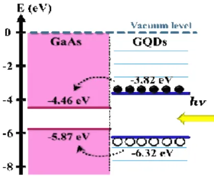
the work function of GQDs and GaAs to be 4.46 ± 0.02 eV and 3.82 ± 0.03 eV, respectively. The values of their work functions are comparable with the reported values in literature.9,15 On the basis of Kelvin probe measurements, the carrier transfer process from GQDs to GaAs under illumination can be interpreted by a band diagram of GQDs and GaAs, as shown in Fig. 7. When GQDs are incorporated on top of GaAs epilayers, the carriers generated by optical excitation are able to transfer from GQDs to GaAs through the GQD/GaAs interface because the work function of GQDs (3.82 eV) is smaller than that of GaAs (4.46 eV). The carrier transfer leads to an additional radiative recombination of carriers in the GaAs region and produces an enhancement of PL intensity in GaAs. Due to the removal of photogenerated carriers in GQDs, recombination of the electron-hole pairs in GQDs would be reduced and the PL transient for GQDs decreases accordingly. At higher concentrations of GQDs, more carriers in GQDs can be generated by photoexcitation, leading to an increase of the carrier transfer rate and a pronounced PL enhancement in GaAs. Thus, the carriers in GQDs are effectively transfer to GaAs, leading to a higher enhancement of PL in GaAs, as displayed in Figs. 3(b) and 6(b). sample tip CPD W W eV = −
RSC
Advances
Accepted
Manuscript
10
Fig. 7 Energy band diagram of GaAs in contact with GQDs, describing the carrier transfer.
Although this study has been focused on the GaAs material, the proposed method should also be extended to other semiconductors of which work function is larger than that of GQDs. Also, this result indicates that introducing the GQDs on the semiconductor surface can be a convenient way for enhancing the PL intensity in semiconductors, which will promise great potential in optoelectronic devices or bio-imaging.
4. CONCLUSIONS
In summary, a one-step method for the synthesis of GQDs by pulse laser ablation from the aqueous graphene has been demonstrated. The synthesized GQDs with an average size of 8 nm were obtained by analysis of the TEM image. The effect of GQDs on the enhancement of PL in GaAs epilayers has also been demonstrated. As the concentration of GQDs increases, the PL intensity in GaAs increases accordingly. The PL intensity of GaAs has a maximum enhancement with a factor of 2.8 at the GQD concentration of 0.84 mg/ml. We suggest that the carrier transfer owing to the work function difference between GQDs and GaAs is responsible for the enhancement of the PL intensity in GaAs.
Acknowledgments. This project was supported in part by the Institute of Nuclear Energy Research under the grant number 1042001INER010 and the Ministry of Science and Technology in Taiwan under the grant number MOST 103-2112-M-003-004-MY3.
RSC
Advances
Accepted
Manuscript
11
References:
1. K. S. Novoselov, A. K. Geim, S. V. Morozov, D. Jiang, Y. Zhang, S. V. Dubonos, I. V. Grigorieva, and A. A. Firsov, Science, 2004, 306, 666-669.
2. C. Berger, Z. Song, X. Li , X. Wu, N. Brown, C. Naud, D. Mayou, T. Li, J. Hass, A. N. Marchenkov, E. H. Conrad, P. N. First, and W. A. de Heer, Science, 2006, 312, 1191-1196. 3. K. S. Kim, Y. Zhao, H. Jang, S. Y. Lee, J. M. Kim, K. S. Kim, J. H. Ahn, P. Kim, J. Y. Choi, and
B. H. Hong, Nature, 2009, 457, 706-710.
4. S. Stankovich, D. A. Dikin, G. H. B. Dommett, K. M. Kohlhaas, E. J. Zimney, E. A. Stach, R. D. Piner, S. T. Nguyen, and R. S. Ruoff., Nature, 2006, 442, 282-286.
5. A. K. Geim and K. S. Novoselov, Nature Mater., 2007, 6, 183-191.
6. G. Eda, G. Fanchini, and M. Chhowalla, Nat. Nanotechnol., 2008, 3, 270-274.
7. H. Ajlani, R. Othmen, M. Oueslati, A. Cavanna, and A. Madouri, J. Vac Sci. Technol. B, 2013, 31, 020602.
8. L. Wang, Y. Zhang, X. Li, E. Guo, Z. Liu, X. Yi, H. Zhu, and G. Wang, RSC Adv., 2013, 3, 3359-3364.
9. S. Tongay, M. Lemaitre, X. Miao, B. Gila, B. R. Appleton, and A. F. Hebard, Phys. Rev. X, 2012, 2, 011002.
10. J. Chen, J. Shi, X. Wang, H. Cui, and M. Fu, Chin. J. Catal., 2013, 34, 621-640.
11. J. Hou, C. Yang, H. Cheng, Z. Wang, S. Jiao, and H. Zhu, Phys. Chem. Chem. Phys., 2013, 15, 15660-15668.
12. M. A. Sk., A. Ananthanarayanan, L. Huang, K. H. Lim, P. Chen, J. Mater. Chem. C, 2014, 2, 6954-6960.
13. K. J. Williams, C. A. Nelson, X. Yan, L. Li, and X. Zhu, ACS Nano, 2013, 7, 1388-1394. 14. W. Chen, F. Li, C. Wu, and T. Guo, Appl. Phys. Lett., 2014, 104 063109.
15. J. Zhao, L. Tang, J. Xiang, R. Ji, Y. Hu, J. Yuan, J. Zhao, Y. Tai, and Y. Cai, RSC Adv., 2015, 5, 29222-29229.
16. P. Yu, X. Wen, Y. Toh, Y. Lee, K. Huang, S. Huang, S. Shrestha, G. Conibeer, and J. Tang, J. Mater.
Chem. C, 2014, 2, 2894-2901.
17. T. N. Lin, K. H. Chih, C. T. Yuan, C. C. Yang, J. L. Shen, C. A. J. Lin, and W. R. Liu, Nanoscale,
RSC
Advances
Accepted
Manuscript
12 2015, 7, 2708-2715.
18. S. V. Novikov, K. W. Edmonds, A. D. Giddings, K. Y. Wang, C. R. Staddon, R. P. Campion, B. L. Gallagher, and C T Foxon, Semicond. Sci. Technol., 2004, 19, L16-L16.
19. Y. Alaskar , S. Arafin, D. Wickramaratne, M. A. Zurbuchen, L. He, J. McKay, Q. Lin, M. S. Goorsky, R. K. Lake, and K. L. Wang, Adv. Funct. Mater., 2014, 24, 6624-6638.
20. X. Zhou, Y. Zhang, C. Wang, X. C. Wu, Y. Q. Yang, B. Zheng, H. Wu, S. Guo, and J. Zhang, ACS
Nano, 2012, 6, 6592-6599.
21. S. H. Song, M. Jang, J. Chung, S. H. Jin, B. H. Kim, S. Hur, S. Yoo, Y. Cho, and S. Jeon, Adv.
Optical Mater., 2014, 2, 1016-1023.
22. T. Gokus, R. R. Nair, A. Bonetti, M. Böhmler, A. Lombardo, K. S. Novoselov, A. K. Geim, A. C. Ferrari, and A. Hartschuh, ACS Nano, 2009, 3, 3963-3968.
23. K. P. Loh, Q. Bao, G. Eda, and M. Chhowalla, Nat. Chem., 2010, 2, 1015-1024.
24. S. Zhu, J. Zhang, S. Tang, C. Qiao, L. Wang, H. Wang, X. Liu, B. Li, Y. Li, W. Yu, X. Wang, H. Sun, and B. Yang, Adv. Fun. Mater., 2012, 22, 4732-4740.
25. F. Liu, M. H. Jang, H. D. Ha, J. H. Kim, Y. H. Cho, and T. S. Seo, Adv. Mater., 2013, 25, 3657-3662.
26. L. Wang, S. J. Zhu, H.Y. Wang, S. N. Qu, Y. L. Zhang, J. H. Zhang, Q. D. Chen, H. L. Xu, W. Han, B. Yang, and H. B. Sun, ACS Nano, 2014, 8, 2541-2547.
27. X. Wen, P. Yu, Y. Toh, X. Hao, and J. Tang, Adv. Opt. Mater., 2013, 1, 173-178. 28. C. W. Hsu, Y. F. Chen, and Y. K. Su, Nanotechnol., 2012, 23, 495306.
29. A. F. van Driel, I. S. Nikolaev, P. Vergeer, D. Vanmaekelbergh, and W. L. Vos, Phys. Rev. B, 2007,
75, 035329.
30. R. Su, S. F. Lin, D. Q. Chen, and G. H. Chen, J. Phys. Chem. C, 2014, 118, 12520-12525.
RSC
Advances
Accepted
Manuscript
13
Graphical contents entry
The effect of graphene quantum dots (GQDs) on the enhancement of PL in GaAs epilayers has been demonstrated and interpreted by the carrier transfer due to the work function difference.