Growth of high-quality epitaxial ZnO
films on (10–10) sapphire by atomic layer
deposition with
flow-rate interruption method
Jheng-Ming Huang
a, Ching-Shun Ku
b, Hsin-Yi Lee
b,c,⁎
, Chih-Ming Lin
d, San-Yuan Chen
ca
Program for Science and Technology of Accelerator Light Source, National Chiao Tung University, Hsinchu 300, Taiwan
bNational Synchrotron Radiation Research Center, 101 Hsin-Ann Road, Hsinchu Science Park, Hsinchu 30076, Taiwan c
Department of Materials Science and Engineering, National Chiao Tung University, Hsinchu 300, Taiwan
d
Department of Applied Science, National Hsinchu University of Education, Hsinchu 30076, Taiwan
a b s t r a c t
a r t i c l e i n f o
Available online 25 May 2012 Keywords:
Atomic-layer deposition Flow-rate interruption ZnO
X-ray diffraction
A novel process in an atomic layer deposition system with“flow-rate interruption” (FRI) was developed to obtain epitaxial ZnOfilms of high quality. The m-plane ZnO thin films were grown on m-plane sapphire sub-strates by atomic layer deposition with FRI or a conventional continuous-flow method at the temperature in the range of 25–260 °C; 200 °C appeared optimal. Measurements of X-ray reflectivity indicated that the thick-ness of ZnOfilms with FRI is almost twice than that grown with the continuous-flow method. The structural, optical and electrical properties were investigated with X-ray diffraction (XRD), photoluminescence and Hall measurements. The diffraction results indicated that the interruptedflow might extend the reaction of dieth-ylzinc and water through an increased duration to improve the crystallographic quality of the films. According to the results from XRD at high resolution, to substantiate the epitaxial relation between the thinfilm and the substrate, an off-normal azimuthal scan along ZnO (201) demonstrated two-fold symmetry that indicated the ZnOfilms to be in epitaxial growth on sapphire. The photoluminescence results showed a strongly enhanced near-band-edge emission of an FRI sample, and the donor–bond exciton appearing in films also indicated superior crystalline qualities. The Hall mobility of the FRI method was up to 64.7 cm2V− 1s− 1. The FRI method evidently improved the structural, optical and electrical properties of the ZnOfilms with small consumption of precursors.
© 2012 Elsevier B.V. All rights reserved.
1. Introduction
ZnO is an attractive material for many applications because of its direct band gap and large binding energy (60 meV) of its excitons [1], larger than for GaN (26 meV)[2]and thermal energy(~25 meV) near 300 K; these properties make ZnO a promising candidate for near-UV optoelectronic devices near 300 K. For the development of material science and the realization of optoelectronic applications,
ZnOfilms are grown with various techniques, such as sol–gel method
[3], radio-frequency magnetron sputtering[4], pulsed laser
deposi-tion (PLD)[5], metal-organic chemical-vapor deposition (MOCVD)
[6], molecular-beam epitaxy (MBE) [7] or atomic-layer deposition
(ALD)[8]. Some authors observed, however, that ZnO could generate
a spontaneous polarization along the c-axis direction and internal
electricfields in the multi-quantum well (MQW) structures[9]. The
internal electricfield separates the electrons and holes present after
excitation, decreasing the overlap of their respective wave functions and their radiative transitions. The phenomenon was called
quantum-confined Stark effect (QCSE)[10]which would have
nega-tive effects on the optical and electrical properties of devices. To di-minish the polarization effects, several authors proposed to grow
ZnOfilms along semi-polar or non-polar directions, such as in the
a-plane, m-plane and r-plane[10–12]. In this work, we deposited
ZnOfilms on m-plane sapphire.
Among several deposition techniques, ALD is promising for
growth offilms because of its several advantages, such as low
tem-perature, accurate and simple control of thickness, capability and uni-formity of a large area, satisfactory reproducibility. According to conventional ALD, the precursors are introduced into the growth chamber sequentially, followed by sustained pumping to evacuate
the superfluous reactants. This method is generally called
‘continu-ous-flow (CF)’ or ‘flow-type’ ALD[13]. To obtain epitaxial ZnOfilms
of high quality at low temperature, we developed a novel ALD process
withflow-rate interruption (FRI)[14]. In the present work, we
inves-tigated the influence of growth with the FRI and CF methods on the
crystalline structure, and the optical electrical properties of a ZnO
thinfilm grown on m-plane sapphire substrates with ALD. To
charac-terize the structure and thickness of the ZnOfilms, high-resolution
X-ray diffraction (HRXRD) and X-ray reflectivity (XRR) were
per-formed. The photoluminescence (PL) was used to investigate the
⁎ Corresponding author at: National Synchrotron Radiation Research Center, 101 Hsin-Ann Road, Hsinchu Science Park, Hsinchu 30076, Taiwan. Tel.: + 886 3 5780281.
E-mail addresses:[email protected](C-S. Ku),[email protected](H-Y. Lee). 0257-8972/$– see front matter © 2012 Elsevier B.V. All rights reserved. doi:10.1016/j.surfcoat.2012.05.067
Contents lists available atScienceDirect
Surface & Coatings Technology
j o u r n a l h o m e p a g e : w w w . e l s e v i e r . c o m / l o c a t e / s u r f c o a toptical properties whereas the electrical properties were measured with the Hall effect.
2. Experiments
The ZnOfilms were deposited on m-plane (10–10) sapphire
sub-strates with ALD via a novel FRI technique and a conventional CF method. Diethylzinc (DEZn) and DI water were applied as precursors of Zn and O, respectively. The growth conditions of both FRI and CF
methods are listed inTable 1. To determine the variation of the thin
film deposition rates under different growth temperature and the re-lationship between the crystalline quality and orientation, the HRXRD and XRR techniques were applied.
The X-ray scattering measurements were performed at the wig-gler X-ray beamline BL-17B1 in the National Synchrotron Radiation Research Center (NSRRC), Hsinchu, Taiwan. Two pairs of slits be-tween the sample and the detector enabled a typical wave-vector
res-olution of ~0.001 nm− 1 in the vertical scattering plane in this
experiment.
The PL was measured at 12 K on samples using a He-Cd laser (325 nm, IK3252R-E, Kimmon) for excitation and with a CCD (cooled with liquid nitrogen to 80 K, Spec-10, Princeton Instruments) and a monochromator (0.5 m, SP-2558A, Acton) for detection. The effective resolution in the PL spectrum was 0.02 nm. The Hall effect was mea-sured (NI PXI-1024Q AC system, National Instruments) with a
mag-neticfield 0.68 T.
3. Result and discussion
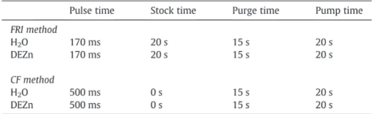
Wefirst defined the optimal deposition temperature to be 200 °C
assessed from the XRD intensity. As can be seen from the inset of Fig. 1, the integrated intensity of the ZnO (200) reflection for both FRI and CF series have maximal intensity at 200 C. Second, to
determine the crystalline quality, optical and electrical properties at the same standard thickness, we performed measurements on ZnO films of the same thickness, 240 nm, grown at 200 °C with FRI and CF, determined by measurement of X-ray diffraction, PL and the Hall
effect, for thickness 240 nm of ZnOfilms with FRI during ~1200 ALD
cycles and with CF during ~ 1800 ALD cycles.
The crystallinity of the ZnO thinfilms grown by ALD on the
m-plane sapphire with varied substrate temperature were investigated using HRXRD. The values of H, K, and L in this paper are appropriate to an orthorhombic crystal system and are expressed in reciprocal lat-tice units (r. l. u.) referring to parameters of the sapphire latlat-tice a = 0. 8245, b = 0.475, c = 1.2993 nm and the ZnO lattice, a = 0.5628,
b = 0.325, c = 0.5207 nm at 25 °C. The reflection signal was measured
from a radial scan (θ−2θ scan) along the surface normal of m-plane
ZnO thinfilms with a (200) orientation relative to hexagonal ZnO
(10–10) at 2θ=31.737 .Fig. 1show the surface normal radial scan
HRXRD spectra for ZnO thinfilms with growth temperature in the
range of 25–260 °C by ALD of FRI method and CF method. ZnO thin
films in both series were deposited with 100 ALD cycles. The results show that the ZnO (200) signal became a dominant phase for a
depo-sition temperature above 100 °C. The diffraction intensity reflects the
crystalline quality and increased with increasing growth temperature up to 200 °C for the FRI method. In addition, the XRD patterns of the FRI method also show distinct tight fringes that became increasingly symmetric both near either side of the (200) signal and extending farther than with the CF method for a growth temperature near
200 °C. This evidence indicates that the ZnOfilms grown with the
FRI method were thicker andflatter than with the CF method. In the
inset ofFig. 1, the integrated intensity of the ZnO (200) reflection
for both FRI and CF series, indicating that the FRI series had a greatly increased intensity for a growth temperature in the range of
120–260 °C and for both series the optimal temperature is 200 °C.
Fig. 2shows experimental results of XRR (open circles) and their
bestfitted results (solid line). The simulation of the specular
reflectiv-ity is based on the recursive formalism of Parratt[15]to acquire the
physical parameters of the ZnO thinfilms. With the Mercury code
[16]we determined the physical parameters of thefilms, including
roughness and thickness. The growth rates and roughness of the
ZnOfilms calculated from the fitted results of XRR are shown in the
inset ofFig. 2, which clearly indicate a greater rate of growth for the
FRI method over all the growth range because the stock mode
pro-vides a sufficient duration for the precursors to react with the
sub-strate surface in the growth chamber. The growth window with a flat growth curve of the FRI method in the range of 60–220 °C
Table 1
Growth conditions of ZnOfilms on m-plane sapphire deposited at 25 to 260 °C. Pulse time Stock time Purge time Pump time FRI method H2O 170 ms 20 s 15 s 20 s DEZn 170 ms 20 s 15 s 20 s CF method H2O 500 ms 0 s 15 s 20 s DEZn 500 ms 0 s 15 s 20 s 40 80 120 160 200 240 280 0 50 100 150 200 28 30 32 34 36 38 40 10-4 100 104 108 1012 1016 1020 2 (degree)
FRI
Intensity (arb. units)
(200) 25oC 40oC 60oC 80oC 180oC 220oC 240oC 260oC 100oC 120oC 140oC 200oC 25oC 40oC 60oC 80oC 180oC 220oC 240oC 260oC 100oC 120oC 140oC 200oC 28 30 32 34 36 38 40 2 (degree)
CF
(200)Intensity (arb. units)
Growth temperature (oC) FRI
CF
seems wider than for the CF method in the range of 80–200 °C. Below 100 °C the growth rate decreased because the thermal energy was
in-sufficient to overcome the potential barrier of the chemical reaction.
In contrast, above 200 °C the growth rate decreased at higher temper-ature because the greater thermal energy induced surface decomposi-tion or desorpdecomposi-tion. Several authors reported that the growth rate decreased in the temperature range above the growth window with
increasing substrate temperature [8,17–19]. The XRR fitting also
yields the surface roughness shown in the inset ofFig. 2. The surface
roughness obtained from XRRfitting is consistent with AFM measure
result (not shown here). The results indicate that ZnOfilms grown
with FRI have smoother surfaces than with CF within the specified
range of temperature, in agreement with the distribution of fringes
in the FRI ZnO (200) signal shown inFig. 1.
The FRI method yielded a superior surface roughness for a thick film and satisfactory crystalline quality at 200 °C. To compare the
two growth methods in a fair manner, we grew ZnOfilms of the
same thickness and measured the crystalline quality, optical and
elec-trical properties. We compared the ZnOfilms of the same thickness,
240 nm, grown at 200 °C with FRI with 1200 ALD cycles and CF meth-od with 1800 ALD cycles.
Fig. 3shows a radial scan along the (H 0 0)-direction at the surface
normal of ZnOfilms. The values of H depended on parameters of the
sapphire lattice a = 8.245. There appear three reflection signals,
re-spectively ZnO (200), ZnO (400) and sapphire (600) inFig. 3, the
in-tensity of the ZnO (200) grown with the FRI method (solid squares)
was 3 times that with the CF method (open circles). To examine the behavior of the epitaxial relation between ZnO and sapphire, we
in-troduced an off-normal azimuthal scan as shown inFig. 4which
ex-hibits the off-normal azimuthal scan curve of ZnO (110) and (201). The full width at half maximum (FWHM) of the FRI method was 1.272° (broad band) and 0.0211° (narrow band) respectively, which are narrower than 1.513° (broad band) and 0.0246° (narrow band)
of the CF method. Thefilm/substrate interface alignment of the FRI
method was better than with the CF method;Fig. 4clearly exhibits
a two-fold symmetry between ZnO (201) and sapphire (310). No other feature was observed in the intervals between the two lines, indicating a perfect alignment of c and b-axes of ZnO unit cells
along those of the sapphire substrate. These results providefirm
ev-idence that a strongly epitaxial layer was deposited on the substrate by both methods. The reciprocal space mapping (RSM) results in Fig. 5and the azimuthal scan ofFig. 4indicate that an epitaxial
rela-tion between ZnO and sapphire follows [201]ZnO‖[310]sapphire and
[310]ZnO‖[404]sapphire. Moreover, the broad line of ZnO (201) was
also broader than that of ZnO (110). In previous work[20], we
obtained the in-plane relation between ZnO and m-sapphire follows
[020]ZnO‖[006]sapphire and [002]ZnO‖[020]sapphire, and identified a
2 3 4 5 6 10-4 10-2 100 102 104 106 2.9 3.0 10 100 1000 FRI CF Sapphire (600) ZnO (400) H=5.848 ZnO (200) H=2.924
Intesity (arb. units)
H (r. l. u.)
H (r. l. u.)
Intesity (arb. units)
Fig. 3. Radial scan along the surface normal of ZnOfilms with the FRI and CF methods with the same thickness, 240 nm.
-90 0 90 180 270 106 1011 1016 1021 1026 1031 Sapphire (310) FRI CF CF FRI ZnO (110) ZnO (110)
Intensity (arb. units)
ZnO (201) ZnO (201)
Phi (degree)
Fig. 4. Azimuthal scans (Φ scan) of the ZnO film peak and the substrate Bragg peak with both methods, including ZnO (110), ZnO (201) and sapphire (310).
0 40 80 120 160 200 240 280 0 4 0 40 80 120 160 200 240 280 0.08 0.16 0.24 0.32 0 1 2 3 4 5 6 Data
Intensity (arb. units)
2 (degree) 2 (degree) FRI CF 25oC 40oC 60oC 80oC 180oC 220oC 240oC 260oC 100oC 120oC 140oC 200oC 25oC 40oC 60oC 80oC 180oC 220oC 240oC 260oC 100oC 120oC 140oC 200oC 10-4 102 108 1014 1020 1026 1032 Fitted line 0 1 2 3 4 5 6 FRI CF Roughness (nm)
Substrate temperature (oC) FRI
CF
Growth rate(nm/cycle)
Substrate Temperature (oC)
Fig. 2. X-ray reflectivity and their best fitted curves of ZnO films (100 cycles) with growth temperature in the range of 25–260 °C. The inset shows the growth rate and roughness obtained from thefitted results for both of the FRI and CF methods.
large lattice mismatch (~ 9.38%) between sapphire (020) and ZnO (002). It is thus reasonable that the FWHM of ZnO (110) was
narrower than for ZnO (201). InFig. 5, mosaicity results in the
elon-gation of the layer signal along the in-plane direction (K and L) and were not completely aligned along the normal direction (H),
indicat-ing almost full relaxation of strain in ZnOfilms of thickness 240 nm,
but the gradient curves of ZnO with the FRI method focused more on ZnO (201) and ZnO (310) points in reciprocal space signify a small
lattice distribution and indicate greater crystalline quality.Figs. 4
and 5show not only that the ZnOfilms were confirmed to be
epitax-ialfilms but also that the FRI method improved the crystalline quality
of these ZnOfilms.
The results of PL measurements are shown inFig. 6. Thefilms
de-posited with the FRI method (solid squares) exhibit strong
near-band-edge (NBE) emission (D0X) at 3.364 eV[21]. Thefilms deposited
with the FRI method show more intense NBE emission than from the CF method, and also determined that the optical properties of the
ZnOfilms were greatly improved with the FRI method, in agreement
with the comparison of crystalline quality. The emission signal near
3.0 eV for ZnOfilms from the CF method might be contributed by
stac-king faults[22]to promote the production of accepter states in ZnO
films, preferring to recombine between donor and acceptor[23].
Table 2shows the electrical resistivity, mobility and carrier
con-centration of ZnOfilms with the FRI and CF methods measured with
2.0 2.4 2.8 3.2 3.6 102 103 104 : FRI : CF Intesity (arb. units)
Photon energy (eV)
D
0X 3.364
Fig. 6. PL measurements of ZnOfilms: FRI and CF methods.
Table 2
Mobility, resistivity and carrier concentration obtained from Hall measurements. Mobility (cm^2/Vs) R (/ohm-cm) Carrier concentration (N/cm^3) FRI method 64.7 (± 0.2) 1.0 × 10− 2(± 0.1) −9.5×10¹⁸(± 0.2) CF method 34.8 (± 0.3) 2.5 × 10− 3(± 0.2) −6.8×10¹⁹ (± 0.3) 3.9 4.0 4.1 4.2 4.0 4.1 4.2 4.3 4.4 4.5 Sapphire (404) L (r. l. u) H (r. l. u.) 3.9 4.0 4.1 4.2 L (r. l. u) Sapphire (404) ZnO (310) 0.8 0.9 1.0 1.1 2.7 2.8 2.9 3.0 ZnO (201) Sapphire (310) K (r. l. u) K (r. l. u) H (r. l. u.) 0.8 0.9 1.0 1.1 ZnO (201) Sapphire (310)
FRI
CF
CF
FRI
ZnO (310)the Hall effect. The growth offilms with FRI clearly presents a great-er mobility, greatgreat-er resistivity and smallgreat-er carrigreat-er concentration
than from the CF method. The ZnO films as-grown typically
exhibited n-type conductivity and a native carrier, attributed to
in-trinsic defects, such as zinc interstitials and oxygen vacancies[24].
The green–yellow luminescence of ZnO was due to oxygen vacancies
in the ZnO crystals[25]. Apart from the intrinsic defects, the absence
of green–yellow luminescence in PL spectra and greater electrical
resistivity were in agreement with the superior crystalline quality with the FRI method.
4. Conclusion
We investigated the effect of growth temperatures in the range of
25–260 °C on the structure of m-plane ZnO on m-plane sapphire with
FRI and CF methods. Both methods had an optimum temperature at
200 °C. The roughness and growth rate of ZnOfilms improved with
FRI in the range of 60–220 °C of the growth window. The duration
of the precursor pulses with the FRI method compared with the CF method indicated that the FRI method can decrease the consumption
of precursors. The epitaxial relation of ZnOfilms of thickness 240 nm
on m-plane sapphire is confirmed. The FRI method showed a strongly
improved crystalline quality, optical properties and electrical mobility
of ZnOfilms.
Acknowledgment
This work was partially supported by the National Science Council of Taiwan, under grant no. NSC-99-2221-E-213-002-MY2.
References
[1] A. Mang, K. Reimann, S. Rubenacke, Solid State Commun. 94 (1995) 251. [2] M.A. Reshchinov, H. Morkoç, J. Appl. Phys. 97 (2005) 061301. [3] S. O'Brien, L.H.K. Koh, G.M. Crean, Thin Solid Films 516 (2008) 1391. [4] J. Lu, Y. Zhang, Z. Ye, L. Wang, B. Zhao, J. Huang, Mater. Lett. 57 (2003) 3311. [5] Z.K. Tang, G.K.L. Wong, P. Yu, M. Kawasaki, A. Ohtomo, H. Koinuma, Y. Segawa,
Appl. Phys. Lett. 72 (1998) 3270.
[6] B.P. Zhang, K. Wakatsuki, N.T. Binh, N. Usami, Y. Segawa, Thin Solid Films 449 (2004) 12.
[7] F.X. Xiu, Z. Yang, L.J. Mandalapu, D.T. Zhao, J.L. Liu, W.P. Beyermann, Appl. Phys. Lett. 87 (2005) 152101.
[8] J. Lim, C. Lee, Thin Solid Films 515 (2007) 3335.
[9] P. Waltereit, O. Brandt, A. Trampert, H.T. Grahn, J. Menniger, M. Ramsteiner, M. Reiche, K.H. Ploog, Nature 406 (2000) 865.
[10] M.M.C. Chou, L. Chang, D.R. Hang, C. Chen, D.S. Chang, C.A. Li, Cryst. Growth Des. 9 (2009) 2073.
[11] R. Deng, B. Yao, Y.F. Li, B.H. Li, Z.Z. Zhang, H.F. Zhao, J.Y. Zhang, D.X. Zhao, D.Z. Shen, X.W. Fan, L.L. Yang, Q.X. Zhao, J. Cryst. Growth 311 (2009) 4398. [12] J.M. Chauveau, D.A. Buell, M. Laugt, P. Vennegues, M. Teisseire-Doninelli, S.
Berard-Bergery, C. Deparis, B. Lo, B. Vinter, C. Morhain, J. Cryst. Growth 301–302 (2007) 366.
[13] S.Y. Pung, K.L. Choy, X. Houand, C. Shan, Nanotechnology 19 (2008) 435609. [14] C.S. Ku, H.Y. Lee, J.M. Huang, C.M. Lin, Thin Solid Films 518 (2009) 1373. [15] L.G. Parratt, Phys. Rev. 95 (1954) 359.
[16] D.K. Bowen, B.K. Tanner, Nanotechnology 4 (1993) 175. [17] A. Yamada, B. Sang, M. Konagai, Appl. Surf. Sci. 112 (1997) 216. [18] E.B. Yousfi, J. Fouache, D. Lincot, Appl. Surf. Sci. 153 (2000) 223.
[19] E.B. Yousfi, B. Weinberger, F. Donsanti, P. Cowache, D. Lincot, Thin Solid Films 387 (2001) 29.
[20] C.S. Ku, H.Y. Lee, J.M. Huang, C.M. Lin, Cryst. Growth Des. 10 (2010) 1460. [21] H.J. Ko, Y.F. Chen, Z. Zhu, T. Yao, Appl. Phys. Lett. 76 (2000) 1905.
[22] M. Schirra, R. Schneider, A. Reiser, G.M. Prinz, M. Feneberg, J. Biskupek, U. Kaiser, C.E. Krill, K. Thonke, R. Sauer, Phys. Rev. B 77 (2008) 125215.
[23] J. Sun, H. Liang, J. Zhao, Q. Feng, J. Bian, Z. Zhao, H. Zhang, Y. Luo, L. Hu, G. Du, Appl. Surf. Sci. 254 (2008) 7482.
[24] D.C. Look, J.W. Hemsky, J.R. Sizelove, Phys. Rev. Lett. 82 (1999) 2552.
[25] K. Vanheusden, C.H. Seager, W.L. Warren, D.R. Tallant, J.A. Voigt , Appl. Phys. Lett. 68 (1996) 403.