Effects of Process and Gate Doping Species on
Negative-Bias-Temperature Instability of p-Channel MOSFETs
Da-Yuan Lee,aTiao-Yuan Huang,aHorng-Chih Lin,b,zWan-Ju Chiang,a Guo-Wei Huang,band Tahui WangaaInstitute of Electronics, National Chiao-Tung University, Hsinchu 300, Taiwan bNational Nano Device Laboratories, Hsinchu 300, Taiwan
The effects of poly-Si gate doping type and species as well as thermal treatments on negative-bias-temperature instability共NBTI兲 of p-channel metal-oxide-semiconductor field effect transistors 共MOSFETs兲 were investigated. We found that devices with n⫹-poly-Si gate depict a smaller threshold voltage shift after bias-temperature stressing, compared to their p⫹-poly-Si-gated counterparts. By carefully controlling the thermal budget to suppress boron penetration, NBTI can be reduced by fluorine incorporation in p⫹-poly-Si-gated devices. Finally, NBTI is found to be aggravated in devices subjected to H2 postmetal-annealing, highlighting the important role of hydrogen bonds.
© 2004 The Electrochemical Society. 关DOI: 10.1149/1.1639168兴 All rights reserved.
Manuscript submitted April 23, 2003; revised manuscript received August 29, 2003. Available electronically January 9, 2004.
For aggressively scaled deep submicrometer complementary ox-ide semiconductor共CMOS兲 ultra large scale integrated 共ULSI兲 tech-nologies, an ultrathin gate oxide is essential for achieving high cur-rent drive under low power operation. The integrity and reliability of such gate oxides are therefore crucial for ULSI manufacturing. Re-cently, negative-bias-temperature instability共NBTI兲 has been iden-tified as a major reliability concern for deep sub-micrometer p-channel metal-oxide-semiconductor 共MOS兲 transistors.1-4 Large numbers of interface states and positive fixed charges are generated during bias-temperature stressing 共BTS兲, and cause an unwanted negative threshold shift in device characteristics, which could poten-tially lead to circuit failure. This phenomenon becomes even more pronounced as the oxide is thinned down, and may become the limiting factor for the device lifetime. It has also been shown that NBTI could be further aggravated by process-induced damages such as plasma charging,4-6 and boron penetration.2,4 Special attention should therefore be paid to exploring and understanding the influ-ence of different processing steps and treatments on device charac-teristics.
In this paper, we characterized the NBTI of devices with differ-ent process treatmdiffer-ents. Dependences of gate-doping types, gate, and source/drain共S/D兲 doping species, and postmetal annealing treat-ments were investigated. Some interesting findings were obtained, which could help clarify the role of different species incorporated in the device.
Experimental
Complementary MOS 共CMOS兲 transistors used in this study were fabricated on 6 in. silicon wafers with a resistivity of 10-25⍀ cm. After local oxidation of silicon共LOCOS兲 isolation and threshold voltage (Vth) adjustment implantation, the gate oxide was ther-mally grown in a diluted O2 ambient at 900°C. Oxide thickness measured by a n&k analyzer共and also confirmed by capacitance-voltage, C-V measurements that took into account the poly-depletion effect兲 on the monitor wafers before poly-Si deposition was around 3.0 nm. Undoped poly-Si layer was then deposited by low-pressure chemical vapor deposition共LPCVD兲. For p-MOS de-vices with n⫹-poly-Si gate, As⫹ ions (5⫻ 1015cm⫺2) were im-planted immediately after poly-Si gate deposition. While for the p⫹-gated p-MOS devices, gate and source/drain共S/D兲 implants were performed simultaneously by either BF2⫹or B⫹共both with a dose of 2.5⫻ 1015cm⫺2) implantation. The post-S/D implant thermal treat-ments were carefully controlled to ensure that boron penetration was effectively suppressed in our samples.
Details of the structural parameters and process conditions for devices characterized in this study are summarized in Table I. In this work, we focus our attention on the NBTI characteristics of devices with different gate-doping types and species as well as post-metal annealing treatments. To evaluate degradations due to the bias-temperature stress, devices were subjected to stress conditions with negative gate bias共⫺3.5-⫺4.5 V兲 at 150°C. During stressing, drain/ source and substrate were all grounded, as shown in Fig. 1. To evaluate the role of hydrogen atoms in the NBTI, the post-metal anneal共PMA兲 performed in a forming gas was intentionally skipped for some samples. Device parameters, including threshold voltage, subthreshold swing 共SS兲, transconductance, and gate leakage cur-rent, were measured using an HP4156A parameter analyzer both before and after the BT stressing.
Results and Discussion
Effects of poly-Si gate doping type.—Threshold voltage shift as a
function of bias temperature共BT兲 stressing time for samples 1 and 2 is shown in Fig. 2. It can be seen that Vth degradation obeys the power law7,8
⌬Vth共t兲 ⫽ Atb 关1兴
The extracted A and b values for the measured data as well as the initial gate current under the stress conditions, are summarized in Table II. The extracted b values are around 0.25-0.30 for all devices. These results are consistent with previous reports,7implying that the incorporated As⫹ ion in the poly-Si gate would not effectively change the mechanisms of NBTI. Note that the initial stress current for sample 1 (n⫹-gated兲 is about an order of magnitude higher than that of sample 2 (p⫹-gated兲. From Fig. 2, it can be seen that the n⫹-gated device shows a much smaller Vth shift under BTS than its p⫹-gated counterpart, albeit with a similar b value. Figure 3 com-pares the pre-BTS gate leakage current for fresh samples 1 and 2. For a given gate voltage (Vg), sample 1共i.e., n⫹-gated兲 exhibits a higher leakage current. This could be explained by the band dia-grams shown in Fig. 4. For sample 1, the leakage current is domi-nated by the electron Fowler-Nordheim 共F-N兲 tunneling from the n⫹-gate共Fig. 4b兲, which has a much higher probability than either the gate valence-band electron direct-tunneling or the substrate hole-tunneling process for sample 2共Fig. 4a兲.9Though the higher elec-tron injection flux from the n⫹-gate would result in almost the same time dependence共Table I兲, the Vth shift is much smaller than that of the p⫹-gated device, indicating that the electron tunneling current plays only a minor role in the NBTI degradation. Also note in Fig. 4, the oxide field is stronger for the p⫹-gated device. This also supports the argument that the oxide field plays a key role in NBTI degradation.10
Figure 1. Configuration for NBTI stressing.
Figure 2. Threshold voltage shift as a function of BT stressing time for
devices with different gate doping types共solid line for n⫹-gated sample 1 and dashed line for p⫹-gated sample 2兲.
Figure 3. Gate leakage current vs. gate bias for samples 1 and 2.
Figure 4. Band diagrams of 共a兲 p⫹-gated 共sample 2兲 and 共b兲 n⫹-gated 共sample 1兲 p-MOSFETs with n-substrate, biased at Vg ⫽ ⫺4 V.
Table I. Major structural parameters and process conditions for the test samples.
Sample no. 1 2 3 4 5
Lgate 0.8m
Wgate 10m
Tox 2.9-3.1 nm
Gate doping type n⫹ p⫹ p⫹ p⫹ p⫹
Deep S/D implant (2.5⫻ 1015cm⫺2) BF2 ⫹ BF 2⫹ B⫹ B⫹ BF2⫹ S/D extension (5⫻ 1014cm⫺2) BF2 ⫹ BF 2⫹ BF2⫹ B⫹ BF2⫹
PMA Yes Yes Yes Yes No
Table II. Fitting parameters for Eq. 1 and the initial stress gate leakage for all samples.
Sample splits and BTS condition Vth of fresh devices共V兲 A Exponent b Ja 共A/cm2 兲 Sample 1,⫺4 V 1.629 1.32 0.28 369nm Sample 1,⫺4.5 V 1.622 3.05 0.30 3.31m Sample 2,⫺4 V 0.615 5.56 0.27 46.8 nm Sample 2,⫺4.5 V 0.616 9.89 0.28 876nm Sample 3,⫺4 V 0.636 12.32 0.24 40.3 nm Sample 4,⫺4 V 0.623 11.84 0.25 42.6 nm Sample 5,⫺4 V 0.639 4.87 0.26 43.2 nm
Effects of fluorine incorporation.—In this study, fluorine was
in-corporated during the deep and/or S/D extension implant steps 共Table I兲. Various amounts of fluorine incorporation could thus be obtained, and the resultant effects on the device performance were explored. Figure 5 shows the cumulative probability of the threshold voltages (Vth) for the fabricated devices. The tight Vth distribution in Fig. 5 indicates that there is no noticeable boron penetration effect induced in these devices. Figure 6 shows the prestress C-V curves. Equivalent oxide thickness共EOT兲 of the samples is extracted using a simulator that takes quantum mechanical and poly-depletion ef-fects into consideration. An EOT of around 2.9 nm is obtained for the devices without or with only a small amount 共i.e., through a medium dose BF2extension implant兲 of fluorine incorporation. EOT
Figure 5. Cumulative probability of the threshold voltages (Vth) for sample
2共with highest fluorine incorporation, 䊏兲, sample 3 共with intermediate fluo-rine incorporation,䊐兲, and sample 4 共without any deliberate fluorine incor-poration,䊉兲.
Figure 6. High frequency C-V characteristics for sample 2共with highest
fluorine incorporation,䊏兲, sample 3 共with intermediate fluorine incorpora-tion,䊐兲, and sample 4 共without any deliberate fluorine incorporation, 䊉兲.
Figure 7. Vth shift as a function of stress time, stressed at 150°C, Vg
⫽ ⫺4 V.
Figure 8. 共a兲 Fresh and 共b兲 post-BTS charge-pumping currents for sample 2
共with highest fluorine incorporation, 䊏兲, sample 3 共with intermediate fluorine incorporation,䊐兲, and sample 4 共without any deliberate fluorine incorpora-tion,䊉兲.
Table III. Extracted pre- and post-BTS interface state density
„Dit… for samples with different SÕD implant conditions.
Sample splits Dit共pre-BTS兲 ⌬Dit 共post-BTS兲
Sample 2 4.03⫻ 1010共1/eV cm2兲 9.34⫻ 1010共1/eV cm2兲 Sample 3 8.35⫻ 1010共1/eV cm2兲 1.56⫻ 1011共1/eV cm2兲 Sample 4 9.16⫻ 1010共1/eV cm2兲 1.76⫻ 1011共1/eV cm2兲
increases to 3.1 nm when a high-dose BF2⫹implant is performed. The apparent oxide thickness increase with high fluorine incorpora-tion is consistent with previous reports.10,11
In Fig. 7, the Vth shift as a function of stress time is shown for devices with different S/D implant conditions共i.e., samples 2, 3, and 4, respectively, see Table I兲. As can be seen in this figure, the NBTI could be reduced effectively by increasing fluorine incorporation, although the slope is almost identical among all splits. To gain in-sight into the effect of fluorine incorporation at the Si/SiO2 inter-face, a charge-pumping technique was also performed for detail analysis. Figure 8a shows the results for fresh devices. All transis-tors are with a width-length of 5m/0.8 m. The results indicate that the addition of fluorine reduces the interface states. Figure 8b shows charge-pumping current increments after BT stressing. The interface state density extracted from the results shown in Fig. 8a and 8b is summarized in Table III. Again, charge-pumping current decreases with increasing fluorine incorporation, and the sample with the highest fluorine incorporation共i.e., sample 2 that received fluorine incorporation both from BF2⫹S/D extension and deep S/D BF2⫹ implants兲 indeed shows the best performance. The ratios of the increased Dit among the splits are close to those of the Vth shift. This result indicates that the incorporated F atoms, which could replace hydrogen-related sites at the Si/SiO2interface, tend to pas-sivate the interface dangling bonds. Since the SiuF bonding energy 共5.73 eV兲 is higher than that of SiuH bond 共3.18 eV兲,12 proper fluorine incorporation at the Si/SiO2interface could improve NBTI immunity.
It should be noted that fluorine incorporation has been previously reported to cause enhanced boron penetration, which in turn could enhance the NBTI.2,7 Since the thermal budget is carefully con-trolled to prevent the occurrence of boron penetration, proper fluo-rine incorporation actually strengthens the interface10,13 and thus improves the NBTI immunity in our study.
Effects of PMA.—PMA in a forming gas was widely used for
passivation of the interface dangling bonds. However, the passivated SiuH bonds tend to break more easily during subsequent NBTI
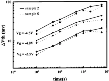
stressing. The released hydrogen atoms could diffuse into the oxide bulk, and cause a threshold voltage shift.1To understand the effects of passivated SiuH bonds at SiO2/Si interface during BT stress, NBTI immunity of devices both with共i.e., sample 2兲 and without 共i.e., sample 5兲 PMA treatments were measured and compared. Fig-ure 9 shows the subthreshold characteristics of the test samples. The pre- and poststress subthreshold swings for both devices are sum-marized in Table IV. Although the device without PMA shows poorer initial subthreshold characteristics, it depicts a smaller sub-threshold swing degradation共about 1.66%兲 during BTS, compared to the device with PMA treatment共2.75%兲. This is ascribed to more SiuH bond breaking during BTS for the PMA-treated device. Fig-ure 10 shows the Vth shift as a function of BTS stress time. Indeed the device with PMA shows more severe NBTI degradation. These results unambiguously highlight the important role of hydrogen in the NBTI degradation process.
Conclusions
The effects of gate doping species and thermal treatments on negative-bias-temperature instability共NBTI兲 of p-MOSFETs were conducted. Devices with n⫹-poly-Si gate exhibit less NBTI degra-dation, compared to their p⫹-gated counterparts. Our analysis indi-cates that the electron FN tunneling current during stressing plays only a minor role in the NBTI degradation. By contrast, the oxide field strength is critical for the NBTI degradation process. Our re-sults also indicate that fluorine incorporation by a S/D implant step is beneficial for improving the NBTI immunity. The incorporated fluorine could replace hydrogen-related sites at the SiO2/Si inter-face, which could act as precursors for the generation of interface traps responsible for NBTI degradation.
The effects of PMA on device characteristics were also investi-gated. We found that, although the incorporated hydrogen atoms could reduce the pre-BTS interface states, the passivated hydrogen could be released during BTS, causing aggravated NBTI degrada-tion.
Acknowledgments
The authors thank the staff at National Nano Device Laboratories for their assistance in device fabrication. This work was supported in part by the National Science Council of the Republic of China under contract no. NSC90-2215-E009-079.
National Nano Device Laboratories assisted in meeting the publication costs of this article.
Figure 9. Pre- and post-BTS subthreshold characteristics for sample 2共with
PMA兲 and sample 5 共without PMA兲. Figure 10. Vth shift vs. BT stress time for sample 25共without PMA兲. 共with PMA兲 and sample
Table IV. Pre- and post-BTS SS for samples with and without post-metal anneal.
Sample splits Sample 2共with PMA兲 Sample 5共wt % PMA兲
Before BTS 81.21 mV/dec 91.14 mV/dec
References
1. T. Yamamoto, K. Uwasawa, and T. Mogami, IEEE Trans. Electron Devices, 46, 921共1999兲.
2. N. Kimizuka, T. Yamamoto, T. Mogami, K. Yamaguchi, K. Imai, and T. Horiuchi, in Proceedings of Symposium on VLSI Technology, 73共1999兲.
3. N. Kimizuka, K. Yamaguchi, K. Imai, T. Iizuka, C. T. Liu, R. C. Keller, and T. Horiuchi, in Proceedings of Symposium on VLSI Technology, 92共2000兲. 4. A. T. Krishnan, V. Reddy, and S. Krishnan, Tech. Dig. - Int. Electron Devices
Meet., 2001, 865.
5. D. Y. Lee, H. C. Lin, M. F. Wang, M. Y. Tsai, T. Y. Huang, and T. Wang, in Proceedings of Solid State Devices and Materials, 204共2001兲.
6. F. E. Pagaduan, J. K. J. Lee, V. Vedagarbha, K. Lui, M. J. Hart, D. Gitlin, T. Takaso, S. Kamiyama, and K. Nakayama, in Proceedings of the 39th IEEE Annual
Inter-national Reliability Physics Symposium, 315共2001兲.
7. C. H. Liu, M. T. Lee, C. Y. Lin, J. Chen, K. Schruefer, J. Brighten, N. Rovedo, T. B. Hook, M. V. Khare, S. F. Huang, C. Wann, T. C. Chen, and T. H. Ning, Tech. Dig. - Int. Electron Devices Meet., 2001, 861.
8. K. O. Jeppson and C. M. Svensson, J. Appl. Phys., 48, 2004共1977兲.
9. Y. Shi, T. P. Ma, S. Prasad, and S. Dhanda, IEEE Trans. Electron Devices, 45, 2355 共1998兲.
10. T. B. Hook, E. Adler, F. Guarin, J. Lukaitis, N. Rovedo, and K. Schruefer, IEEE Trans. Electron Devices, 48, 1346共2001兲.
11. P. Wright and K. C. Saraswat, IEEE Trans. Electron Devices, 36, 879共1989兲. 12. C. C. Chen, H. C. Lin, C. Y. Chang, C. C. Huang, C. H. Chien, T. Y. Huang, and M.
S. Liang, in Proceedings of Symposium on Plasma Process Induced Damage, 121 共2000兲.