This content has been downloaded from IOPscience. Please scroll down to see the full text.
Download details:
IP Address: 140.113.38.11
This content was downloaded on 25/12/2014 at 03:22
Please note that terms and conditions apply.
Effects of layer sequence and postdeposition annealing temperature on performance of
La2O3 and HfO2 multilayer composite oxides on In0.53Ga0.47As for MOS capacitor
application
View the table of contents for this issue, or go to the journal homepage for more 2014 Appl. Phys. Express 7 031201
(http://iopscience.iop.org/1882-0786/7/3/031201)
Effects of layer sequence and postdeposition annealing temperature on performance
of La
2O
3and HfO
2multilayer composite oxides on In
0.53Ga
0.47As for MOS capacitor application
Wen-Hao Wu1, Yueh-Chin Lin1, Ting-Wei Chuang1, Yu-Chen Chen1, Tzu-Ching Hou1, Jing-Neng Yao1,
Po-Chun Chang1, Hiroshi Iwai2, Kuniyuki Kakushima2, and Edward Yi Chang1,3
1Institute of Materials Science and Engineering, National Chiao-Tung University, Hsinchu 30010, Taiwan, R.O.C. 2Tokyo Institute of Technology, Meguro, Tokyo 152-8550, Japan
3Department of Electronics Engineering, National Chiao-Tung University, Hsinchu 30010, Taiwan, R.O.C. E-mail: [email protected]
Received November 20, 2013; accepted January 29, 2014; published online February 13, 2014
In this paper, we report on high-k composite oxides that are formed by depositing multiple layers of HfO2and La2O3on In0.53Ga0.47As for MOS device application. Both multilayer HfO2(0.8 nm)/La2O3(0.8 nm)/In0.53Ga0.47As and La2O3(0.8 nm)/HfO2(0.8 nm)/In0.53Ga0.47As MOS structures were investigated. The effects of oxide thickness and postdeposition annealing (PDA) temperature on the interface properties of the composite oxide MOS capacitors were studied. It was found that a low CET of 1.41 nm at 1 kHz was achieved using three-layer composite oxides. On the other hand, a small frequency dispersion of 2.8% and an excellent Dit of 7.0' 1011cm%2&eV%1 can be achieved using multiple layers of La2O3(0.8 nm) and HfO2(0.8 nm) on the In0.53Ga0.47As MOS capacitor with optimum thermal treatment and layer thickness.
©2014 The Japan Society of Applied Physics
R
ecently, InxGa1¹xAs metal–oxide–semiconductor field-effect transistors (MOSFETs) have been widely investigated owing to the high electron mobility of the InxGa1¹xAs material and the much lower turn-on voltage of InxGa1¹xAs devices than of conventional Si devices.1–4)Rare-earth oxides (REOs) exhibit high dielectric constant and high conduction band offset with respect to silicon and are currently being investigated as high-k gate dielectrics for future ultrascaled devices.5–9) Among the binary REOs, La2O3 is considered as one of the most promising gate
dielectric materials owing to its high ¬ and high band-gap energy. However, strong interdiffusion between InGaAs and La2O3 occurs after postdeposition annealing (PDA) when
La2O3is in direct contact with the InxGa1¹xAs material.10)In
recent years, several groups have studied composite oxides such as HfO2/Al2O3,11) CeO2/Al2O3,12) and CeO2/HfO213)
on InGaAs for next-generation device applications.
In this work, high-k composite oxides of La2O3and HfO2
are investigated for n-In0.53Ga0.47As MOS capacitor
applica-tion. HfO2 is chosen because it has ak of 25 and an energy
band gap of 5.5 eV, and is known to demonstrate inversion behavior with InxGa1¹xAs.14–18) An in situ molecular beam
deposition (MBD) system was used to deposit the multiple layers of HfO2(0.8 nm) and La2O3 (0.8 nm) on n-In0.53
-Ga0.47As. The effects of PDA temperature and annealing gas
atmosphere on the interface properties and device perform-ances of HfO2/La2O3/n-In0.53Ga0.47As and La2O3/HfO2/
n-In0.53Ga0.47As MOS capacitors are studied.
The device structure includes a 100 nm In0.53Ga0.47As layer
with 5© 1017cm¹3 Si doping grown on the n-InP substrate by molecular beam epitaxy (MBE). The device process can be divided into four parts: surface treatment, oxide deposi-tion, gate metal deposideposi-tion, and ohmic contact formation. The wafers were first cleaned in 4% HCl solution for 3 min, followed by an (NH4)2S solution dip for 30 min at room
temperature. Then, the wafers were loaded into the MBD system to deposit the HfO2(0.8 nm)/La2O3(0.8 nm)
multi-layers on n-In0.53Ga0.47As at 300 °C. The 10 layers of HfO2
(0.8 nm) and La2O3(0.8 nm) MOS capacitors were fabricated
and annealed at temperatures ranging from 400 to 550 °C in N2for 5 min. Then, Ni/Au was deposited on the front side of
the wafer as the gate contact metal and Au/Ge/Ni/Au was
deposited on the back side of the n+ InP substrate as ohmic metal; both were deposited using an e-beam evaporator and the ohmic metal was annealed at 250 °C for 30 s for optimum contact resistance.
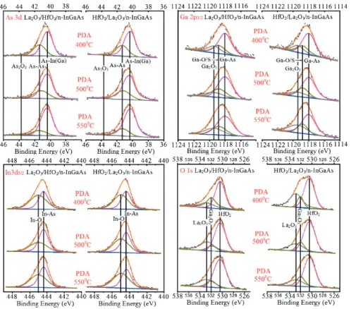
Figure 1 shows the X-ray photoelectron spectros-copy (XPS) spectra of the HfO2(0.8 nm)/La2O3(0.8 nm)/
n-In0.53Ga0.47As and La2O3 (0.8 nm)/HfO2(0.8 nm)/n-In0.53
-Ga0.47As composite oxide structures annealed at 400, 500,
and 550 °C in N2for 5 min. The As 3d, Ga 2p3/2, In 3d5/2,
and O 1s XPS spectra of the samples with different PDA temperatures were analyzed to determine the film composi-tions and interface properties. In general, with increasing PDA temperature, more interactions between oxides and semiconductors occur, and the number of As–As bonds is reduced owing to the high-temperature annealing, as indi-cated by As 3d in Fig. 1. When the PDA temperature was increased to 500 °C, the amounts of As-, Ga-, and In-related oxides decreased for both composite oxide structures. The amount of La2O3 increased for the La2O3/HfO2/n-In0.53
-Ga0.47As structure, as indicated by the XPS O 1s peak in
Fig. 1. The slight reduction of the native oxides could be explained by the conversion of As–O, Ga–O, and In–O bonds to InAs, GaAs, and La2O3 during thermal annealing for
the La2O3/HfO2/n-In0.53Ga0.47As structure. However, the
amount of La2O3 that diffused into InGaAs increased with
temperature for the HfO2/La2O3/n-In0.53Ga0.47As structure.
The 500 °C annealing not only converted the As–O, Ga–O, and In–O bonds to InAs and GaAs bonds but also resulted in the increase in the amount of La2O3diffusing into InGaAs
for the HfO2/La2O3/n-In0.53Ga0.47As structure. Furthermore,
the amounts of As-, Ga-, and In-related oxides increased significantly for both composite oxide structures when the PDA temperature was increased to 550 °C, as indicated by the As 3d, Ga 2p3/2, and In 3d5/2 spectra in Fig. 1. This indicates that at the PDA temperature of 550 °C, the diffusions of As, Ga, and In into the oxide layers were quite significant for both composite oxide structures.
Figure 2 shows the comparison of capacitance–voltage (C–V) curves at 1 MHz for the five layers of HfO2(0.8 nm)/
La2O3(0.8 nm) and the five layers of La2O3(0.8 nm)/
HfO2(0.8 nm) composite oxides on n-In0.53Ga0.47As MOS
capacitors, and the HfO2 (8 nm)/n-In0.53Ga0.47As MOS http://dx.doi.org/10.7567/APEX.7.031201
capacitor. The electrical characteristics of the composite oxide MOS capacitor were markedly improved when the devices were annealed at the PDA temperature of 500 °C in N2 for 5 min. The dielectric constants of 15.2 and 14.8
were estimated for the five layers of the La2O3(0.8 nm)/
HfO2(0.8 nm) and HfO2 (0.8 nm)/La2O3(0.8 nm) composite
oxides on n-In0.53Ga0.47As MOS capacitors, respectively.
Some reports show that the semiconductor elements will diffuse into the oxide after annealing, resulting in the decrease in the oxide dielectric constant and the increase in the device capacitance equivalent thickness (CET).19)In this case,
CET ¼ "0"SiO2
Cðaccum:@ f ¼ 1 kÞ;
where C(accum.@ f = 1 kHz) is the capacitance of the accumulation region at frequency= 1 kHz, ¾0is the vacuum
permittivity, and ¾SiO2 is relative permittivity of SiO2. A
CET of 2.2 nm at 1 kHz with a low interface trap den-sity (Dit) of 7.0© 1011cm¹20eV¹1was achieved, as estimated
by the conductance method20) for the La
2O3/HfO2/
n-In0.53Ga0.47As capacitor, as shown in Fig. 3(a). A higher
Ditand a lower CET were obtained for the HfO2(0.8 nm)/
La2O3(0.8 nm)/n-In0.53Ga0.47As device owing to the strong
interaction between La2O3 and n-In0.53Ga0.47As. When the
PDA temperature was increased, the interaction between the oxide and the semiconductor increased. The Gp/wqA vs frequency plot and Dit vs energy plot for the 5 layers
of La2O3(0.8 nm)/HfO2 (0.8 nm) and HfO2(0.8 nm)/
La2O3(0.8 nm) on n-In0.53Ga0.47As MOS capacitors with
PDA at 500 °C are shown in Figs. 4(a) and 4(b), respec-tively. From Fig. 4(b), the lowDitof 7.0© 1011–1.0 © 1012
cm¹20eV¹1 in the energy range of 0.47–0.44 eV above the In0.53Ga0.47As valence band maximum was obtained for
the La2O3 (0.8 nm)/HfO2 (0.8 nm)/n-In0.53Ga0.47As device.
When the PDA temperature was increased to 550 °C, the capacitance decreased from 1.46 (500 °C) to 1.39 µF/cm2
(550 °C) and 1.44 (500 °C) to 1.20 µF/cm2 (550 °C) for
the La2O3/HfO2/n-In0.53Ga0.47As structure and HfO2/La2O3/
n-In0.53Ga0.47As structure, respectively. The larger
capaci-tance decrease, particularly for the HfO2(0.8 nm)/La2O3
(0.8 nm)/n-In0.53Ga0.47As capacitor, was due to the strong
interdiffusion between La2O3and InGaAs after
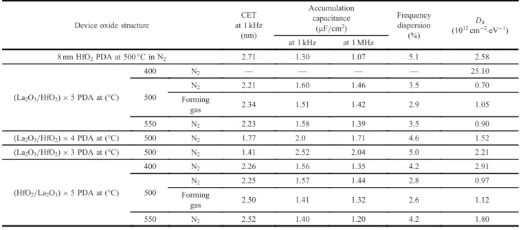
high-temper-ature annealing. The C–V characteristics of the composite oxide capacitors with PDA temperatures of 400, 500, and 550 °C and different oxide thicknesses are compared in Table I.
Fig. 1. As 3d, Ga 2p3/2, In 3d5/2, and O 1s XPS spectra of La2O3(0.8 nm)/HfO2(0.8 nm)/n-In0.53Ga0.47As and HfO2(0.8 nm)/La2O3(0.8 nm)/
n-In0.53Ga0.47As with postdeposition annealing temperatures of 400, 500, and 550 °C in nitrogen gas for 5 min.
Fig. 2. Comparison ofC–V characteristics of HfO2(8 nm)/
n-In0.53Ga0.47As, La2O3(0.8 nm)/HfO2(0.8 nm)/n-In0.53Ga0.47As and
HfO2(0.8 nm)/La2O3(0.8 nm)/n-In0.53Ga0.47As MOS capacitors.
Appl. Phys. Express 7, 031201 (2014) W.-H. Wu et al.
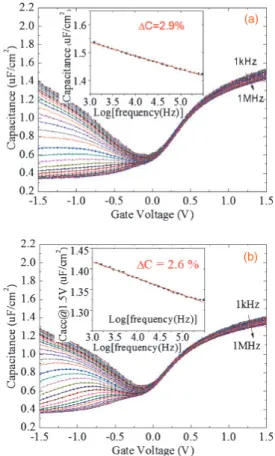
Furthermore, the device performance was further improved by forming gas (5% H2+ 95% N2) annealing. Figure 5
shows theC–V characteristics of the 5 layers of La2O3(0.8
nm)/HfO2 (0.8 nm) and the 5 layers of La2O3(0.8 nm)/
HfO2(0.8 nm) on n-In0.53Ga0.47As MOS capacitors with
PDA at 500 °C in forming gas for 5 min. Frequency dis-persion was improved owing to H2 treatment,21) especially
for the La2O3/HfO2/n-In0.53Ga0.47As structure. The
fre-quency dispersions were reduced from 3.5 to 2.9% and 2.8
to 2.6% for the La2O3/HfO2/n-In0.53Ga0.47As structure and
HfO2/La2O3/n-In0.53Ga0.47As structure, respectively.
How-ever, the capacitances of both devices decreased after forming (a)
(b)
Fig. 3. C–V characteristics of 5 layers of (a) La2O3(0.8 nm)/
HfO2(0.8 nm) and (b) HfO2(0.8 nm)/La2O3(0.8 nm) on n-In0.53Ga0.47As
MOS capacitors with PDA at 500 °C in N2gas for 5 min.
Table I. Comparison ofC–V characteristics of HfO2(8 nm)/n-In0.53Ga0.47As, La2O3(0.8 nm)/HfO2(0.8 nm)/n-In0.53Ga0.47As and HfO2(0.8 nm)/
La2O3(0.8 nm)/n-In0.53Ga0.47As MOS capacitors.
Device oxide structure
CET at 1 kHz (nm) Accumulation capacitance (µF/cm2) Frequency dispersion (%) Dit (1012cm¹20eV¹1) at 1 kHz at 1 MHz 8 nm HfO2PDA at 500 °C in N2 2.71 1.30 1.07 5.1 2.58
(La2O3/HfO2)© 5 PDA at (°C)
400 N2 — — — — 25.10 500 N2 2.21 1.60 1.46 3.5 0.70 Forming gas 2.34 1.51 1.42 2.9 1.05 550 N2 2.23 1.58 1.39 3.5 0.90
(La2O3/HfO2)© 4 PDA at (°C) 500 N2 1.77 2.0 1.71 4.6 1.52
(La2O3/HfO2)© 3 PDA at (°C) 500 N2 1.41 2.52 2.04 5.0 2.21
(HfO2/La2O3)© 5 PDA at (°C)
400 N2 2.26 1.56 1.35 4.2 2.91 500 N2 2.25 1.57 1.44 2.8 0.97 Forming gas 2.50 1.41 1.32 2.6 1.12 550 N2 2.52 1.40 1.20 4.2 1.80 (a) (b)
Fig. 4. (a) Gp/wqA (A: 1.33 © 10¹4cm2) vs frequency curves at different
gate biases and (b)Ditvs energy curves after 500 °C PDA for 5 layers of
La2O3(0.8 nm)/HfO (0.8 nm) and HfO2(0.8 nm)/La2O3(0.8 nm) on
n-In0.53Ga0.47As MOS devices.
gas annealing. The device CET was improved for the 3 and 4 layers of the La2O3(0.8 nm)/HfO2(0.8 nm) structure on the
n-In0.53Ga0.47As device after PDA at 500 °C for 5 min in N2
atmosphere. TheC–V curves for the 3-layer device are shown in Fig. 6; for the composite oxide with 3 and 4 layers of the La2O3 (0.8 nm)/HfO2(0.8 nm) structure, the CETs were
reduced to 1.77 and 1.41 nm, respectively, after 500 °C annealing, as measured at 1 kHz.
In summary, high-k composite dielectrics composed of La2O3 and HfO2 layers on n-In0.53Ga0.47As for MOS
capacitor application are investigated. Overall, the La2O3/
HfO2 structure on the n-In0.53Ga0.47As MOS capacitor
demonstrates better performance than the HfO2/La2O3
structure on the n-In0.53Ga0.47As MOS capacitor after thermal
treatment owing to the interaction between the composite oxides and InGaAs materials. A low CET of 1.41 nm at 1 kHz for 3 layers, a small frequency dispersion of 2.6%, and an excellentDitof 7.0© 1011cm¹20eV¹1can be achieved using
multiple layers of La2O3(0.8 nm) and HfO2(0.8 nm) on
In0.53Ga0.47As MOS capacitors with PDA at 500 °C. Acknowledgment The authors would like to thank the Ministry of Education and the National Science Council of the Republic of China for supporting this research under contract Nos. 102-2911-I-009-302 and 101-2221-E-009-173-MY2.
1) Y. Xuan, Y. Q. Wu, H. C. Lin, T. Shen, and P. D. Ye,IEEE Electron Device Lett.28, 935 (2007).
2) N. Goel, P. Majhi, C. O. Chui, W. Tsai, D. Choi, and J. S. Harris,Appl. Phys. Lett.89, 163517 (2006).
3) Y. Xuan, Y. Q. Wu, and P. D. Ye,IEEE Electron Device Lett.29, 294 (2008).
4) Y. Xuan, H. C. Lin, P. D. Ye, and G. D. Wilk,Appl. Phys. Lett.88, 263518 (2006).
5) C.-H. Chen, I. Y.-K. Chang, J. Y.-M. Lee, and F.-C. Chiu,Appl. Phys. Lett. 92, 043507 (2008).
6) W.-H. Kim, W. J. Maeng, M.-K. Kim, J. Gatineau, and H. Kim,
J. Electrochem. Soc.158, G217 (2011).
7) W.-H. Kim, M.-K. Kim, W. J. Maeng, J. Gatineau, V. Pallem, C. Dussarrat, A. Noori, D. Thompson, S. Chu, and H. Kim,J. Electrochem. Soc.158, G169 (2011).
8) M. S. Rahman, E. K. Evangelou, I. I. Androulidakis, and A. Dimoulas,
Electrochem. Solid-State Lett.12, H165 (2009).
9) Y. Nishikawa, N. Fukushima, N. Yasuda, K. Nakayama, and S. Ikegawa,
Jpn. J. Appl. Phys.41, 2480 (2002).
10) Y.-C. Lin, C.-H. Chang, K. Kakushima, H. Iwai, T.-E. Shie, G.-N. Huang, P.-C. Lu, T.-C. Lin, and E. Y. Chang,ECS Trans.35 [3], 397 (2011).
11) R. Suzuki, N. Taoka, M. Yokoyama, S. Lee, S. H. Kim, T. Hoshii, T. Yasuda, W. Jevasuwan, T. Maeda, O. Ichikawa, N. Fukuhara, M. Hata, M. Takenaka, and S. Takagi,Appl. Phys. Lett.100, 132906 (2012).
12) L. Yan, L. B. Kong, Q. Li, and C. K. Ong,Semicond. Sci. Technol.18, L39 (2003).
13) K. Karakaya, B. Barcones, Z. M. Rittersma, J. G. M. van Berkum, M. A. Verheijen, G. Rijnders, and D. H. A. Blank,Mater. Sci. Semicond. Process. 9, 1061 (2006).
14) H.-D. Trinh, Y.-C. Lin, H.-C. Wang, C.-H. Chang, K. Kakushima, H. Iwai, T. Kawanago, Y.-G. Lin, C.-M. Chen, Y.-Y. Wong, G.-N. Huang, M. Hudait, and E. Y. Chang,Appl. Phys. Lett.97, 042903 (2010).
15) É. O’Connor, S. Monaghan, R. D. Long, A. O’Mahony, I. M. Povey, K. Cherkaoui, M. E. Pemble, G. Brammertz, M. Heyns, S. B. Newcomb, V. V. Afanas’ev, and P. K. Hurley,Appl. Phys. Lett.94, 102902 (2009).
16) Y. Xuan, Y. Q. Wu, T. Shen, T. Yang, and P. D. Ye,IEDM Tech. Dig., 2007, p. 637.
17) F. Zhu, H. Zhao, I. Ok, H. S. Kim, M. Zhang, S. Park, J. Yum, S. Koveshnikov, V. Tokranov, M. Yakimov, S. Oktyabrsky, W. Tsai, and J. C. Lee,IEEE CSIC Symp., 2008, p. 100.
18) H.-D. Trinh, Y.-C. Lin, H.-C. Wang, C.-H. Chang, K. Kakushima, H. Iwai, T. Kawanago, Y.-G. Lin, C.-M. Chen, Y.-Y. Wong, G.-N. Huang, M. Hudait, and E. Y. Chang,Appl. Phys. Express5, 021104 (2012).
19) L. Sambuco Salomone, J. Lipovetzky, S. H. Carbonetto, M. A. García Inza, E. G. Redin, F. Campabadal, and A. Faigón,J. Appl. Phys.113, 074501 (2013).
20) E. H. Nicollian and A. Goetzberger,Appl. Phys. Lett.7, 216 (1965).
21) H. D. Trinh, E. Y. Chang, P. W. Wu, Y. Y. Wong, C. T. Chang, Y. F. Hsieh, C. C. Yu, H. Q. Nguyen, Y. C. Lin, K. L. Lin, and M. K. Hudait,Appl. Phys. Lett.97, 042903 (2010). -1.5 -1.0 -0.5 0.0 0.5 1.0 1.5 0.5 1.0 1.5 2.0 2.5 3.0 Capacitance (uF/cm 2 ) Gate Voltage (V) 1kHz 1MHz
Fig. 6. C–V characteristics of three layers of La2O3(0.8 nm)/
HfO2(0.8 nm) on n-In0.53Ga0.47As MOS capacitors with PDA at 500 °C in
nitrogen gas for 5 min.
(a)
(b)
Fig. 5. C–V characteristics of the five layers of (a) La2O3(0.8 nm)/
HfO2(0.8 nm) and (b) HfO2(0.8 nm)/La2O3(0.8 nm) on n-In0.53Ga0.47As
MOS capacitors with PDA at 500 °C in forming gas for 5 min.
Appl. Phys. Express 7, 031201 (2014) W.-H. Wu et al.