A New Simulation Model for Plasma Ashing
Process-Induced Oxide Degradation in MOSFET
Kuo-Feng You,
Student Member, IEEE, Ming-Chien Chang, and Ching-Yuan Wu,
Member, IEEEAbstract— Plasma ashing process-induced oxide damage is
studied quantitatively in this paper. To simulate thin gate-oxide damage due to plasma ashing process, a new equivalent circuit model is proposed by including a differential capacitance, a parasitic resistance, an offset flatband voltage, and the effects of feedback on the interface-state and trapped oxide charge densities generated during plasma ashing process. According to this new model, computation of gate oxide charging current is performed by correlating to the latent interface-state density. The test n-MOSFET devices including different antenna-ratios are measured, and excellent agreement is obtained as compared with measured results. Moreover, the deficiency of the previous model is stated and compared. In addition, the effects of substrate doping concentration on plasma-induced oxide damage are also investigated as well as those of plasma ion density, plasma uniformity, thin gate-oxide thickness. Therefore, the relationships between interface states/oxide traps and antenna ratio are linked to provide a guideline for circuit designers and the plasma ashing process-induced damage can be predicted.
I. NOMENCLATURE
Gate current density, including gate displacement current and Fowler–Nordheim tunneling current. Fowler–Nordheim tunneling current density. Gate oxide capacitance per unit area.
Parasitic capacitance per unit area, composed of Metal I, Metal II, poly-Si, etc.
Substrate depletion capacitance per unit area. Bulk series resistance.
Flatband voltage.
Potential barrier for electron current; sheath po-tential.
Plasma potential.
Potential drop from the gate to the bulk. Potential across the gate oxide.
Potential across
Cathode (anode) electric field. Electric field in the middle region.
Area of parasitic capacitance, composed of Metal I, Metal II and poly-Si etc.; antenna area. Area of the wafer exposed in plasma ambient (gate oxide).
Bohm velocity of plasma ions
Manuscript received April 3, 1997 and July 1, 1997; revised August 18, 1997. The review of this paper was arranged by Editor M. Fukuma. This work was supported by the National Science Council, Taiwan, R.O.C., under Contract NSC-86-2215-E009-034.
The authors are with the Advanced Semiconductor Device Research Labo-ratory and Institute of Electronics, National Chiao-Tung University, Hsinchu 300, Taiwan, R.O.C.
Publisher Item Identifier S 0018-9383(98)00283-4.
Electron mean thermal velocity
Permittivity of SiO
Pre-existing trap (interface-state) density. Electron (hole) trapped density.
Interface-state density.
Distance from Si substrate to electron (hole) trap centroid.
Generation rate of trapped charge.
Capture cross section of the pre-existing traps (the generated traps).
Capture cross section of the pre-existing interface states.
Free electron (plasma ion) mass.
Effective mass of the tunneling electrons in oxide (0.5 m).
Trapping efficiency. Si- barrier height.
Substrate doping concentration. Elementary charge.
Gate(field) oxide thickness.
Boltzmann (reduced Planck) constant. Electron temperature.
II. INTRODUCTION
P
LASMA processes are very important in modern IC fab-rication for polysilicon etching, oxide and metal etching, and photoresist stripping. However, potential is built up on the exposed wafer surface by collected charges in plasma ambient, resulting in electrical stress on thin gate oxide. This problem becomes serious in multi-layer metal technologies because the charges introduced by plasma process can be built up through not only floating polysilicon but also polysilicon electrically connected to interconnection metal/polysilicon lines. More-over, the exposed wafer in plasma environment will suffer from ions bombardment, resulting in physical damage. Many evidences have shown that the plasma process-induced oxide damage occurs only in nonuniform plasma ambient [1]–[4], where plasma charges are collected by the top surface of the gate or metal/polysilicon patterns during the photoresist ashing and collected by the sidewall of gate/interconnection metal layer or by the surfaces that are not covered by photoresist during plasma etching process or plasma overetching. The collected charges will build up high potential on thin gate ox-ide, generating interface states and oxide traps, and degrading breakdown voltage of thin gate oxide [5]–[9].In this paper, an equivalent circuit model to quantitatively simulate the charging and discharging thin gate oxide is proposed. In our plasma ashing model, the differential capac-itance, the substrate resistance, the flatband voltage, and the effects of feedback on the interface-state and trapped oxide charge densities generated during plasma ashing process are considered in the equivalent circuit model and the simulated results for these damages are presented. The Fowler–Nordheim (FN) constant-current stress is used to release the latent annealed interface states and oxide traps, and the charge-pumping method is used to measure the generated interface states and oxide traps. Consequently, the interface states and oxide traps related to different antenna ratios are investigated, and the simulated gate-oxide current and measured results will be correlated.
III. SURFACE CHARGING MODEL
A. Plasma Charging Model
During plasma ashing processing, the gate electrode will be charged due to the local unbalanced ions and the electron current over the RF cycle in nonuniform plasma environment and a potential will be built up on the gate electrode. This high gate voltage will force anomalous gate-oxide current flowing through the thin gate oxide, which would deteriorate the thin gate oxide severely. In nonuniform plasma ambient, the plasma current seen by a wafer placed on the electrode can be expressed by [12], [13]
(1) (2) Multiplied by the area of the wafer exposed in plasma ambient, the plasma charging current can be rewritten as
(3) where
B. The Equivalent Circuit Model
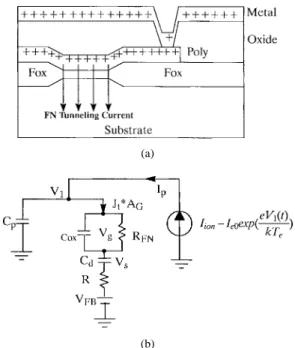
The cross section of the wafer in plasma ambient is shown in Fig. 1(a) and the equivalent circuit is shown in Fig. 1(b). Note that the testing samples are “area” type and, therefore, this model does not take the electron shading effect into account [14]. Using KCL and KVL for the circuit shown in Fig. 1(b),
(b)
Fig. 1. (a) The cross section of the silicon wafer during plasma ashing process. (b) The new equivalent circuit during plasma ashing process.
we obtain
(4) (5) (6) (7)
where is the depletion region
charges per unit area, and Note that the flatband voltage is the fresh flatband voltage. The plasma-induced oxide-trapped and interface-state charges are excluded from the fresh flatband voltage. Therefore, the fresh flatband voltage
during plasma process is kept constant.
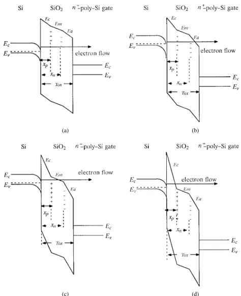
The interface states and oxide traps will be generated by hot electrons through breaking the weak bonds at the Si/SiO interface and the weak spots in the oxide. If the gate-oxide current is large enough, not only the latent oxide traps and Si/SiO interface states could be released but also the extra oxide traps and interface states could be generated. Due to the existence of electron traps and hole traps in the gate oxide, the potential distribution in the gate oxide will be perturbed and this will then influence the gate current in the next lapse. The potential distribution in the gate oxide is shown in Fig. 2.
It is shown that the hole traps would lower the potential near the cathode and the electron traps would raise the potential near the anode. Therefore, by Gauss’s Law the electric fields across the oxide are expressed as [15], [16]
(8) (9) (10)
(a) (b)
(c) (d)
Fig. 2. The MOS energy diagrams showing the existence of electron traps and hole traps.
Note that the image-force lowering effect on the barrier height is also considered. The FN tunneling current density across the potential barriers shown in Fig. 2(a)–(d) has the following form:
(11) and the tunneling probability for Fig. 2 can be calculated by using the WKB approximation in [14].
We assume that and are equal to zero at initial, i.e., the test samples were annealed, could be determined by solving (4)–(11). Once is determined, and can be resolved by using the electron trapping model [15], [17]
(12) The density of the trapped holes near the cathode is given by (13)
where the multiplication factor in the weak area can be expressed as
(14) and the impact ionization coffcient has the following form:
(15)
Note that MV/cm and at room
temper-ature [15]. The interface-state density can also be determined by the first-order kinetics
(16) As , and are determined, is then resolved in the next lapse from (4) to (11), and so on and so forth. The sur-face potential and the gate-oxide current of the wafer exposed in nonuniform plasma ambient could then be calculated during plasma processing. The rest of parameters used are listed in Table I. Some parameters listed in Table I are selected to be the same as previous papers [12], [16]. The ion current density is measured by using probe technique [12]. The photoresist was
(a) (b)
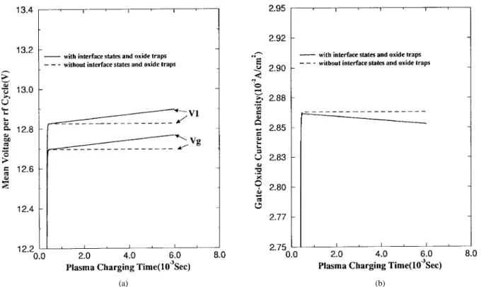
Fig. 3. (a) The mean voltage per rf cycle during plasma ashing process. (b) The mean gate-oxide current density per rf cycle during plasma ashing process. TABLE I
THEPARAMETERSUSED INOUR MODEL
removed by plasma asher in our studies and the RF power of this asher is 400 W. Note that the plasma damage of ashing process is significant in the overetch step rather than main step, owing to the large exposed area of polysilicon pad in plasmas.
IV. RESULTS AND DISCUSSION
As the fabricated wafers are exposed in plasma ambient, these wafer surfaces are charged by plasma charging current initially, and then the wafer surface potential will rise and it will shrink the plasma sheath, in turn lowering the plasma charging current. Furthermore, due to the increasing potential of the wafer, the gate-oxide current would increase. While the gate-oxide current is equal to the plasma charging current, the wafer surface potential will be saturated as the gate-oxide current. The simulated gate voltage and gate-gate-oxide
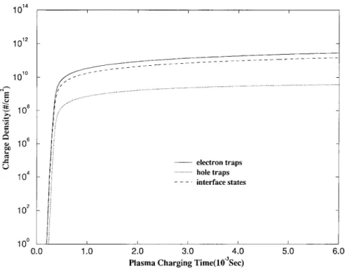
current are shown in Fig. 3(a)–(b). The gate-oxide current density will gradually decrease due to accumulated trapped electrons during cycle by cycle. However, the potential across the oxide will gradually increase (making the slight damage) and becomes constant (steady state, making the most serious damage due to the largest electric field) during the plasma current charging in each cycle. Therefore, the plasma-induced damage is almost caused by the steady-state charging current in each cycle and the used steady-state value is acceptable. The gate-oxide current density shown in Fig. 3 is the steady-state value for each cycle and the transient behavior isn’t shown in this figure. The electron traps, hole traps and interface states generated during plasma process are shown in Fig. 4. From Fig. 4, one can see that there exist a large number of generated electron traps. These oxide-trapped electron charges would impede gate-oxide current passing through oxide further and cause the gate-oxide current decrease, as shown in Fig. 3(b). To reach the saturation condition (i.e., the plasma charging current gate-oxide current), the potential across the gate oxide ( ) should increase further to force electrons passing through the gate oxide.
To correlate the simulated results with the measured results, the following experiment was performed. To release the latent gate oxide traps and Si/SiO interface states, the constant-current stress with constant-current density of 1 mA/cm and stress time of 1200 s is used. The n-channel MOSFET’s with four antenna ratios (10, 100, 400, 1000) are measured. The gate-oxide thickness is 14 nm, the channel width is 5 m, the channel length is 0.8 m, and the substrate resistivity is about 2.5–3.5 cm. To characterize the released gate oxide traps and Si/SiO interface states, the charge-pumping method is adopted. The curves of interface states versus different antenna ratios are shown in Fig. 5, in which the strong
Fig. 4. The electron/hole traps in the oxide and Si/SiO2 interface states generated during plasma ashing process.
Fig. 5. The correlation of the simulated oxide current density to the measured latent interface-state density for diffferent antenna ratios, and the synthetic guideline for predicting the gate oxide reliability from our simulated results.
correlation of the calculated time-averaged oxide current to measured Si/SiO interface states is obvious with a constant fitting number of about Therefore, the proposed physical model could provide the design rules for layout designer. For example, one can measure the interface states and obtain the correlation curve between antenna ratio and latent interface states. The simulated time-averaged gate-oxide current is then fitted and the fitting parameter is obtained. The critical interface states can then be extrapolated, and the
critical antenna ratio is obtained. The synthetic guideline is indicated in Fig. 5. Note that the critical interface-states is defined as one which causes 10% degradation of MOS device transconductance. From Fig. 5, if the effect of feedback on interface states and trapped electrons is not taken into account, the critical antenna ratio would be underestimated due to the overestimated gate-oxide current density. Therefore, the feedback effect should be taken into consideration for the accurate prediction of the critical antenna ratio.
Fig. 6. The simulated gate-oxide current densities related to different antenna ratios for different ion densities.
Fig. 7. The simulated gate-oxide current densities related to different antenna ratios for different plasma uniformities.
Moreover, the dependences of different process parameters on gate-oxide current and plasma-induced oxide damage are investigated, which include plasma ion density, plasma unifor-mity, gate-oxide thickness, and substrate doping concentration. A. Plasma Ion Density
While the MOS device is scaled down to the deep submicron era, plasma ion density needs to be increased to delineate
fine line pattern. According to the simulated results shown in Fig. 6, the gate-oxide current would increase if plasma ion density increases. Note that the plasma uniformity, i.e., , is maintained to be constant, and the only change is the plasma density. Therefore, damage due to plasma process used in VLSI manufacturing becomes more serious and how to eliminate this damage also becomes more important.
(a) (b)
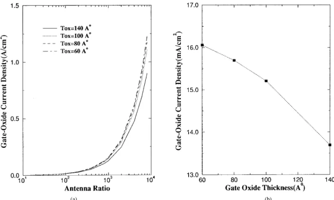
Fig. 8. (a) The simulated gate-oxide current densities related to different antenna ratios for different gate-oxide thicknesses. (b) The gate-oxide current density related to the gate oxide thickness. The antenna ratio used is 100.
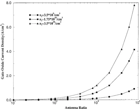
Fig. 9. The simulated gate-oxide current densities related to different antenna ratios for different substrate doping concentrations.
B. Plasma Uniformity
Plasma process-induced oxide damage occurs only in nonuniform plasma ambient, and different plasma uniformities cause different degrees of damage. We define plasma uniformity as and observe the relationship between plasma damage and plasma uniformity. Note that the electron density is assumed to be constant, and the plasma ion density is
changed. As shown in Fig. 7, the plasma uniformity influences the gate-oxide current significantly. How to maintain plasma uniformity of the etcher/asher becomes very important.
C. Gate-Oxide Thickness
As the gate-oxide thickness is scaled down, the simulated oxide current during plasma processing becomes larger, as
plasma processing. One can see that the gate-oxide voltage is about 8–16 V, depending on the gate-oxide thickness, and the sum of the voltage across the substrate depletion capacitor and the substrate is merely 1–2 V. Therefore, the variation of substrate doping concentration only slightly affects the change of plasma damage.
From our model, not only the plasma ion density but also the plasma uniformity play a major role in causing the plasma-induced oxide damage. The effect of gate-oxide thickness in causing the plasma-induced oxide damage would be saturated while the gate-oxide thickness is scaled. The surface poten-tial variation due to substrate doping concentration variation during plasma processing is small, and the variation very slightly affects the gate-oxide current. Therefore, in addition to improving the plasma process [18], [19], realizing uniform plasma ambient is the major issue in reducing the plasma process-induced oxide damage.
V. CONCLUSION
The plasma ashing process-induced oxide damage has been extensively studied. In our models, the gate-oxide current density, interface-state and oxide-trapped charges can be accu-rately calculated by considering the feedback effects, the sub-strate resistance and the flatband voltage. Owing to the correct calculation of interface-state and oxide-trapped charges, the devices fabricated in plasma ambient can be well-characterized prior to breakdown. Moreover, the influences of some param-eters adopted in deep submicron fabrication are also investi-gated and the trends are presented. Therefore, our simulator is useful in accurately predicting the plasma ashing process-induced damage.
REFERENCES
[1] Y. Kawamoto, “MOS gate insulator breakdown caused by exposure to plasma,” in Proc. 7th Symp. Dry Proc., 1985, p. 132.
[2] T. Namura and H. Uchida, “Charge build-up mechanism in barrel reactor,” in Proc. 11th Symp. Dry Proc., 1989, p. 74.
[3] M. Kubota, K. Harafuji, A. Yamano, H. Nakaga, and N. Normura, “Sim-ulational study for gate oxide breakdown mechanism due to nonuniform electron current flow,” in IEDM Tech. Dig., 1991, p. 132.
[4] S. Samukawa, “The charge built-up in an ECR plasma etching,” in Ext.
Abstr. 38th Meet., Jpn. Soc. Appl. Phys., 1991, p. 2499.
[5] I.-W. Wu, M. Koyanagi, S. Holland, T. Y. Huang, J. C. Mikkelsen, Jr., R. H. Bruce, and A. Chiang, “Breakdown yield and lifetime of thin gate oxide in CMOS processing,” J. Electrochem. Soc., vol. 136, p. 1638, 1989.
[6] W. M. Green, J. B. Kruger, and G. Kooi, “Magnetron etching of polysilicon: Etching damage,” J. Vac. Sci. Technol. B, 1991, p. 366.
down from gate charging during resist ashing,” IEEE Trans. Electron
Devices, vol. 41, p. 1848, 1994.
[13] B. Chapman, Glow Discharge Process. New York: Wiley, 1980, p. 51. [14] K. Hashimoto, “Charge damage caused by electron shading effect,” Jpn.
J. Appl. Phys., 1994, p. 6013.
[15] I. C. Chen, S. E. Holland, and C. Hu, “Electrical breakdown in thin gate and tunneling oxides,” IEEE Trans. Electron Devices, vol. ED-32, p. 413, 1985.
[16] C.-F. Chen and C.-Y. Wu, “Transport properties of thermal oxide films grown on polycrystalline silicon—Modeling and experiments,” IEEE
Trans. Electron Devices, vol. ED-34, pp. 1590, 1987.
[17] , “The dielectric reliability of intrinsic thin SiO2films thermally grown on a heavily doped Si substrate—Characterization and modeling, ” IEEE Trans. Electron Devices, vol. ED-34, p. 1540, 1987.
[18] K.-F. You and C.-Y. Wu, “A novel two-step etching process for reducing plasma-induced oxide damage,” Solid-State Electron., vol. 39, no. 5, p. 689, 1996.
[19] C. T. Gabriel and M. G. Weling, “Gate oxide damage reduction using a protective dielectric layer,” IEEE Electron Device Lett., vol. 15, p. 269, 1994.
Kuo-Feng You (S’91) was born in I-Lan,
Tai-wan, R.O.C., on August 12, 1969. He received the B.S. degree from the Department of Electron-ics Engineering, National Chiao-Tung University (NCTU), Hsinchu, Taiwan, in 1991. He is cur-rently pursuing the Ph.D. degree in the Institute of Electronics at NCTU. His research areas focus on deep-submicrometer MOS device physics and reliability issues, especially the gate oxide damage from plasma-induced wafer charging.
Ming-Chien Chang was born in Tao-Yuan, Taiwan,
R.O.C., on September 5, 1956. He received the B.S. degree in physics from National Hsin-Hua University, Hsinchu, Taiwan, and the M.S. degree from the Institute of Electronics, National Chiao-Tung University (NCTU), Hsinchu, Taiwan, in 1979 and 1981, respectively. Currently, he is a Ph.D. candidate at NCTU.
From 1982 to 1984, he was an Assistant Researcher in the Telecommunications Laboratory, Tao-Yuan, working on thin-film and thick-film components, and hybrid integrated circuits. From 1984 to 1994, he was with the Electronic Research and Service Organization (ERSO), ITRI, Hsinchu, where he worked in the area of CMOS process, device design, process and device reliability in the SRAM and DRAM technology. Since 1994, he has been with Vanguard International Semiconductor Corporation, Hsinchu, as a Manager of deep submicron device design and reliability in advanced DRAM technology.
Ching-Yuan Wu (S’72–M’75), for a photograph and biography, see this issue,