472 IEEE ELECTRON DEVICE LETTERS, VOL. 22, NO. 10, OCTOBER 2001
A Novel High-Performance Poly-Silicon Thin Film
Transistor With a Self-Aligned Thicker Sub-Gate
Oxide Near the Drain/Source Regions
Kow Ming Chang, Yuan Hung Chung, Gin Ming Lin, Jian Hong Lin, and Chi Gun Deng
Abstract—In this letter, a novel high-performance poly-silicon
thin-film transistor (poly-Si TFT) with a self-aligned thicker sub-gate oxide near the drain/source regions is proposed. Poly-Si TFTs with this new structure have been successfully fabricated and the results demonstrate a higher on-off current ratio of
5 9 106and also shows the off-state leakage current 100 times
lower than those of the conventional ones at GS = 15 V
and DS = 10 V. Only four photo-masking steps are required
and fully compatible with the conventional TFT fabrication processes. This novel structure is a good candidate for the further high-performance large-area device applications.
Index Terms—On–off current ratio, photo-masking steps,
poly-silicon thin-film transistor, self-aligned thicker sub-gate oxide.
I. INTRODUCTION
P
OLY-SILICON thin-film transistors (poly-Si TFTs) have received increasing attention for high-performance large-area active matrix liquid crystal display (AMLCD) applications as compared to conventional amorphous-Si TFTs [1], [2]. However, the undesired off-state leakage current for a poly-Si TFT is much higher than that of an amorphous-Si TFT. It has been reported that the conduction mechanism for the off-state leakage current is the field emission via grain boundary traps due to high electric field in the drain depletion region [3]. Thus, to reduce the drain electric field, suppressing the off-state leakage current is required. Several methods have been proposed to achieve this purpose, such as offset gated structure [4], lightly doped drain structure [5] and field induced drain structure [6], [7]. The implant damage in the lightly doped offset drain structure can cause an undesired degradation in the drain junction, especially for low-temperature processed poly-Si TFTs [8]. In the field induced drain structure, an additional photo masking step is required and unavoidable photo masking misalignment error will occur [6], [7].In this letter, we propose a novel TFT structure with a self-aligned thicker sub-gate oxide near the drain/source regions which has a much lower off-state leakage current and higher on-off current ratio than those of a conventional structure. Only four photo-masking steps are required and it is
Manuscript received June 7, 2001; revised July 27, 2001. This work was supported by the National Science Council of Taiwan, R.O.C. under Contract NSC89-2215-E009-089. The review of this letter was arranged by Editor T.-J. King.
The authors are with the Department of Electronics Engineering and Insti-tute of Electronics of National Chiao-Tung University, Hsinchu, 300, Taiwan, R.O.C. (e-mail: [email protected])
Publisher Item Identifier S 0741-3106(01)08861-9.
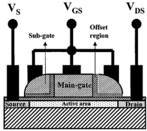
Fig. 1. Schematic diagram of the proposed new TFT structure.
fully compatible with the conventional TFT processes. Poly-Si TFTs with the new structure are successfully demonstrated.
II. EXPERIMENTS
Fig. 1 shows the schematic diagram of the proposed TFT structure. The top view of the proposed TFT structure is shown in Fig. 2(a) and the cross-sectional view along the line AA’ is shown in Fig. 2(b). A conventional top gate TFT structure was formed with 200-nm poly-Si active layer, 50-nm plasma enhanced chemical vapor deposition (PECVD) gate oxide layer deposited at 350 C, 400-nm poly-Si main gate electrode and 10 m channel length. The 200-nm poly-Si active layer is formed by silicon amorphous layer deposition in low pressure chemical vapor deposition (LPCVD) system using Si H gas at 460 C and then crystallized at 600 C for 24 h. The average grain size measured by transmission electron microscopy and the trap state density determined using Levinson’s method [9] are 1.1 m and cm , respectively. After main gate electrode patterning and blanket deposition of 100-nm PECVD oxide and 350-nm poly-Si layers, a reactive ion etching process was used to anisotropically etch the poly-Si and PECVD oxide layers. Therefore, self-aligned offset region (PECVD oxide) and self-aligned poly-Si spacers were formed [Fig. 2(b)]. The self-aligned poly-Si spacers are also noted as the sub-gates of the TFT. The gate oxide for the sub-gate region with length 300 nm is thicker than the main-gate region and is almost 150 nm. For n-channel transistors, P implant with a dosage of at 40 KeV was used and then activated in at 600 C for 24 h. To apply the voltage source on the sub-gates, new contact windows were opened as shown in Fig. 2(c), which
CHANG et al.: NOVEL HIGH-PERFORMANCE POLY-SILICON THIN FILM 473
Fig. 2. (a) Top view of the proposed TFT structure. (b) Cross-sectional view along the line AA’. (c) Cross-sectional view along the line BB’.
is the cross-section BB’. Poly-Si TFTs with conventional structure, e.g., without the sub-gates, were also fabricated to serve as a control. The channel length of the proposed TFT ( m) is the summation of the main gate length (10 m), the thickness of two self-align offset PECVD oxides (0.2 m) and the length of the two sub-gate lengths (0.6 m).
It should be mentioned here that the current-voltage (I-V) characteristics of the proposed TFT have not been optimized be-cause the electric characteristics are very sensitive to the length of the sub-gate. The study of the optimization of the sub-gate length for the proposed TFT structure is still under investiga-tion.
III. RESULTS ANDDISCUSSION
As shown in Fig. 3, the off-state leakage current of the new TFT is much lower than that of the conventional TFT control. The off state leakage current at V is 100 times smaller than that of the conventional TFT control ( m). The on-off current ratios of the conventional and proposed TFTs are and , respectively. The on-off current ratio is defined as that ratio of the maximum on state current to the minimum off– state current. The main reason for much lower off-state leakage current of the new TFT is that the drain electric field is greatly reduced for the thicker gate oxide in the sub-gate regions and the self-aligned offset PECVD oxide. The
Fig. 3. I 0V transfer characteristics of the conventional and new TFTs.
Fig. 4. I 0V characteristics of the conventional and proposed TFTs.
characteristics of a short channel device ( m) are also shown in Fig. 3. It can be observed that the leakage cur-rent improvement in the short channel device is not as good as in the long channel device. This is because the electric field in a short channel device is so high that it is not easy to reduce the electric field and make the decreasing of leakage current ef-fectively. In Fig. 4, less kink effect can be observed in the new TFT to further confirm that the drain electric field can be ef-fectively reduced in the proposed TFT. Although the off-state leakage current can be reduced, the turn-on current is slightly degraded due to the higher source/drain series resistance caused by the thicker sub-gate oxide and the self-aligned offset PECVD oxide. The optimization of the sub-gate length is still under in-vestigation to have an acceptable series resistance for on-state and off-state characteristics.
IV. CONCLUSION
In this letter, a novel high-performance TFT with a self-aligned thicker sub-gate oxide near the drain/source regions has been proposed and successfully demonstrated. Much lower off-state leakage currents and a higher on-off
474 IEEE ELECTRON DEVICE LETTERS, VOL. 22, NO. 10, OCTOBER 2001
current ratio can be obtained for the proposed TFT. The TFT fabrication processes are fully compatible with the conventional four-mask ones. This new TFT structure may be an attractive device structure for future high-performance large-area device applications.
REFERENCES
[1] I. W. Wu, “Low temperature poly-Si TFT technology for AMLCD ap-plication,” in Tech. Dig. AM-LCD, 1995, pp. 7–10.
[2] , “Poly-Si TFT LCD technology and prospect of further displays,” in Tech. Dig. EDMS, 1997, pp. 309–312.
[3] J. G. Fossum, A. Ortiz-Conde, H. Shichijo, and S. K. Banerjee, “Anoma-lous leakage current in LPVCD polysilicon MOSFET’s,” IEEE Trans. Electron Devices, vol. ED-32, pp. 1878–1884, Sept. 1985.
[4] J. I. Han and C. H. Kan, “A self-aligned offset polysilicon thin-film tran-sistor using photoresist reflow,” IEEE Electron Device Lett., vol. 20, pp. 476–477, Sept. 1999.
[5] P. S. Shih, C. Y. Chang, T. C. Chang, T. Y. Huang, D. Z. Peng, and C. F. Yeh, “A novel lightly doped drain polysilicon thin-film transistor with oxide sidewall spacer formed by one-step selective liquid phase deposi-tion,” IEEE Electron Device Lett., vol. 20, pp. 421–423, Aug. 1999. [6] T. Y. Huang, I. W. Wu, A. G. Lewis, A. Chiang, and R. H. Bruce, “Device
sensitivity of field-plated high-voltage TFT’s and their application to low-voltae operation,” IEEE Electron Device Lett., vol. 11, pp. 541–543, Nov. 1990.
[7] K. Tanaka, K. Nakazawa, S. Suyama, and K. Kato, “Characteristics of field-induced-drain (FID) poly-Si TFT’s with high on/off current,” IEEE Trans. Electron Devices, vol. ED-39, pp. 916–920, April 1992. [8] K. Y. Choi and M. K. Han, “A novel gate-overlapped LDD poly-Si thin
film transistor,” IEEE Electron Device Lett., vol. 17, pp. 566–568, Dec. 1996.
[9] J. Levinson, F. R. Shepherd, P. J. Scanlon, W. D. Westwood, G. Este, and M. Rider, “Conductivity behavior in polycrystalline semiconductor thin film transistors,” J. Appl. Phys., vol. 53, pp. 1193–1202, 1982.