Multilayer polymer light-emitting diodes by blade coating method
Shin-Rong Tseng, Hsin-Fei Meng, Kuan-Chen Lee, and Sheng-Fu Horng
Citation: Applied Physics Letters 93, 153308 (2008); doi: 10.1063/1.2999541
View online: http://dx.doi.org/10.1063/1.2999541
View Table of Contents: http://scitation.aip.org/content/aip/journal/apl/93/15?ver=pdfcov Published by the AIP Publishing
Articles you may be interested in
Solution processed multilayer polymer light-emitting diodes based on different molecular weight host J. Appl. Phys. 109, 074516 (2011); 10.1063/1.3569831
Multilayer green polymer light emitting diodes with improved efficiency and lifetime J. Appl. Phys. 100, 034506 (2006); 10.1063/1.2229439
Efficient polymer white-light-emitting diodes
Appl. Phys. Lett. 86, 163502 (2005); 10.1063/1.1901824
Efficient and stable blue lightemitting diodes based on an anthracene derivative doped poly( N -vinylcarbazole)
Appl. Phys. Lett. 85, 5433 (2004); 10.1063/1.1823585
Color-tunable multilayer light-emitting diodes based on conjugated polymers Appl. Phys. Lett. 84, 1195 (2004); 10.1063/1.1645983
This article is copyrighted as indicated in the article. Reuse of AIP content is subject to the terms at: http://scitation.aip.org/termsconditions. Downloaded to IP: 140.113.38.11 On: Wed, 30 Apr 2014 22:52:04
Multilayer polymer light-emitting diodes by blade coating method
Shin-Rong Tseng,1Hsin-Fei Meng,1,a兲Kuan-Chen Lee,2and Sheng-Fu Horng31Institute of Physics, National Chiao Tung University, Hsinchu 300, Taiwan
2Institute of Electronic Engineering, National Chiao Tung University, Hsinchu 300, Taiwan 3Department of Electrical Engineering, National Tsing Hua University, Hsinchu 300, Taiwan
共Received 10 February 2008; accepted 10 September 2008; published online 17 October 2008兲 Multilayer polymer light-emitting diodes fabricated by blade coating are presented. Multilayer of polymers can be easily deposited by blade coating on a hot plate. The multilayer structure is confirmed by the total thickness and the cross section view in the scanning electron microscope. The film thickness variation is only 3.3% in 10 cm scale and the film roughness is about 0.3 nm in the micron scale. The efficiency of single layer poly共para-phenylene vinylene兲 copolymer Super Yellow and poly共9,9-dioctylfluorene兲 共PFO, deep blue兲 devices are 9 and 1.7 cd/A, respectively, by blade coating. The efficiency of the PFO device is raised to 2.9 cd/A with a 2-共4-tert-butylphenyl兲-5-共4-biphenylyl兲-1,3,4-oxadiazole 共PBD兲 hole-blocking layer and to 2.3 cd/A with a poly关共9,9-dioctylfluorenyl-2,7-diyl兲-co-共4,4
⬘
-共N-共4-sec-butylphenyl兲兲diphenylamine兲兴 elec-tron-blocking layer added by blade coating. © 2008 American Institute of Physics.关DOI:10.1063/1.2999541兴
Small molecule organic light-emitting diodes 共OLEDs兲 and polymer light-emitting diodes 共PLEDs兲 have generated great interest in the past decade. Due to its low cost solution process PLED has the potential to be more competitive than OLED in many future applications.1–3It can be applied in the lighting for interior design, clothes, purses, cars, and even the art works. The most common fabrication process for PLED is spin coating. However, the usage of materials is only 5% and the manufacturing throughput by spin coating is low for large areas, raising dramatically the cost of PLED. More importantly, it has been proved difficult to make multilayer polymer structures by spin coating because the solvent of the second layer will dissolve the first. The multilayer structure including carrier transport, emission, and carrier blocking layers is known to be necessary for high efficiency. The incompatibility between spin coating method and multilayer device design is the main reason that the per-formance of PLED is so far below that of the thermally evaporated OLED. In the past few years many strategies were developed to overcome the dissolution problem and make multilayer PLEDs by spin coating.4–9 A liquid buffer method which completely prevents the dissolution was re-cently reported to achieve high-efficiency and stable PLEDs.10Material waste is, however, still a problem and it is nontrivial to scale up to very large areas. Blade coating is a common method to form large-area polymer films with mi-crometer thickness such as photoresists and color filters.11 Unlike spin coating the area can be easily scaled up and the material usage is almost 100%. Furthermore, not only single layer but also multilayer can be deposited without a buffer liquid. The single layer PLED performance is as good as that of the spin coated one. The bilayer PLED is even better than the one by liquid buffer method.
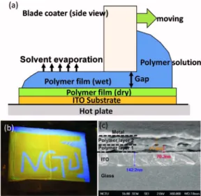
The working principle of multilayer fabrication process by blade coating is shown in Fig.1共a兲. A heater is needed for multilayer process to expel the solvent of the second polymer solution. So the second film is formed by solution but
quickly dried before dissolving the first polymer layer. A 70 nm poly共para-phenylene vinylene兲 copolymer Super-Yellow 共S-Y, supplied by Merck OLED Materials GmbH兲 thin film was first formed by blade coating in toluene solu-tion with a scratch pattern “NCTU” made by a cotton stick with solvent 共toluene兲. Then poly共9,9-dioctylfluorene兲 共PFO, purchased from American Dye Source兲 solution was blade coated on top of the S-Y layer to form a 70 nm thin film. The sample was placed on a 70 ° C hot plate as the second layer was blade coated for rapid solvent evaporation. The total thickness of the S-Y/PFO bilayer was 150 nm as measured by a Kosaka ET4000 surface profiler, which was the same as the sum of the thickness of the individually blade coated S-Y and PFO layers. The NCTU pattern of the first S-Y layer is not damaged by the second PFO solution at all as shown in Fig. 1共b兲 under ultraviolet illumination, implying that the
a兲Author to whom correspondence should be addressed. Electronic mail:
FIG. 1. 共Color online兲 共a兲 Schematic working principle of multilayer struc-ture by blade coating; the process of the second layer is on a hot plate. The solvent of the second layer is quickly evaporated without dissolving the first layer.共b兲 Double layer S-Y/PFO under ultraviolet illumination. The scratch pattern NCTU is made by a cotton stick on the S-Y thin film before blade coating the PFO thin film.共c兲 The lateral profile of the double layer polymer film by SEM. There is no dissolution between these two polymer layers by blade coating.
APPLIED PHYSICS LETTERS 93, 153308共2008兲
0003-6951/2008/93共15兲/153308/3/$23.00 93, 153308-1 © 2008 American Institute of Physics
This article is copyrighted as indicated in the article. Reuse of AIP content is subject to the terms at: http://scitation.aip.org/termsconditions. Downloaded to IP: 140.113.38.11 On: Wed, 30 Apr 2014 22:52:04
mutual dissolution is minimal. The pattern will be com-pletely destroyed if the PFO layer is deposited by spin coat-ing. The lateral profile was checked by scanning electron microscope共SEM, JEOL JSM-6390LV兲. The result is shown in Fig. 1共c兲. It is clear that there exists an interface between the two polymer layers. The uniformity was verified by com-parison with the standard spin coated films. The large scale uniformity in an area of 6⫻5 cm2 is 60⫾3 nm for spin
coating, 60⫾2 nm for blade and spin coating, and 60⫾10 nm for blade coating on a hot plate at 70 °C. The polymer film roughness in a 0.5⫻1m2 area is 5.5 Å for spin coating, 3.6 Å for blade and spin coating, and 3.1 Å for blade coating on a hot plate. The single layer polymer thin film by blade coating is almost the same as that by spin coating in both macroscopic and microscopic scales. Blade coating therefore combines the advantages of multilayer deposition and efficient material usage without sacrificing the film quality.
Now we turn to PLED performance. Single layer PLEDs of the structure ITO/FEDOT:PSS/EML/CsF/Al were fabricated. PEDOT:PSS is poly-共3,4-ethylenedioxy-thiophene兲:poly-共styrenesulfonate兲. S-Y and PFO were used for the emissive layer 共EML兲. Both S-Y and PFO were dissolved in toluene. Bilayer PFO devices were made with the structures ITO/PEDOT:PSS/TFB/PFO/CsF/Al and ITO/PEDOT/PFO/PBD/CsF/Al. TFB is poly关共9,9-di-octylfluorenyl-2,7-diyl兲-co-共4,4
⬘
-共N-共4-sec-butylphenyl兲兲di-phenylamine兲兴 purchased from American Dye Source. PBD is 2-共4-tert-butylphenyl兲-5-共4-biphenylyl兲-1,3,4-oxadiazole purchased from Sigma Aldrich. TFB acts as the electron blocking layer and PBD as the hole blocking layer. Both TFB and PBD were dissolved in toluene. The indium tin oxide 共ITO兲 substrates were cleaned and the surfaces were treated by oxygen plasma followed by spin coating 50 nm of PEDOT:PSS. The PEDOT:PSS film was baked at 200 ° C for 5 min in vacuum environment 共10−3torr兲. The TFB film 共30 nm兲 was spin coated on the PEDOT:PSS film and an-nealed at 180 ° C in vacuum for 40 min. PFO was blade coated on top of the TFB layer on a hot plate at 70 ° C. PBD was blade coated on the PFO layer on a hot plate at 100 ° C. The thickness of PFO is about 80 nm in single layer devices and 70 nm in bilayer devices. S-Y was blade coated on PE-DOT:PSS. The PFO and S-Y thin film were annealed at 120 ° C in vacuum 共10−3 torr兲. All the devices were coatedwith CsF共2 nm兲/Al共100 nm兲 cathode and packaged in a glove box.
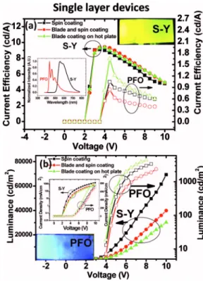
Figure 2 shows the results of single layer devices. The values of the maximum efficiency of S-Y PLEDs are almost the same 共about 9 cd/A at 3.5 V兲. Surprisingly the perfor-mance of PFO PLED by blade coating on a hot plate is the best. Since the uniformity is almost the same for all PFO films, we speculate that the chain entanglement of PFO in the nanometer scale by blade coating on a hot plate is stronger than that of the other methods. Such entanglement enhance-ment is important for the low molecular weight 共MW兲 PFO 共MW below 100 000兲 but not so for the high MW S-Y 共MW about 1 000 000兲.12
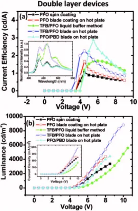
Bilayer PFO devices with structures of TFB/PFO and PFO/PBD were made by blade coating on a hot plate for the second layer. The results are shown in Fig.3. The maximum efficiency is raised to 2.3 cd/A for TFB/PFO as compared to 1.05 cd/A for the single layer PFO device. The TFB/PFO
made by liquid buffer has the efficiency of 1.7 cd/A which is lower than that of the same structure made by blade coating. This is probably because TFB and PFO are more in contact with each other in blade coating on a hot plate than in the liquid buffer process. Moreover the device efficiency is raised to 2.9 cd/A in the PFO/PBD device. The maximum luminance is 8807 cd/m2for the TFB/PFO device, about 2.5
times larger than that of the single layer PFO device 共3371 cd/m2兲. The maximum luminance is 4429 cd/m2 for
the PFO/PBD device. The enhancement in the TFB/PFO bi-layer devices is due to the fact that the electrons in PFO are blocked by TFB, which induces more holes to be injected and achieves higher efficiency and luminance. As for the PFO/PBD device the holes are blocked by PBD. The effi-ciency is enhanced by separating the recombination zone from the cathode to reduce metal quenching.
The basic transport and optical properties of films by various fabrication methods are investigated by the currents in hole-only and electron-only devices and by comparing the photoluminescence 共PL兲 spectra. The structures are ITO/PEDOT/EML/Al for hole-only devices and Al/EML/ CsF/Al for electron-only devices. The results are shown in Fig. 4. The electron currents of the blade coated and spin coated devices are almost the same. Due to the Ohmic contact with CsF/Al cathode the electron current follows space-charge-limited current behavior, JSCLC=共9/8兲e关共V − Vbi兲2/L3兴. J is the current density, is the
permit-tivity of the polymer, e is the electron mobility, V is the driving voltage, Vbi is the built-in voltage, and L
is the polymer thickness. The fitted electron mobility is 2.5⫻10−8cm2/V s for PFO 共at 0.6 MV/cm兲 and 5
FIG. 2. 共Color online兲 Device performance of single layer S-Y and PFO PLEDs by spin coating共square兲, blade and spin coating 共circle兲, and blade coating on a hot plate 共triangle兲. 共a兲 The current efficiency. Inset is the electroluminescent spectra of S-Y and PFO devices by blade coating as well as the S-Y device in operation. The active area of the device is 4⫻7.5 cm2.共b兲 The luminance. Inset is the current density and the PFO
device by blade coating in operation. The active area of the device is 4⫻7.5 cm2.
153308-2 Tseng et al. Appl. Phys. Lett. 93, 153308共2008兲
This article is copyrighted as indicated in the article. Reuse of AIP content is subject to the terms at: http://scitation.aip.org/termsconditions. Downloaded to IP: 140.113.38.11 On: Wed, 30 Apr 2014 22:52:04
⫻10−6cm2/V s for S-Y 共at 0.6 MV/cm兲 with all fabrication
methods. Strictly speaking the space-charge-limited formula is valid only for trap-free cases. Although there may be some overall correction due to the traps on the absolute values of the electron mobility, the relative magnitudes of the mobility for the fabrication processes are still meaningful. Such re-sults provide the microscopic basis for the similarity in per-formances for blade and spin coated PLEDs. The hole cur-rents of the blade coated devices are slightly higher than those of the spin coated ones. Because of the large hole injection barrier the current is dominated by defect levels in the energy gap.13 The large hole current for blade coating may be due to the gap levels originated from the aggregates. In PLED the hole injection is no longer limited by the high barrier due to the higher field near the anode;13the aggregate levels may cause lower hole mobilities and lower luminances in blade coated PLED. However, in the PL spectra of PFO films, the shoulder peaks of 464 and 494 nm grow in blade coated films which may contain more aggregates and there-fore stronger low energy emission due to exciton delocalization.14
In conclusion we have developed a way to simulta-neously reduce the cost of PLED and prevent the dissolution between two polymer layers by blade coating. This is a very simple method to fabricate all-solution-processed multilayer polymer devices in potentially very large areas up to meter scales. The film uniformity is about the same as standard spin coated films in both large and small scales. The perfor-mance of the single layer PLED by blade coating is the same as that of spin coated ones. For bilayer PLED made by blade coating the efficiency is more than double compared with the single-layer spin coated PLED.
S.R.T. and H.F.M. would like to thank Dr. Sunny Duan in Material and Chemical Research Laboratories, Industrial Technology Research Institute in Taiwan for stimulating dis-cussions. The authors thank the Merck OLED Materials GmbH for supplying the S-Y polymer. This work is sup-ported by the National Science Council of Taiwan under Grant Nos. NSC 96-2112-M-009-036 and NSC 96-2120-M-007-007.
1T. Y. Cho, C. L. Lin, and C. C. Wu,Appl. Phys. Lett. 88, 111106共2006兲. 2J. Huang, G. Li, E. Wu, Q. Xu, and Y. Yang,Adv. Mater.共Weinheim, Ger.兲
18, 114共2006兲.
3T. W. Lee, M. G. Kim, S. Y. Kim, S. H. Park, O. Kwon, and T. Noh,Appl.
Phys. Lett. 89, 123505共2006兲.
4G. K. Ho, H. F. Meng, S. C. Lin, S. F. Horng, C. S. Hsu, L. C. Chen, and
S. M. Chang,Appl. Phys. Lett. 85, 4576共2004兲.
5Z. Liang and O. M. Cabarcos, Adv. Mater. 共Weinheim, Ger.兲 16, 823
共2004兲.
6W. Ma, P. K. Iyer, X. Gong, B. Liu, D. Moses, G. C. Bazan, and A. J.
Heeger,Adv. Mater.共Weinheim, Ger.兲 17, 274共2005兲.
7J. S. Kim, R. H. Friend, I. Grizzi, and J. H. Burroughes,Appl. Phys. Lett.
87, 023506共2005兲.
8T. W. Lee, M. G. Kim, S. Y. Kim, S. H. Park, O. Kwon, T. Noh, and T. S.
Oh,Appl. Phys. Lett. 89, 123505共2006兲.
9D. K. Park, A. R. Chun, S. H. Kim, M. S. Kim, C. G. Kim, T. W. Kwon,
S. J. Cho, H. S. Woo, J. G. Lee, S. H. Lee, and Z. X. Guo,Appl. Phys. Lett. 91, 052904共2007兲.
10S. R. Tseng, S. C. Lin, H. F. Meng, H. H. Liao, C. H. Ye, H. C. Lai, S. F.
Horng, and C. S. Hsu,Appl. Phys. Lett. 88, 163501共2006兲.
11F. Davard and D. Dupuis, J. Non-Newtonian Fluid Mech. 93, 17共2000兲. 12H. Becker, H. Spreitzer, W. Kreuder, E. Kluge, H. Schenk, I. Paker, and Y.
Cao,Adv. Mater.共Weinheim, Ger.兲 12, 42共2000兲.
13C. K. Yang, C. M. Yang, H. H. Liao, S. F. Horng, and H. F. Meng,Appl.
Phys. Lett. 91, 093504共2007兲.
14D. Neher,Macromol. Rapid Commun. 22, 1365共2001兲.
FIG. 3.共Color online兲 Device performance of single layer PFO PLEDs and double layer TFB/PFO and PFO/PBD PLEDs.共a兲 The current efficiency. Inset is the electroluminescent spectra of the devices. The spectra of single layer PFO and double layer PFO/PBD devices are almost the same and normalized to 0.5 for clarity.共b兲 The luminance. Inset is the current density. Single layer PFO devices by spin coating共solid square兲 and by blade coat-ing on the hot plate 共empty square兲. Double layer TFB/PFO devices by liquid buffer method 共solid circle兲 and by blade coating on a hot plate 共empty circle兲. Double layer PFO/PBD device by blade coating on a hot plate共solid triangle兲.
FIG. 4. 共Color online兲 Hole-only and electron-only devices made by spin coating共square兲, blade and spin coating 共circle兲, and blade coating on a hot plate 共triangle兲. 共a兲 S-Y devices: 共b兲 PFO devices. Inset shows the PL spectra.
153308-3 Tseng et al. Appl. Phys. Lett. 93, 153308共2008兲
This article is copyrighted as indicated in the article. Reuse of AIP content is subject to the terms at: http://scitation.aip.org/termsconditions. Downloaded to IP: 140.113.38.11 On: Wed, 30 Apr 2014 22:52:04