Materials Chemistry and Physics 72 (2001) 236–239
Properties of Si–C–N films prepared on Si substrate
using cobalt interfacial layers
Hui Lin Chang, Cheng Tzu Kuo
∗Department of Materials Science and Engineering, National Chiao Tung University, 1001 Ta-Hsueh Road, Hsincho 300, Taiwan
Abstract
A microwave plasma chemical vapor deposition (MPCVD) process was successfully used to synthesize Si–C–N films. The film properties were tuned by deposition parameters and engineering interfacial Co layers on Si substrates. The films were deposited by using CH4, N2,
and additional solid Si columns as raw material sources. The films were characterized by scanning electron microscopy (SEM) for film morphologies, X-ray photo-emission spectroscopy (XPS) and cathodoluminescence (CL) spectroscopy for bonding structure and band gap analyses. The results show that the application of Co interlayer can have the following effects: (1) it can change film morphology from (1 0 0) preferred orientation to become pyramidal structure, and the band gap from 2.93 to 4.00 eV; (2) it may possess the additional Si(2p)–Si bonding in the films. By adding additional Si source, the atomic ratio of Si:C:N can change significantly with the decrease in carbon content of films, the film structure may vary from amorphous to crystalline and possess additional C(1s)≡N bonding (or N(1s)≡C bonding). In summary, the composition, morphology, bonding and crystal structures of Si–C–N films have been successfully demonstrated to be manipulated through applications of Co interlayer and additional Si source. © 2001 Elsevier Science B.V. All rights reserved.
Keywords: Nitrides; Plasma assisted CVD; X-ray photo-emission spectroscopy; Electron microscopy
1. Introduction
Carbon nitride and silicon carbon nitrides are predicted to exhibit many extraordinary properties including excellent field emission characteristic, highest hardness and semicon-ductor behavior [1–5]. Research in the synthesis of Si–C–N crystals is growing very rapidly. Much effort has been de-voted to increase the crystallinity and to control or tune the film properties. One of the methods for increasing the crystallinity was to add an additional source of Si either as gas phase or solid forms [1–3]. Application of interlayer to grow the oriented Si–C–N nanorods was reported [1], but the detailed bonding structures and compositions were not clear. The cobalt acting as a catalyst for carbon nan-otubes deposition and CH4decomposition was preliminar-ily reported [6,7]. The mechanisms on effect of interlayer application will be an interesting topic. The purpose of this paper was to examine the possibility to tune the Si–C–N film properties through applying interlayer between the Si–C–N films and silicon substrates in addition to changing the other process parameters.
∗Corresponding author. Tel.:+886-3-5731-949; fax: +886-3-5724-727. E-mail address: ctkuo@cc.nctu.edu.tw (C.T. Kuo).
2. Experimental
The Si–C–N films were prepared by a microwave plasma chemical vapor deposition (MPCVD) system using CH4 and N2 as source gases and with or without additional Si source. The substrate materials include p-type Si (1 0 0) wafers and wafers precoated with 1000 Å Co by a PVD process. The additional Si sources were added by inserting four Si chip columns in the sample holder at the symmetri-cal positions around the specimen. The process conditions were as follows: CH4/N2flow ratio = 10/100 sccm/sccm, microwave power = 800 W, total pressure = 12 Torr, substrate temperature= 1000–1200◦C.
The film compositions were determined by X-ray photo-emission spectroscopy (XPS) (Microteck MT-500). The scanning electron microscopy (SEM) was used to exam-ine the film morphologies. The band structures of the films were studied by cathodoluminescence (CL) spectroscopy.
3. Results and discussion
3.1. Film morphologies
The typical morphologies of the films deposited by adding additional Si source on Si wafer and Si wafer with 0254-0584/01/$ – see front matter © 2001 Elsevier Science B.V. All rights reserved.
H.L. Chang, C.T. Kuo / Materials Chemistry and Physics 72 (2001) 236–239 237
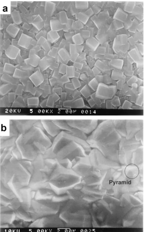
Fig. 1. The typical SEM morphology of the Si–C–N films: (a) films deposited on Si substrate with additional Si source; (b) films deposited on Co substrate with additional Si source.
Co interlayer are depicted in Fig. 1(a) and (b), respectively. Fig. 1(a) indicates a better uniformity in grain size with (1 0 0) preferred orientation, as contrasted to pyramidal structure in Fig. 1(b). In other words, the films on Si wafer with Co interlayer are expected to possess a higher specific surface area and so a higher efficiency in field emission.
Effect of adding additional Si source on film deposition can be examined by comparing Fig. 1(b) with Fig. 2 for films without additional Si source. It is noted that the structure of Fig. 2 is amorphous instead of pyramidal crystalline struc-ture in Fig. 1(b). Such a difference in film deposition may relate to the detrimental effect of Co in cemented carbides on diamond nucleation [8].
3.2. Film compositions
The average atomic ratios of the Si–C–N films derived from XPS analyses are shown in Table 1. The films were sputtered for 2 min by Ar ion to reduce possible
contamina-Fig. 2. The typical SEM morphology of the Si–C–N films deposited on Co/Si substrate without additional Si source.
tion before XPS analyses. The oxygen contents of the films are below 10 at.% and are omitted in Table 1 to elucidate the relative ratios between Si, C and N atoms. The samples A, B and C represent the same coating and substrate materials but different interlayer application and deposition conditions, in order to tune the properties of films. It is noted that appli-cation of Co interlayer has no significant effect on the film compositions, by comparing sample A with B. However, the films without additional Si source (sample C) appeal to in-crease carbon content significantly. The additional Si source can occupy additional space to dilute the carbon source in reaction chamber to reduce carbon deposition rate.
3.3. Bonding structures
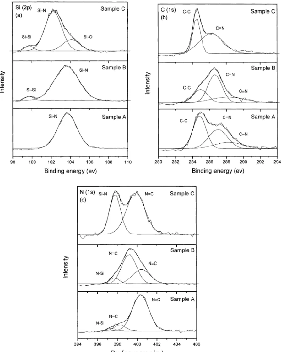
The XPS core level spectra of Si(2p) for samples A, B and C are shown in Fig. 3(a), where the monochromatic X-ray source is Mg K␣ line (1253.6 eV) with linewidth, 0.7 eV. The pass energy of 23.5 eV is used for spectra scan and the diameter of the analysis area is∼800 m. Through Gauss convolution analyses on XPS spectra, the common bonding peaks for samples A, B and C are Si–N bonding around 102.2–103.7 eV; and there are Si(2p)–Si bonding (around 99.7 eV) in samples B and C, but not in sample A. This is in agreement with the fact that Co interlayer can react with Si to form Co silicides around 450◦C, which can be decomposed
Table 1
The atomic ratio of sample A, B and C of the films on Si wafer Sample Co interlayer Additional
Si source Atomic ratio C:N Si:N Si:C:N A No Yes 1.0:0.6 1.0:1.0 1.0:1.6:1.0 B Yes Yes 1.0:0.9 1.0:1.0 1.0:1.1:1.0 C Yes No 1.0:0.3 1.0:0.8 1.0:2.5:0.8
238 H.L. Chang, C.T. Kuo / Materials Chemistry and Physics 72 (2001) 236–239
Fig. 3. Corresponding XPS spectra of Si–C–N films of samples A, B, and C for: (a) Si(2p); (b) C(1s); (c) N(1s) spectra.
at higher temperatures to form Si agglomeration or nodules [9,10].
The XPS core level spectra of C(1s) for samples A, B and C are depicted in Fig. 3(b). The most significant common peaks are C–C bonding around 284.5 eV, especially sample C which has higher carbon content. The next common peaks are C=N double bonding around 286.2–286.9 eV. There are
no C≡N triple bonding in sample C, which has no additional Si source.
From the XPS core level N(1s) spectra in Fig. 3(c), the common bonding peaks are N–Si bonding around 397.7 eV and N=C double bonding around 398.2–399.9 eV. There are no C≡N triple bonding around 400.3–400.4 eV for sam-ple C. From these analyses, it suggests that the bonding
H.L. Chang, C.T. Kuo / Materials Chemistry and Physics 72 (2001) 236–239 239
Fig. 4. The CL spectra of samples A, B and C.
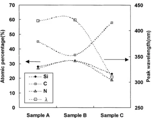
Fig. 5. The atomic percentage of Si–C–N films and the corresponding CL peak wavelength of samples A, B and C.
structure of the films can be manipulated through applica-tion of interlayer and selecapplica-tion of raw material sources.
The CL spectra of sample A, B and C are shown in Fig. 4. It indicates that the peak positions are at 419 nm (2.96 eV), 421 nm (2.94 eV) and 310 nm (4.00 eV), respectively. It implies that the sample C, which is C-rich and is deposited without additional Si source, has a higher energy gap. In other words, carbon atoms replace a part of nitrogen posi-tions in the crystals. Fig. 5 represents the correlation between
film compositions and CL peak wavelength. The higher Si or N contents will result in the higher CL peak wavelengths, or the lower band gaps. The energy gaps for samples A, B and C are below gaps for Si3N4 crystals (4.7–4.9 eV) and close to the predicted gaps for hypothetical-C3N4crystals (indirect band gap= 3.2 eV and direct band gap = 4.0 eV) [11,12].
4. Conclusions
A property tunable process was successfully designed to change the energy gaps of the Si–C–N films through a simple process to alter the crystal structure and film compo-sitions. The key point of this new process is in engineering proper interlayer material and/or selecting raw material sources to tune the film properties. The Co interlayer has successfully demonstrated the possibility. The XPS results indicate the existence of multiple binding structures and the mixture of sp2and sp3bonding of C and N in the films, but no detectable Co bonding and Si–C bonding in the films. Therefore, Co interlayer seems to be an effective catalyst for Si–C–N nucleation. Effect of Co on Si–C–N nucleation will be an interesting topic.
Acknowledgements
This work was supported by the National Science Council (contract No. NSC89-2216-E009-020) and the Ministry of Education of Taiwan (contract No. 89E-FA06-1-4).
References
[1] L.C. Chen, C.T. Wu, J.J. Wu, K.H. Chen, Inter. J. Mod. Phys. B 14 (2000) 333.
[2] A. Badizian, T. Badizan, R. Roy, W. Drawl, Thin Solid Films 354 (1999) 148.
[3] A. Badizian, T. Badizan, W. Drawl, R. Roy, Dia. Relat. Mater. 7 (1998) 1519.
[4] L.C. Chen, K.H. Chen, S.L. Wei, P.D. Kichambare, J.J. Wu, T.R. Lu, C.T. Kuo, Thin Solid Films 355–356 (1999) 112.
[5] K.H. Chen, J.J. Wu, L.C. Chen, C.Y. Wen, P.D. Kichambare, F.G. Tarntair, P.F. Kuo, S.W. Chang, Y.F. Chen, Dia. Relat. Mater. 9 (2000) 1249.
[6] P. Piedigrosso, Z. Konya, J.F. Colomer, A. Fonseca, G.V. Tendeloo, J.B. Nagy, Phys. Chem. Chem. Phys. 2 (2000) 163.
[7] J.S.M. Zadeh, K.J. Smith, J. Catal. 176 (1998) 115.
[8] T.H. Huang, C.T. Kuo, T.S. Lin, Surf. Coat. Technol. 56 (1993) 105. [9] A. Alberti, F. La Via, V. Raineri, E. Rimini, J. Appl. Phys. 86 (1999)
3089.
[10] H. Zhang, J. Poole, R. Eller, M. Keefe, J. Vac. Sci. Technol. A 17 (1999) 1904.
[11] A.Y. Liu, M.L. Cohen, Phys. Rev. B 41 (1990) 10727. [12] R.D. Carson, S.E. Schnatterly, Phys. Rev. B 33 (1986) 2432.