light-emitting device (OLED) current ratio can be achieved, without increasing the a-Si:H TFT size, by using a cascade struc-ture of storage capacitors. Moreover, the proposed circuit can compensate for the variations of TFT threshold voltage. Sim-ulation results, based on a-Si:H TFT and OLED experimental data, showed that a data-to-OLED current ratio larger than 10 and a fast pixel programming time can be accomplished with the proposed circuit.
Index Terms—Active-matrix, active-matrix organic light-emit-ting displays (AM-OLEDs), current driving, current scaling, light-emitting diode (LED), organic light-emitting displays (OLED), polymer light-emitting device (PLED), thin-film transistor.
I. INTRODUCTION
S
INCE the first observations of the light emission in small molecules based organic light-emitting diodes (OLEDs) [1], there have been increasing interest in their applications to a large area flat panel displays due to their adequate opto-electric properties, versatility of colors, large viewing angle and potentially a low fabrication cost [2]–[4]. At the same time, for a number of years hydrogenated amorphous silicon thin-film transistor (a-Si:H TFT) and a low-temperature polysilicon (LTPS) TFT active-matrix (AM) array have been developed for liquid-crystal displays (LCDs). Recently it was also demonstrated that a combination of the OLEDs with the TFT active-matrix arrays can be used for a high resolution ac-tive-matrix OLEDs [5]–[10]. Since the AM-OLED luminance is directly proportional to the driving current passing through it, the pixel electrode circuits must deliver continuous current to OLED during the whole frame period [11].To modulate the OLED current, two approaches have been often used. In the first approach, a voltage signal is used to di-Manuscript received November 1, 2004; revised March 4, 2005. The review of this paper was arranged by Editor J. Hynecek.
Y.-C. Lin is with the Solid-State Electronics Laboratory, Department of Elec-trical Engineering and Computer Science, University of Michigan, Ann Arbor, MI 48109 USA. He is also with the Optical Storage and Display Laboratory, In-stitute of Electro-optical Engineering, National Chiao-Tung University, Hsinchu 300, Taiwan, R.O.C. (e-mail: [email protected]).
H.-P. D. Shieh is with the Display Institute, National Chiao-Tung University, Hsinchu 300, Taiwan, R.O.C. (e-mail: [email protected]).
J. Kanicki is with the Solid-State Electronics Laboratory, Department of Elec-trical Engineering and Computer Science, University of Michigan, Ann Arbor, MI 48109 USA (e-mail: [email protected]).
Digital Object Identifier 10.1109/TED.2005.848119
to the device aging can result in nonuniform luminance over the display area [6], [7], [10]. Current driving schemes with four-TFT pixel electrode circuits have been proposed as other approach to drive AM-OLED, whereby the current signal pro-vided by external driver modulates directly the pixel electrode circuits [9], [10]. The four-TFT circuits can not only provide a continuous excitation to OLED, but at the same time it can also compensate for the TFT threshold voltage variation.
Although the current driving scheme improves the display lu-minance uniformity, a large timing delay can be observed at a low data current that is due to combination of a high OLED efficiency and charging of a large interconnect parasitic capaci-tances. For example, a current of 70 nA is sufficient to achieve luminance of 100 when an OLED with efficiency of 20 cd/A or higher is used. However, for such small current an in-terconnect parasitic capacitance of about 10 pF needs more than 150 s to build up a sufficient voltage level. This charging time is much larger than 30 s, that is needed for a display with VGA resolution operated at 60 Hz. To reduce the programming time delay, the pixel electrode circuits based on an adjustable TFTs geometric ratio with the current scaling function have been proposed [12], [13]. One example of such circuit is current mirror type pixel electrode circuit, Fig. 1(a). In this circuit a high data-to-OLED-current ratio can only be achieved for a large geometric ratio of T4 to T3. This can sig-nificantly limit the pixel electrode aperture ratio. A possible so-lution to this problem is top emission OLED structure in which a nearly entire pixel area could be used as light-emitting region [14]. In general, the pixel aperture ratio should not be influenced by the size of TFT and the complexity of pixel electrode circuit. This is especially true for high resolution displays. For example, the pixel size of display with resolution higher than 200 ppi is around m [15], so that the T4/T3 ratio is limited to 2.5/1 when T3 width is of 50 m. Consequently, the current scaling ratio of current mirror type pixel electrode circuit cannot be effectively used when the display resolution increases.
In this paper, we present an improved current driver pixel circuit based on a-Si:H TFT technology with a novel current scaling function. A cascade structure of storage capacitors is proposed here to achieve a high data-to-OLED-current ratio without increasing TFTs size in comparison to a conventional current mirror pixel circuit, shown in Fig. 1(a). The proposed pixel electrode circuit can also compensate for a-Si:H TFT threshold voltage variation so that uniform display luminance 0018-9383/$20.00 © 2005 IEEE
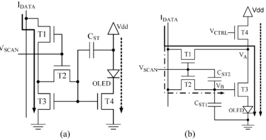
Fig. 1. Schematic diagrams of current driven pixel circuits with (a) conventional current mirror and (b) cascade structure of storage capacitors.
is expected. First, we describe the structure and discuss the oper-ation principles of pixel electrode circuit. The parameters used for circuit simulation are discussed in Section III. The simula-tion results and circuit performance are discussed in Secsimula-tion IV, with conclusion presented in Section V.
II. PROPOSEDPIXELELECTRODECIRCUIT
The proposed current driven pixel electrode circuit consists of three switching TFTs (T1, T2, T4), one driving TFT (T3) and two storage capacitors ( , ) connected between a scan line and ground with a cascade structure, as shown in Fig. 1(b). The operation of the circuit is controlled by four external ter-minals: , , , , and ground. The signals of , , and are supplied by external drivers while the cathode of OLED is grounded. It should be noticed that to simplify the circuit analysis, one node of connected to the ground is adopted. In practice, the ground electrode of needs additional routing and contact via to connect with the OLED grounded cathode. Therefore the can be con-nected to the line instead of the ground in order to reduce the layout area. The electrode is connected to the external power supply to provide a constant voltage signal to the pro-posed pixel circuit. The operation of this pixel electrode circuit can be described as follows.
During theON-state, the scan line signal turns on the switching transistors T1 and T2. During this time, a data current signal passes through T1 and T3 to OLED, shown as the solid line in Fig. 1(b), and sets the voltage at the T3 drain electrode (nodes A). At the same time the voltage at the T3 gate electrode (node B) is set by passing through T2 (dash line). The control signal turns T4 off to ensure that no current flows through T4. Consequently, in an ideal case the OLED current inON-state, , should be equivalent to . Since the T3 drain and gate electrodes are at the same potential, T3 will operate in the deep saturation region, e.g.,
(threshold voltage) and the and voltages at both nodes are determined automatically according to (1):
(1)
where , , and are field-effect mobility, gate oxide capacitance, width and length of TFT(T3), respectively. If T3 threshold voltage changes and if this change is not higher than amplitude, the T3 gate voltage, , will be ad-justed accordingly to ensure the identical in theON-state. Therefore, is always adjusted to keep at about the same value regardless of a-Si:H TFT threshold voltage. The will be stored in both and and the voltage
across is .
When the pixel changes from the ON- to the OFF-state, turns off T1 and T2, and simultaneously turns on T4. Because is connected between the scan line and the node B to form a cascade structure with ,
change from high to ground state will reduce
to due to the feed-through effect of the capacitors. can be derived from the charge conservation theory, and is given by (2), in which and are an
amplitude of and the
gate-to-source/drain overlap capacitance of T2, respectively (2) A reduced T3 gate voltage, , will be hold in and and it will continuously turn on T3 during this time pe-riod. Since the overdrive voltage of T4
is lower than , the T4 is working in saturation region. In order to ensure that the is similar to and the T3 is operating in the deep saturation region, the width of T4 should be large enough to reduce the turn-on resistance of T4. A cur-rent smaller than , shown as the dash line in Fig. 1(b), will be generated by and will pass through T4 and T3 to OLED. Consequently, the OLED current in OFF-state,
, will be smaller than .
Since the T3 gate voltage decreases from
to , the OLED driving current is scale-down from ON- to OFF-state by the storage capacitor cas-cade structure. The quantity of voltage drop, shown as in (2), will increase with increasing , and values and will lead to a smaller . In other words,
the scale-down ratio, ,
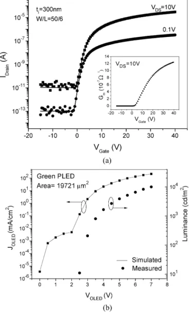
Fig. 2. (a) Transfer characteristics of a-Si:H TFT. The transconductance versus gate voltage is shown in insert. (b) An example of measured PLED current density and brightness variation with supplied voltages.
the small geometric size is adequate for switching TFT T2, the small which is parallelly connected to the can be regarded as a portion of . Therefore it is expected that a larger will result in larger . Consequently, when a very large data current is used to charge the pixel electrode and to shorten the pixel programming time, at the same time a smaller driving current can be achieved for lower gray scales.
III. PARAMETEREXTRACTION ANDPIXELELECTRODE CIRCUITDESIGN
Synopsis H-SPICE simulation tool with the Rensselaer Poly-technic Institute (RPI) Troy, NY, a-Si:H TFT model [16], [17] was used to evaluate the proposed pixel electrode circuit. The a-Si:H TFT parameters developed within our group were used in this simulation [18], [19]. The transfer characteristics (
, drain current versus gate-to-source voltage) of a-Si:H TFT are shown in Fig. 2(a) and in the insert its transconductance is given. To simulate the behavior of OLED the conventional
semiconductor diode model, with the parameters extracted for organic polymer light-emitting device (PLED) fabricated in our laboratory, was used. The opto-electrical properties of PLED are shown in Fig. 2(b) and were described elsewhere [20]. In the pixel design, a with the fixed size of 2.5 pF was used and size was varied from 210 to 625 fF to achieve different ratios. Since T2 works as a switch in this circuit, its size can be smaller in comparison with other TFTs. Based on our own experience we believe that a high-performance a-Si:H TFT with higher than 1.5 cm V/s is essential for future a-Si:H TFT pixel electrode circuit. The a-Si:H TFT with lower will need a higher driving voltage and larger geometric size to achieve an adequate OLED driving current level. Then, in-creased display power consumption and reduced pixel aperture ratio, when light is emitted through the substrate, are expected. In addition, it is expected that a higher performance TFT will have better electrical stability over the time. The a-Si:H TFTs and OLED parameters used for this pixel electrode circuit sim-ulation are given in Table I.
IV. SIMULATIONRESULTS ANDDISCUSSION
A. Current-Scaling Ratio
The proposed current-scaling pixel electrode circuit was evaluated using H-SPICE and an example of the waveforms is shown in Fig. 3. In this specific case, inON-state, the voltages at node A and B are set to appropriate levels to allow of 4 A to pass through T3. It should be noticed that in ideal
Fig. 3. Example of pixel operation waveforms simulated by H-SPICE for V = 35 V.
case the voltages at A and B nodes are identical. However, in practice, there will be a difference between A and B voltages because passing through T1 causes a voltage drop between drain and source electrodes of T1. InOFF-state, in this special case the T3 gate voltage decreases from 13.3
to 9.2 V and changes from 12.3 to 28.1 V. higher than keeps T3 operating in deep saturation region and the drop of results in reduction of from
4 to 1.4 A . This figure
clearly shows that is different from and the
is obtained.
Since is larger than by
a factor of , the average OLED current for the pixel electrode circuit must be properly defined
(3) where and denote the select and deselect periods during the frame time, respectively.
Since the , (3) can be
written as
(4)
Fig. 4. Variation of the scale-down ratio versus (a) data current and (b) ratio of storage capacitances.
From this equation an accurate can be calculated for
various combinations of and to satisfy
the display requirements for different gray scales. As it will be shown below to be able to display low gray scales, not only a
low but also a high are needed, at the
same time, to control both a low display luminance and a fast programming time. Combination of a low and a large can be used to satisfy such display requirement. For higher gray scales, a high is not needed since a high can be achieved. Therefore, a combination
of a large and a low is appropriate to
display high gray scales. Since the scaledown ratio
, will affect the performance of the proposed pixel electrode circuit, it is important to evaluate its evolution with
the and . The variation of
as a function of is shown in Fig. 4(a). From this figure we can conclude that when , decreases from 210 to 1.5 as increases from 0.1 to 10 A. In this specific case since at a high gray scale is larger than that at a low gray scale, it is expected that
. The simulation results showed that when is fixed, increases when increases from 210 to 625 fF, corresponding to an increase of from 1/12 to 1/4. Fig. 4(b) also demonstrates that when a smaller is used, a higher can be achieved with the constant
.
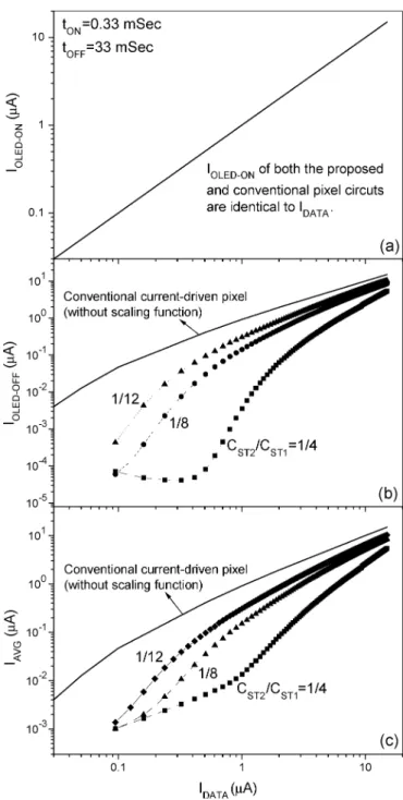
The current-scaling function is performed so that the large programming current can be reduced to an appropriate value when the pixel operates from the ON- to the OFF-state. In ON-state, the are identical in not only the conventional but also the proposed pixel electrode cir-cuits because the external driver directly controls the current, Fig. 5(a). When pixels work in OFF-state, the proposed pixel circuit reveals superior current-scaling ability in comparison with the conventional current-driven pixel electrode circuit [9], [10] which just ideally keeps the equiva-lent to [Fig. 5(b)]. It should be noticed that the versus of the conventional pixel circuit changes from linear to curved behavior due to the charge injection phenomenon. This charge injection can occur when the gate voltage is removed, and when the charge carriers in the T2 channel are released and redistributed into the drain and source electrodes. The carrier redistribution will alter the voltages at both nodes. Therefore, the charge injection from
T2 causes the slightly deviate from .
From Fig. 5(b), it is obvious that the large results in significant decrease of the . Moreover, since the OFF-state period is much longer than ON-state, the small inOFF-state can further reduce the even if the is large. Using (3), the plots of versus
in one frame period
with ratios as a parameter are shown in Fig. 5(c). For example, the proposed pixel electrode circuit can generate ranging from 1 nA to 5 A with ranging from 0.1 to 10 A. By contrast, the of conventional pixel electrode circuit is almost equal to . In other words, a very small can only be achieved by the having a similar magnitude. From these figures, it is evident that larger than can be used to program the proposed pixel circuit inON-state without increasing the a-Si:H TFTs geometric size. Hence, using an additional to form a cascade capacitors structure, a large can be achieved and a high can be used to accelerate the pixel circuit programming in ON-state.
Fig. 5. Variation of theI ,I andI during one frame period versusI (= I ) at various C =C ratio.
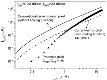
To demonstrate the proposed pixel electrode circuit out-standing current scaling function in comparison with both the conventional current-driven and current-mirror pixels, one simulated as a function of for each pixel electrode circuit is shown in Fig. 6. Although the current-mirror pixel is able to scale down , the scale-down ratio is constant in the whole range of . In current-mirror pixel, a large for high gray scales will result in a high power consumption due to the fixed scale-down ratio. In addition, to achieve the current scaling function, a larger driving TFT T4 needed in the current-mirror pixel will substantially reduce the pixel electrode aperture ratio. From Fig. 6, we can conclude that with the ranging from 0.1 to 10 A, our proposed pixel circuit can achieve ranging from 1 nA to 5 A,
Fig. 6. Comparison ofI as a function ofI among conventional current-driven, current-mirror, and proposed pixels.
which represents a much wider range in comparison with the conventional current-driven pixel (0.05 to 10 A) and the current-mirror pixel (0.01 to 2.5 A). Therefore, the proposed pixel circuit can yield not only a high and a high for the low gray scales, but also reasonable for a high gray scale to avoid large display power consumption.
B. Influence of Threshold-Voltage Variation
To investigate the influence of variations of T3 and T4 on pixel circuit performance, various threshold voltage deviations after stress (initial)), based on the exper-imental results reported in [19], have been used in pixel circuit simulation. Since the is not affected by and the is related to through (4), the variation of with the TFT threshold voltage is used to estimate the influence of on pixel circuit operation.
For , the variation of the ,
de-fined by (5), with can be calculated
(5) The variation of as a function of is shown in Fig. 7(a). Following the increase of ,
gradually increases from around 1 to 6% when is
higher than 1.0 A. The up to 6% at of
4 V can be reached. This is due to turn-on resistance of T4 and channel length modulation of T3. In ideal case,
of T3 operating in saturation mode is independent of drain voltage . However, in practice the TFTs are impacted by the channel length modulation and the drain voltage variation can only slightly affect . Since the turn-on resistance of T4 changes with the increase, the T3 can suffer a serious drain voltage offset between ON- and OFF-state so that the can be changed. In other words, an increase of with a high T4 turn-on resistance can lead to a decrease of and consequently can result in a large , Fig. 7(b). In order to suppress the effect of T4 , a higher or T4 with a larger width can be used
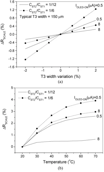
Fig. 7. (a) Variation of 1I as function of TFT threshold voltage shift. (b) 1I versus OLED current during display operationOFF-state for differentC =C and1V = 4V. The data for 1V = 1 V is shown in insert.
to reduce the turn-on resistance of T4. However, an additional voltage signal can increase the complexity of peripheral drivers and a larger T4 can slightly decrease the pixel aperture ratio for bottom light-emission OLED structure.
Substantial increase of when is
lower than 100 nA is due to the influence of charge injection of switching T2 on . Since a small will result from a low driving current at low gray scales, the charge carrier released from T2, when T2 is turn-off, can reduce the . Therefore, can be modified by not only a voltage drop induced by cascade structure of and but also by a charge injection from T2. In addition, the shift of all TFTs can lead to a higher sensitivity of to the charge injection from T2. Therefore, large storage capac-itor is needed to eliminate the effect of T2 charge injection. As shown in Fig. 7(b), when large is used, a signifi-cant reduction of at low gray scales is observed
OLED current in -state can be given as
(6)
where ,
. Equation (6) can be rewritten as
(7) It should be noted that in the second and third terms of (7) is temperature and mismatch sensitive, hence the will be influenced by temperature, resulting in variation of . Fig. 8(a) shows the variation of with T3 size
mismatch. The changes by 1.2% as the T3 width varies from 147 to 153 m, corresponding to 2% deviation. Also, according to (7), a higher offset voltage value, as-sociated with a large ratio, will introduce greater scale-down ratio deviation , Fig. 8(a). Finally, the in a high gray scale is not as large as that in a low gray scale because a high driving current can reduce its sensi-tivity to the geometric size mismatch.
Since the field-effect mobility can be affected by device temperature, it is expected that in (6) will also have tempera-ture dependence [21], [22]. The temperatempera-ture increasing from 20 to 70 C will result in a higher field-effect mobility thus giving a rise in [Fig. 8(b)]. Also, a higher due to a larger ratio can cause an increase of not only in a high gray scale A but also in a low gray scale A regions. It should be men-tioned that as the driving current increases, becomes smaller as a result of low temperature sensitivity achieved by a
larger .
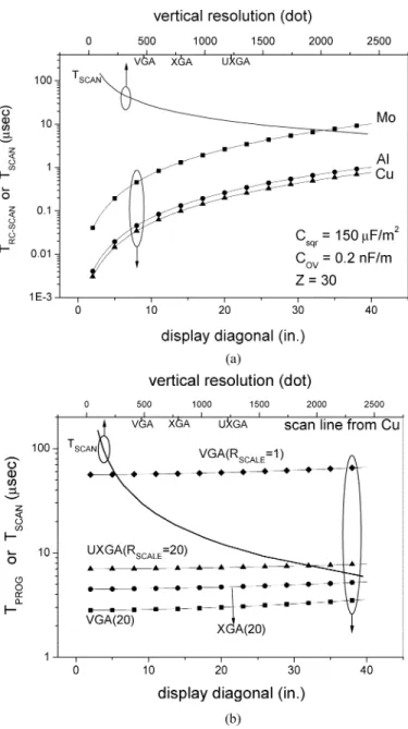
D. Scan Line Delay in High-Resolution Display
The key factor to realize a large size and a high resolution dis-play is to overcome the long resistance-capacitance (RC) time constant of the bus lines of which the resistance and capacitance are proportional to the size and the resolution of display panel. A large RC time constant can cause cross-talk and flicker effects due to the insufficient pixel charging across the large display area. Since the bus line resistance is due to intrinsic resistance
Fig. 8. (a) Variation of R as a function of T3 width variation. (b) Influence of operation temperature uponR .
of bus lines materials and capacitance is associated with overlap capacitance of intersections and TFTs, the RC time constant of scan line can approximately estimated by the fol-lowing equation:
(8) where , , , , , and are display width, hori-zontal resolution, capacitance per meter square, sheet resistance, pixel pitch to bus line width ratio and TFT gate-to-drain/source overlap capacitance. According to (8), it is expected that a larger panel size and a higher display resolution will cause a longer which can affect the data programming precision.
Fig. 9. (a) Dependence of scan line RC time constant(T ) on display diagonal and the relationship between scan pulsewidth(T ) and resolution. (b) Data programming time(T ) as a function of panel resolution with a scan line made from Cu.
the as a function of display diagonal was calcu-lated for UXGA resolution and for different metallurgy, e.g.,
copper , aluminum (0.1 ) and
molyb-denum (1.0 ), Fig. 9(a). The scan pulsewidth shown as the solid line in Fig. 9(a) is also evaluated for 60-Hz frame rate and for different vertical resolutions. In general, the should be ten times larger than to prevent the data programming error. Therefore, based on this simple calculation a high-resistance material such as molybdenum will limit the display size to about 12 in with UXGA resolution. A low-resis-tance material such as aluminum or copper is capable to reduce in large size display up to 35 in or higher to accept-able value.
For AM-OLED, not only the but also the data programming time is important. The is directly related to the data line capacitance , storage capacitance
and the programming current and can be approxi-mated by the following equation:
(9)
where .
Since the is much smaller than , it can be neglected to simplify the calculation. In (9), denotes the voltage at generated by the , and is the vertical resolution which can be obtained from and aspect ratio of display. The constants , , and depend on the refractive index and the emission spectrum of the OLED material [23]. Besides, L is the OLED luminance and is device quantum efficiency [23]. It should be noted that the in (9) is independent of the display size, and is increased when the pixel area is increased to compensate for large resulting from the increase of display size. In order to compare the proposed pixel electrode circuit with the conventional pixel circuit and to evaluate its performance, is defined as to describe the total time requirement for accurate data programming. Fig. 9(b) shows of proposed pixel as a function of display size for V, ,
V , lm/W, , ,
and , along with the
of conventional pixel for . Without current scaling
function , a VGA display requires of
s to charge up the conventional pixel electrode circuit which is two times higher than a specific of display with VGA resolution. Therefore conventional pixel circuit is not applicable for a large size and a high resolution display device. By contrast, the proposed pixel circuit with the current scaling function can reduce the significantly when a large is used. Furthermore, as display resolution increases, the for UXGA resolution (1600 1200) is of s which is lower than a specific of 10 s even for display diagonal of 40 in. In summary, the proposed pixel electrode circuit with cascade storage capacitance has built-in current scaling capability that could allow to achieve a high resolution and a large size current-driven AM-OLED.
V. CONCLUSION
We proposed a pixel electrode circuit based on a-Si:H TFT technology and current driving scheme for speeding up the data programming time. We have shown that this circuit can achieve a high current scale-down ratio by a cascade structure of storage capacitors instead of increasing the size of TFT. In the proposed circuit, the ON-state data current of a factor of 10 larger than OLED current inOFF-state can be achieved. In contrast to the conventional current-driven and the current-mirror pixel elec-trode circuits, our pixel circuit can achieve the widest range of for ranging from 0.1 to 10 A, hence both the current scaling function and the reasonable power consumption can be easily accomplished without substantially sacrificing the pixel aperture ratio. Furthermore, the threshold voltage variation of all TFT can also be compensated by the proposed circuit. The effects of device geometric size mismatch and temperature in-crease on pixel electrode circuit were analyzed, and it has been
[2] C. W. Tang, “Organic electroluminescent materials and devices,” Inform.
Displ., vol. 12, no. 10, pp. 16–19, 1996.
[3] J. H. Burroughes, D. D. C. Bradley, A. R. Brown, R. N. Marks, K. Mackay, R. H. Friend, P. L. Burns, and A. B. Holmes, “Light-emitting diodes based on conjugated polymers,” Nature, vol. 347, pp. 539–541, 1990.
[4] A. J. Heeger and J. Long Jr., “Optoelectronic devices fabricated from semiconducting polymers,” Opt. Photon. News, vol. 7, no. 8, pp. 23–30, 1996.
[5] C. C. Wu, S. Theiss, M. H. Lu, J. C. Sturm, and S. Wagner, “Integration of organic LEDs and amorphous Si TFTs onto unbreakable metal foil substrates,” in IEDM Tech. Dig., 1996, pp. 957–959.
[6] M. Stewart, R. S. Howell, L. Pires, M. K. Hatalis, W. Howard, and O. Prache, “Polysilicon VGA active matrix OLED displays—technology and performance,” in IEDM Tech. Dig., 1998, pp. 871–874.
[7] T. Shimoda, H. Ohsima, S. Miyashita, M. Kimura, T. Ozawa, I. Yu-dasaka, S. Kanbe, H. Kobayashi, R. H. Friend, J. H. Burroughes, and C. R. Towns, “High resolution light emitting polymer display driven by low temperature polysilicon thin film transistor with integrated driver,” in Proc. Asia Display Conf., 1998, p. 271.
[8] R. M. A. Dawson, Z. Shen, D. A. Furst, S. Connor, J. Hsu, M. G. Kane, R. G. Stewart, A. Ipri, C. N. King, P. J. Green, R. T. Flegal, S. Pearson, W. A. Barrow, E. Dickley, K. Ping, C. W. Tang, S. Van Slyke, F. Chen, J. Shi, J. C. Sturm, and M. H. Lu, “Design of an improved pixel for a polysilicon active matrix organic LED display,” in Proc. SID, 1998, pp. 11–14.
[9] Y. He, R. Hattori, and J. Kanicki, “Current-source a-Si:H thin-film tran-sistor circuit for active-matrix organic light-emitting displays,” IEEE
Electron Device Lett., vol. 21, no. 12, pp. 590–592, Dec. 2000.
[10] , “Improved A-Si:H TFT pixel electrode circuits for active-matrix organic light emitting displays,” IEEE Trans. Electron Devices, vol. 48, no. 7, pp. 1322–1325, Jul. 2001.
[11] M. K. Hatalis, M. Stewart, C. W. Tang, and J. Burtis, “Polysilicon TFT active matrix organic EL displays,” in Proc. SPIE, vol. 3057, 1997, pp. 277–286.
[12] A. Yumoto, M. Asano, H. Hasegawa, and M. Sekiya, “Pixel-driving methods for large-sized poly-Si AM-OLED displays,” in Proc. Int.
Dis-play Workshop, 2001, pp. 1395–1398.
[13] J. Lee, W. Nam, S. Jung, and M. Han, “A new current scaling pixel circuit for AMOLED,” IEEE Electron Device Lett., vol. 25, no. 5, pp. 280–282, May 2004.
[14] T. Sasaoka, M. Sekiya, A. Yumoto, J. Yamada, T. Hirano, Y. Iwase, T. Yamada, T. Ishibashi, T. Mori, M. Asano, S. Tamura, and T. Urabe, “A 13.0-inch AM-OLED display with top emitting structure and adaptive current mode programmed pixel circuit (TAC),” in Proc. SID, 2001, pp. 384–387.
[15] Y. Hosoya and S. L. Wright, “High resolution LCD technologies for the IBM T220/T221 monitor,” in Proc. SID, 2002, pp. 83–85.
[16] M. S. Shur, H. C. Slade, T. Ytterdal, L. Wang, Z. Xu, K. Aflatooni, Y. Byun, Y. Chen, M. Froggatt, A. Krishnan, P. Mei, H. Meiling, B.-H. Min, A. Nathan, S. Sherman, M. Stewart, and S. Theiss, “Modeling and scaling of a-Si:H and poly-Si thin film transistors,” in Proc. Mater. Res.
Soc. Symp., vol. 467, 1997, pp. 831–842.
[23] G. Gu and S. R. Forrest, “Design of flat-panel displays based on organic light-emitting devices,” IEEE J. Sel. Topics Quantum Electron., vol. 4, no. 1, pp. 83–99, Jan. 1998.
Yen-Chung Lin was born in Taiwan, R.O.C., on April 27, 1977. He received
the B.S. degree in electrical engineering from National Tsing-Hua University, Hsinchu, Taiwan, in 1999. He is currently pursuing the Ph.D. degree in electro-optical engineering, from the National Chiao-Tung University, Hsinchu.
His research interest is the circuit design for display applications and fabri-cation of thin-film transistors.
Han-Ping D. Shieh received the B.S. degree from National Taiwan University,
Taipei, Taiwan, R.O.C., in 1975 and the Ph.D. degree in electrical and computer engineering from Carnegie Mellon University, Pittsburgh, PA, in 1987.
He was a Research Staff Member with the IBM T. J. Watson Research Center, Yorktown Heights, NY. He then joined the Institute of Electro-Optical Engi-neering and Microelectronics and Information Research Center, National Chiao-Tung University, Hsinchu, Taiwan, as a Professor in 1992. He is also holding a joint appointment as a Research Fellow at the Center for Applied Sciences and Engineering, Academica Sinica, since 1999. His current research interests are in display technology, optical MEMS, nano-optical components, and optical data storage technologies. He has published more than 80 journal papers and has more 20 patents.
Dr. Shieh currently serves as the Director, Society for Information Display (SID), and has served as Program Chair, Committee Member, and has organized conferences in major data storage including ISOM, MORIS, Intermag, ODS, APDSC and display including SID, IDRC, ASID, FPD Expo, etc.
Jerzy Kanicki (M’99–A’99–SM’00) received the
D.Sc. degree from the Universit Libre de Bruxelles, Brussels, Belgium, in 1982.
He then joined the IBM Thomas J. Watson Research Center, Yorktown Heights, NY, as a Research Staff Member working on hydrogenated amorphous silicon devices for the photovoltaic and flat-panel display applications. In 1994, he moved from the IBM Research Division to the University of Michigan, Ann Arbor, as a Professor in the Department of Electrical Engineering and Computer Science (EECS). His research interests within the Electrical and Computer Engineering (ECE) Division of the EECS include organic and molecular electronics, TFTs and circuits, and flat-panel displays technology, including organic light-emitting devices.