This content has been downloaded from IOPscience. Please scroll down to see the full text.
Download details:
IP Address: 140.113.38.11
This content was downloaded on 25/04/2014 at 10:43
Please note that terms and conditions apply.
DC baseband and high-frequency characteristics of a silicon nanowire field effect transistor
circuit
View the table of contents for this issue, or go to the journal homepage for more 2009 Semicond. Sci. Technol. 24 045004
(http://iopscience.iop.org/0268-1242/24/4/045004)
Semicond. Sci. Technol. 24 (2009) 045004 (8pp) doi:10.1088/0268-1242/24/4/045004
DC baseband and high-frequency
characteristics of a silicon nanowire field
effect transistor circuit
Yiming Li
1and Chih-Hong Hwang
Department of Communication Engineering, National Chiao-Tung University, Hsinchu 300, Taiwan, Republic of China E-mail:[email protected] Received 25 November 2008 Published 27 February 2009 Online atstacks.iop.org/SST/24/045004 Abstract
Silicon-based nanowire field effect transistors (FETs) are potentially next-generation candidates for achieving high-performance targets of the International Roadmap for Semiconductors due to their superior reduction of the short-channel effects and excellent compatibility with planar complementary metal oxide semiconductor (CMOS) fabrication process. In this work, we for the first time numerically explore the dc baseband and high-frequency characteristics, and the design of the device aspect ratio (channel
length/channel thickness) for the silicon nanowire FET circuits by using a three-dimensional device/circuit-coupled mixed-mode simulation technique. With the experimentally validated simulation approach, the result shows the rather prolific dc baseband and high-frequency properties of silicon-based nanowire FET devices as active components. In design of silicon nanowire FETs, taking the nanowire’s radius and channel length as two crucial factors, the demands of the device aspect ratio on dc characteristics are found to be inversely proportional to the demands of the high-frequency characteristics. Therefore, to compromise both the dc and high-frequency characteristics, the design margin of the device aspect ratio restricted, in which the requirements of dc and high-frequency characteristics provide aspect ratio upper and lower bounds, respectively. Moreover, the design margin will be more tightened for a device with larger radius due to the weakened channel controllability. The extensive results and analyses are presented for the promising devices for the design of high-frequency analog applications.
(Some figures in this article are in colour only in the electronic version)
1. Introduction
High-frequency and wide-bandwidth requirement of complementary metal oxide semiconductor (CMOS) transistors has become a bottleneck for advanced electronic circuits and systems, such as wireless communication and digital multimedia. Accordingly, nanoscale CMOS devices with vertical channel structures, such as double-, triple- and surrounding-gate fin-type field effect transistors (FinFETs), are of great interest [1–27] because they inherently have good suppression of short-channel effects, high transconductance and ideal subthreshold swing (SS). The microwave
small-1 Author to whom any correspondence should be addressed.
signal characterization of a 50 nm gate FinFET measurement has predicted the maximum oscillation frequency of 250 GHz with an optimized fabrication process [22]. Among the nanoscale multiple-gate devices, the silicon-based nanowire FETs have the ultimate gate structures and become potential candidates for next-generation high-speed and high-power electronic devices [12–27]. Besides the perfect channel controllability resulting from the nature of the gate-all-around channel [19–21], the nanowire FETs may tolerate having a thicker silicon fin, compared with double- and triple-gate FinFETs according to the manufacturability point of view [20, 21]. Various studies were performed on the dc characteristics and their manufacturing techniques using
Semicond. Sci. Technol. 24 (2009) 045004 Y Li and C-H Hwang silicon-based nanowire FETs in the device level [16,22–27].
However, for the high-frequency characteristics of silicon nanowire FETs, the analog circuit and its design consideration have not been discussed yet.
In this work, we numerically provide an insight into the dc baseband and high-frequency response of the nanoscale silicon nanowire FET circuit. To provide a more physical insight into the device and pursue high simulation accuracy, we develop a device/circuit coupled mixed-mode simulation technique [28–32] to explore the nanowire transistor circuit behavior due to the lack of a well-established equivalent circuit model of silicon nanowire FETs. The three-dimensional (3D) device transport equations with quantum corrections by the density gradient method [33–36] are directly coupled with circuit conservation equations and simultaneously solved on a parallel computing system [37–39]. We notice that the 3D simulation has been advanced and calibrated with experimentally measured results for both the planar and nanowire devices in our recent investigations [1–3,12,19–21,
31,39,40]. The extensive results and analyses presented for the promising devices for high-frequency analog application show the promising high-frequency characteristics of the nanowire FET circuit. Considering the radius (R) and gate length (Lg) of the silicon nanowire FET, in the design of
silicon nanowire FETs, the aspect ratio (it is equal to the channel length divided by the channel thickness, where the channel thickness Tsi = 2R) is considered as a main factor
in determining both dc and high-frequency characteristics; however, the demands of the aspect ratio on dc characteristics are found to be inversely proportional to the demands of the high-frequency characteristics according to the results of this study. Thus, to properly compromise the dc and high-frequency characteristics, the design margin of the aspect ratio is more tightened than that found in the results reported in [20, 21]. The requirements of dc and high-frequency characteristics provide the upper and lower bounds of the device aspect ratio, respectively. For example, to obtain a device with a subthreshold swing smaller than 75 mV/dec and a gain–bandwidth product larger than 3.5 × 10¹², the
aspect ratio should be controlled between 2 and 3.5. Moreover, the design margin is more tightened for a device with larger radius. This theoretical study provides an insight into high-frequency characteristics of the silicon nanowire FET circuit and shows the design consideration of the nanowire FET. The extensive results and analyses of this study are presented for the promising devices for high-frequency analog applications. This article is organized as follows. In section 2, we state the investigated device structure and circuit configuration including a brief of simulation methodology. In section3, the results of dc baseband and high-frequency characteristics of the studied devices and circuits are compared and discussed. Finally, we draw conclusions and suggest future work.
2. The nanowire FET circuit and simulation
methodology
To study the device geometry dependence on the dc and high-frequency characteristics of the silicon nanowire FET with
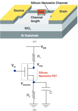
Source Source SiO SiO22 Si SiSubstrateSubstrate Drain Drain Gate Gate
Silicon Nanowire Channel
Silicon Nanowire Channel
Channel Channel length length (a) (b) VDD Vgate Silicon Nanowire FET Vsource Vdrain C R2 R1 Vin Vout
Figure 1. (a) Plot of studied silicon nanowire field effect transistors,
where the 100% surrounding-gate structure is assumed. (b) The circuit topology used in the 3D mixed-mode simulation.
100% gate coverage, as shown in figure1(a), the simulated nanowire FETs with different channel radii, i.e. 4 and 6 nm, corresponding to different gate lengths, i.e. 16, 32 and 45 nm, respectively, are considered. We note that the aspect ratio of silicon nanowire transistors could be larger than 0.5 or 1 due to different device specification [20,21,25]. Therefore, according to the specified target of dc baseband characteristics, the channel thickness is selected to keep the device aspect ratio near 1 for maintaining an acceptable dc characteristics. The channel doping concentration of the designed device is 2.3× 1017 cm−3 and the oxide thickness is 1.2 nm. Mid-gap gate material, TiN, is used in the device. Outside the channel, the level of source/drain doping is 3× 1020 cm−3. Three-dimensional drift–diffusion equations coupled with density-gradient quantum correction [33–36] are numerically solved to obtain the characteristics of the device [19–21] in the established parallel computing system [37–39]. A carefully calibrated density-gradient model [41,42] has attracted more and more attention, and successfully demonstrates its validity for efficient modeling of the quantum mechanical effects in a device simulation program using first-order quantum corrections [33–36]. This simulation quantitatively predicts the main tendency of electrical and physical properties for the examined device structures. Full quantum mechanical methodologies definitely will input more accurate estimation on the characteristics, but it is believed that our simulation will not be significantly altered. The density-gradient modeling approach is computationally effective for incorporating the quantum mechanical effect in a multidimensional nanodevice 2
simulation. The developed device simulation prototype has been calibrated and successfully validated in analyzing the effect of grain boundary on surrounding-gate polysilicon thin film transistors [39] and discrete impurity effect on a nanoscale MOSFET [2,39,40]. We also have studied the geometry effect in nanowire transistors [19,20] in our recent work. For the simulated silicon nanowire device in this study, the physical model of the device has been calibrated with the measurement results of 5 nm gate nanowire FETs [20,21]. In exploring the dc baseband and high-frequency characteristics of the silicon nanowire FET circuit, a common-source amplifier circuit is implemented as the tested circuit, as shown in figure1(b). A small signal input with 0.6 V offset voltage is used to explore the high-frequency characteristics of the silicon nanowire FET circuit. The 3D device transport equations with quantum corrections by the density gradient method [33–36] are directly coupled with circuit equations and simultaneously solved [28–32] to provide the best accuracy.
3. Results and discussion
It has been well known that the gate length and the radius of the silicon nanowire FET are the main factors in determining the characteristics of a nanowire transistor. In this section, we first discuss the geometry effect of silicon nanowire FETs on their dc characteristics. Then, we investigate the high-frequency response and design of the silicon nanowire FET circuit.
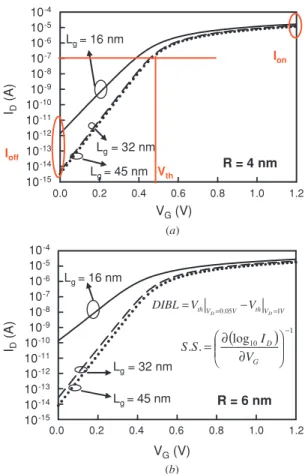
Figures2(a) and (b) show the ID–VG(drain current versus
gate voltage) characteristics for the studied nanowire FETs with 4 and 6 nm radius, respectively, where the definitions of the threshold voltage (Vth), on-state current (Ion),
off-state current (Ioff), drain-induced barrier lowering (DIBL)
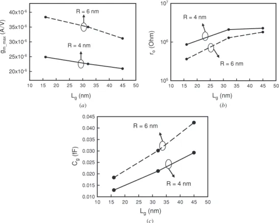
and subthreshold swing (SS) are illustrated and defined in the insets. In this study, the constraints of DIBL < 50 mV and SS < 75 mV/dec are used for the selection of a device with acceptable dc characteristics. We note that the selection criteria defined in this study provide an example of a device with a small acceptable short-channel effect. The selection criteria can be defined by designer’s purpose in different applications. The calculated dc characteristics are summarized in table 1. Due to superior channel controllability of nanowire devices with smaller radius, the 4 nm radius nanowire transistor exhibits a satisfied short-channel effect and a smoother threshold voltage roll-off than the 6 nm radius nanowire transistor. Figures 3(a)–(c) show the maximum transconductance (gm max), the output resistance (ro) and
the gate capacitance (Cg) of the studied silicon nanowire
devices, respectively. The device with a smaller radius shows a smaller gm max, a larger ro and a smaller Cg, which
agree with the dependence of the derived characteristics on device geometry, where gm maxis quantitatively proportional to
(VGS − Vth)RLg−1, ro is proportional to LgR−1(VGS− Vth)−2
[43] and Cg is proportional to Lg[ln(1 + toxR−1)]−1[27]. For
the design of nanoscale nanowire FETs, in order to have better controllability of the short-channel effect, the aspect ratio should be carefully designed with respect to specified device characteristics. Figure 4 shows the subthreshold swing as a function of the aspect ratio, where the circles
VG (V) 0.0 0.2 0.4 0.6 0.8 1.0 1.2 10-15 10-14 10-13 10-12 10-11 10-10 10-9 10-8 10-7 10-6 10-5 10-4 Lg= 32 nm Lg= 16 nm Lg= 45 nm ID (A ) VG(V) R = 4 nm Ion Ioff Vth VG (V) 0.0 0.2 0.4 0.6 0.8 1.0 1.2 10-15 10-14 10-13 10-12 10-11 10-10 10-9 10-8 10-7 10-6 10-5 10-4 Lg= 32 nm Lg= 16 nm Lg= 45 nm ID (A ) VG(V) R = 6 nm
(
)
1 10 log . . − ∂ ∂ = G D V I S S V V th V V th D V D V DIBL= =0.05 − =1 (a) (b)Figure 2. The ID–VGcharacteristics for the studied device with (a) 4 and (b) 6 nm radius, where the insets are the definitions of the on-state current (Ion), off-state current (Ioff), threshold voltage (Vth), drain-induced barrier lowering (DIBL) and subthreshold swing (SS).
Table 1. The summarized dc characteristics of the silicon nanowire
FET with 100% surrounding gate. In this study, the constraints of DIBL < 50 mV/V and SS < 75 mV/dec are used for the selection of a device with acceptable dc characteristics. The channel doping concentration of the designed device is 2.3× 1017cm−3, the gate work function is 4.6 eV and the oxide thickness is 1.2 nm. Outside the channel, the level of source/drain doping is 3× 1020cm−3.
R (nm) Lg(nm) Vth(V) Ion(A) Ioff(A)
4 16 0.383 1.65× 10⁻⁵ 1.36× 10⁻¹² 4 32 0.456 1.30× 10⁻⁵ 4.81× 10⁻¹⁵ 4 45 0.464 1.16× 10⁻⁵ 3.29× 10⁻¹⁵ 6 16 0.287 2.76× 10⁻⁵ 1.38× 10⁻¹⁰ 6 32 0.420 2.09× 10⁻⁵ 2.59× 10⁻¹⁴ 6 45 0.441 1.76× 10⁻⁵ 8.06× 10⁻¹⁵
R (nm) Lg(nm) Ion–Ioffratio SS (mV/dec) DIBL (mV)
4 16 1.22× 10⁷ 75.06 47.81 4 32 2.71× 10⁹ 60.32 10.43 4 45 3.54× 10⁹ 60.10 9.89 6 16 2.00× 10⁵ 98.19 92.89 6 32 8.08× 10⁸ 62.07 14.88 6 45 2.18× 10⁹ 60.39 11.15
and squares denotes the nanowire devices with 4 and 6 nm radii, respectively. Moreover, irrespective of the radii of the devices, the device with a larger aspect ratio exhibits better dc characteristics. We mentioned that one of the devices, namely
Semicond. Sci. Technol. 24 (2009) 045004 Y Li and C-H Hwang Gate Length (nm) 10 15 20 25 30 35 40 45 50 20x10-6 25x10-6 30x10-6 35x10-6 40x10-6 R = 4 nm R = 6 nm Lg(nm) gm_ ma x (A /V ) Gate Length (nm) 10 15 20 25 30 35 40 45 50 Rout (Ohm ) 105 106 107 Lg(nm) ro (Oh m ) R = 4 nm R = 6 nm Gate Length (nm) 10 15 20 25 30 35 40 45 50 Cg (fF) 0.010 0.015 0.020 0.025 0.030 0.035 0.040 0.045 Lg(nm) Cg (f F ) R = 4 nm R = 6 nm (a) (b) (c)
Figure 3. (a) The maximum transconductance (gm max), (b) output resistance (ro) and (c) gate capacitance (Cg) of the studied silicon nanowire FETs. The insets show the corresponding definitions.
Ratio (Lg/ Tsi) 1 2 3 4 5 6 S .S (mV/dec) 50 60 70 80 90 100 110 R = 4 nm R = 6 nm Selection criteria
Figure 4. Inverse of the subthreshold swing as a function of the
aspect ratio of the device, where the device with R= 6 nm and Lg= 16 nm is dropped due to the poor dc characteristic (DIBL < 50 mV/V, SS < 75 mV/dec).
the one with R= 6 nm and Lg = 16 nm, does not fulfill the
criterion SS < 75 mV. Therefore, the discussion about this device is dropped.
The device/circuit mixed-mode coupled simulation is then used to further explore the dc baseband and high-frequency characteristics of the silicon nanowire circuits. Figures 5(a) and (b) show the slope of the voltage transfer curve (VTC) [43] for the studied nanowire FET circuits shown in figure1(b). We note that, in dc mixed-mode simulation, the influence of capacitance is ignored and the slope of the VCT indicates the small signal amplification of the studied circuits.
VIN (V) 0.0 0.2 0.4 0.6 0.8 1.0 1.2 -3.5 -3.0 -2.5 -2.0 -1.5 -1.0 -0.5 0.0 16 nm 32 nm 45 nm Vin(V) R = 4 nm -2.68 45 -2.96 16 -2.87 32 Slope at the bias point Lg (nm) -2.68 45 -2.96 16 -2.87 32 Slope at the bias point Lg (nm) Slope Vin (V) 0.0 0.2 0.4 0.6 0.8 1.0 1.2 -3.5 -3.0 -2.5 -2.0 -1.5 -1.0 -0.5 0.0 16 nm 32 nm 45 nm Vin(V) Slope R = 6 nm -3.08 45 -3.06 16 -3.15 32 Slope at the bias point Lg (nm) -3.08 45 -3.06 16 -3.15 32 Slope at the bias point Lg (nm) (a) (b)
Figure 5. The slope of the voltage transfer curve (VTC) for the
devices with (a) 4 nm and (b) 6 nm radius. The insets show the extracted voltage amplification at 0.6 V.
10 15 20 25 30 35 40 45 50 8.0 8.5 9.0 9.5 10.0 Lg(nm) DC circuit gain (dB) R = 4 nm R = 6 nm
Figure 6. The dc circuit gain of the studied nanowire circuit, where
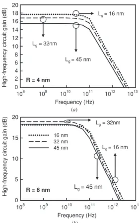
the circle plotted here is merely for a reference, which is the result of the dropped device due to its unsatisfied short-channel effect. The offset voltage of the input signal in this study is 0.6 V and the associated voltage amplifications are extracted as shown in the insets of figures5(a) and (b). The voltage amplifications are then transferred into the dc circuit gain, as plotted in figure 6, where the circle denotes the dropped device with insufficient dc characteristics. As the device gate length is scales down, the transconductance of the device is increased and then increases the dc circuit gain. However, the device with such radius and channel length possesses a small aspect ratio which degrades the device performance. The high-frequency responses of the 4 and 6 nm radius nanowire FET circuits are explored as shown in figure7; the high-frequency
10 15 20 25 30 35 40 45 50 15 16 17 18 19 20 Lg(nm) R = 4 nm R = 6 nm
High-frequency circuit gain (dB) 80x10910 15 20 25 30 35 40 45 50
100x109 120x109 140x109 160x109 180x109 200x109 220x109 Lg(nm) 3dB bandwidth (Hz) R = 4 nm R = 6 nm 10 15 20 25 30 35 40 45 50 1x10¹² 2x10¹² 3x10¹² 4x10¹² 5x10¹² 6x10¹² 7x10¹² Lg(nm) Unity-gain bandwidth (Hz) R = 4 nm R = 6 nm (a) (b) (c)
Figure 8. (a) The high-frequency circuit gain, (b) 3 dB bandwidth and (c) unity-gain bandwidth of the studied silicon nanowire circuits.
The circle appearing in (a) has the same explanation as in figure6.
108 109 1010 1011 1012 1013 0 2 4 6 8 10 12 14 16 18 20 Frequency (Hz) Lg= 32nm Lg= 16 nm Lg= 45 nm R = 4 nm
High-frequency circuit gain (dB)
108 109 1010 1011 1012 1013 0 5 10 15 20 16 nm 32 nm 45 nm Lg= 32nm Lg= 16 nm Lg= 45 nm Frequency (Hz)
High-frequency circuit gain (dB) R = 6 nm
(a)
(b)
Figure 7. High-frequency responses of the studied nanowire circuit
Semicond. Sci. Technol. 24 (2009) 045004 Y Li and C-H Hwang 108 109 1010 1011 1012 1013 0 5 10 15 20 25 30 Frequency (Hz) Planar MOSFET (Lg= 16nm) Nanowire FET (R = 4 nm; Lg= 16 nm)
High-frequency circuit gain (dB)
Figure 9. Comparison of high-frequency response for the studied
nanowire FET (4 nm radius and 16 nm gate) and the planar MOSFET with 16 nm gate, where the solid line shows the nanowire FET and the dashed line shows the planar MOSFET.
characteristics, such as high-frequency circuit gain, 3 dB bandwidth and unity-gain bandwidth, are then investigated, as shown in figures8(a)–(c), respectively. The characteristic of the high-frequency circuit gain for the studied nanowire FET circuits, as shown in figure 8(a), is similar to the dc circuit gain. The result shows that the nanowire device with larger radius and smaller gate length may exhibit higher circuit gain than those with small radius and large gate length. The 3 dB bandwidth and the unity-gain bandwidth of the circuit are proportional to [Cg(R1/ro)−1]−1and gmCg−1, respectively, and
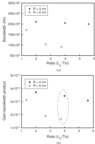
therefore the nanowire device with smaller radius may exhibit a higher 3 dB bandwidth and unity-gain bandwidth than that with larger radius as displayed in figures8(b) and (c). The high-frequency response of the nanowire FET with the largest unity-gain bandwidth (4 nm radius and 16 nm gate) is compared with that of an experimentally calibrated 16 nm gate planar MOSFET [40], as shown in figure9. To compare the device characteristic with the same operation condition, both the threshold voltages of the studied planar and nanowire devices are carefully calibrated to 380 mV. The preliminary result shows that for a well-designed 16 nm nanowire FET circuit, the gain, the 3 dB bandwidth and the unity-gain bandwidth are 20 dB, 210 GHz and 6.5 THz, respectively, which are 2.3, 8.2 and 203 times larger than those of the planar MOSFET circuits. The simulation result confirms the excellent high-frequency characteristics of the silicon nanowire FET circuit. The bandwidth and gain–bandwidth product as a function of the device aspect ratio are studied in figures 10(a) and (b), respectively. It is found that, according to the computed result, the aspect ratio of a device should be kept small enough to obtain a wider 3 dB bandwidth and a larger gain–bandwidth product, which is contrary to the demand of aspect ratio for maintaining satisfied dc characteristics as aforementioned in figure4. Moreover, the devices with smaller radii may exhibit a wider 3 dB bandwidth and a larger gain– bandwidth product even if they have a similar aspect ratio, as circled in figure 10(b). Therefore, to compromise both the dc and high-frequency characteristics, the design margin of the device aspect ratio should be restricted. Figure11plots
Ratio (L g/ Tsi) 1 2 3 4 5 6 Bandwidth (Hz) 50x109 100x109 150x109 200x109 250x109 300x109 R = 4 nm R = 6 nm Ratio (Lg/Tsi) 1 2 3 4 5 6 Gain-bandwidth product 1x10¹² 2x10¹² 3x10¹² 4x10¹² 5x10¹² R = 4 nm R = 6 nm (a) (b)
Figure 10. The (a) bandwidth and (b) gain–bandwidth product of
the nanowire FETs as a function of the aspect ratio.
Ratio (Lg/Tsi) 1 2 3 4 5 6 S.S. (mV/dec) 60 62 64 66 68 70 72 74 76 Gain-Bandwidth Product 3.0x10¹² 3.5x10¹² 4.0x10¹² S.S.= 75 mV/dec Gain-bandwidth = 3.5x10¹² Design Margin R = 4
Figure 11. The design margin of the device aspect ratio for
pursuing a device with a subthreshold swing smaller than 75 mV/dec and gain–bandwidth product larger than 3.5× 10¹².
the dependence of the device aspect ratio on dc and high-frequency characteristics. If we are pursuing a device with preferable immunity from the short-channel effect, such as the subthreshold swing within 75 mV/dec, the aspect ratio of the device should be larger than 2. However, if high gain– bandwidth product is required, say larger than 3.5 × 10¹², the device aspect ratio should be smaller than 3.5. Consequently, the requirements of dc and high-frequency characteristics may result in upper and lower bounds of the device aspect ratio, respectively. Moreover, the design margin will be more tightened for a device with larger radius due to the worse channel controllability-induced degradation of dc and 6
high-frequency characteristics. From the manufacturability point of view, the design of a silicon nanowire transistor is more restricted and complex to meet the specification of dc and high-frequency characteristics.
4. Conclusions
In this paper, the dc baseband and high-frequency characteristics and the design of the nanoscale silicon nanowire FET with 100% surrounding gate have been numerically studied using a calibrated 3D device/circuit coupled mixed-mode simulation. For a well-designed nanoscale nanowire FET, the unity-gain bandwidth can be greater than 6.5 THz; moreover, the high-frequency circuit gain, the 3 dB bandwidth and the unity-gain bandwidth of the silicon nanowire circuit are 2.3, 8.2 and 203 times larger than those of the planar MOSFET circuits. In design of silicon nanowire FETs, the demands of aspect ratio on dc and high-frequency characteristics are inversely proportional, and therefore the design margin of the device aspect ratio should be restricted to compromise the dc and high-frequency characteristics. A margin of the device aspect ratio from 2 to 3.5 has been found in this work; with the degradation of channel controllability for a device with larger radius, the design margin is more tightened. This study has shown fascinating dc baseband and high-frequency properties of silicon nanowire FET devices as active components in microwave circuits, compared with planar CMOS devices. Complete derivation of the analytical expressions of the maximum transconductance, the output resistance, the gate capacitance, dc gain and high-frequency properties for the silicon nanowire FET circuit should be investigated in future work.
Acknowledgment
This work was supported by Taiwan National Science Council (NSC) under contract NSC-97-2221-E-009-154-MY2 and NSC-96-2221-E-009-210.
References
[1] Li Y and Chou H-M 2005 A comparative study of electrical characteristic on sub-10 nm double gate MOSFETs IEEE
Trans. Nanotechnol.4 645–7
[2] Li Y and Hwang C-H 2007 Electrical characteristic
fluctuations in 16 nm bulk-FinFET devices Microelectron.
Eng.84 2093–6
[3] Li Y and Hwang C-H 2007 Effect of fin angle on electrical characteristics of nanoscale round-top-gate bulk FinFETs
IEEE Trans. Electron Devices54 3426–9
[4] Yu B et al 2002 FinFET scaling to 10 nm gate length Int.
Electron Devices Meeting (San Francisco, 8–11 December 2002) pp 251–4
[5] Suk S D et al 2008 High-performance twin silicon nanowire MOSFET (TSNWFET) on bulk Si wafer IEEE Trans.
Electron Device 7 181–4
[6] Fischetti M V 2003 Scaling MOSFET’s to the limit: a physicists’s perspective J. Comput. Electron2 73–9 [7] Yu Y S, Lee S H, Oh J H, Kim H J, Hwang S W and Ahn D
2008 A compact analytical current conduction model for a depletion-mode n-type nanowire field-effect transistor with a bottom-gate structure Semicond. Sci. Technol.23 035025
[8] Xiong S and Bokor J 2003 Sensitivity of double-gate and FinFET devices to process variations IEEE Trans. Electron
Device50 2255–61
[9] Nair P R and Alam M A 2007 Design considerations of silicon nanowire biosensors IEEE Trans. Electron Device
54 3400–8
[10] Chau R, Datta S, Doczy M, Doyle B, Jin B, Kavalieros J, Majumdar A, Metz M and Radosavljevic M 2005 Benchmarking nanotechnology for high-performance and low-power logic transistor applications IEEE Trans.
Nanotechnol.4 153–8
[11] Balaban S N, Pokatilov E P, Fomin V M, Gladilin V N, Devreese J T, Magnus W and Schoenmaker W 2002 Quantum transport in a cylindrical sub-0.1 μm silicon-based MOSFET Solid State Electron.46 435–44 [12] Li Y, Hwang C-H and Huang H-M 2008 Large-scale atomistic
approach to discrete-dopant-induced characteristic fluctuations in silicon nanowire transistors Phys. Status
Solidi a 205 1505–10
[13] Yang F-L et al 2002 25 nm CMOS omega FETs Int. Electron
Devices Meeting (San Francisco, 8–11 December 2002)
pp 255–8
[14] Monfray S et al 2002 50 nm-gate all around (GAA)-silicon on nothing (SON)-devices: a simple way to co-integration of GAA transistors within bulk MOSFET process Dig. Tech.
Pap. Symp. VLSI (Honolulu, 11–13 June 2002) pp 108–9
[15] Bindal A, Naresh A, Pearl Y, Nguyen K K and
Hamedi-Hagh S 2007 The design of dual work function CMOS transistors and circuits using silicon nanowire technology IEEE Trans. Nanotechnol.6 291–302 [16] Lazaro A and Iniguez B 2006 RF and noise performance of
multiple-gate SOI MOSFETs European Microwave
Integrated Circuits Conf. (Manchester, 10–13 September 2006) pp 312–5
[17] Cho K H, Suk S D, Yeoh Y Y, Li M, Yeo K H, Kim D-W, Hwang S W, Park D and Ryu B-I 2006 Observation of single electron tunneling and ballistic transport in twin silicon nanowire MOSFETs (TSNWFETs) fabricated by top-down CMOS process Int. Electron Devices Meeting
(San Francisco, 11–13 December 2006) pp 1–4
[18] Marchi A, Gnani E, Reggiani S, Rudan M and Baccarani G 2006 Investigating the performance limits of silicon-nanowire and carbon-nanotube FETs Solid-State Electron. 50 78–85
[19] Li Y, Lee J-W and Chou H-M 2004 Silicon–germanium structure in surrounding-gate strained silicon nanowire field effect transistors J. Comput. Electron.3 251–5
[20] Li Y, Chou H-M and Lee J-W 2005 Investigation of electrical characteristics on surrounding-gate and omega-shaped-gate nanowire FinFETs IEEE Trans. Nanotechnol.4 510–6 [21] Yang F-L et al 2004 5 nm-gate nanowire FinFET Dig. Tech.
Pap. Symp. VLSI (Hawaii, 15–17 June 2004) pp 196–7
[22] Lederer D, Kilchytska V, Rudenko T, Collaert N, Flandre D, Dixit A, Meyerd K D and Raskin J-P 2005 FinFET analogue characterization from DC to 110 GHz Solid-State
Electron.49 1488–96
[23] Jimenez D, Iniguez B, Sune J, Marsal L F, Pallares J, Roig J and Flores D 2004 Continuous analytic I–V model for surrounding-gate MOSFETs IEEE Electron Device Lett. 25 571–3
[24] Kumar M-J, Orouji A-A and Dhakad H 2006 New dual-material SG nanoscale MOSFET: analytical threshold-voltage model IEEE Trans. Electron Device 53 920–2
[25] Gnani E, Reggiani S, Rudan M and Baccarani G 2006 Design considerations and comparative investigation of ultra-thin SOI, double-gate and cylindrical nanowire FETs Proc.
European Solid-State Dev. Res. Conf. (Montreux, 19–21 September 2005) pp 371–4
Semicond. Sci. Technol. 24 (2009) 045004 Y Li and C-H Hwang [26] Paul B C, Ryan T, Fujita S, Okajima M, Lee T H and Nishi Y
2007 An analytical compact circuit model for nanowire FET IEEE Trans. Electron Device54 1637–44 [27] Yamamoto Y, Hidaka T, Nakamura H, Sakuraba H
and Masuoka F 2006 Decananometer surrounding gate transistor (SGT) scalability by using an intrinsically-doped body and gate work function engineering IEICE Trans.
Electron. E89-C 560–7
[28] Grasser T and Selberherr S 2000 Mixed-mode device simulation Microelectron. J.31 873–81
[29] Li Y 2007 A two-dimensional thin-film transistor simulation using adaptive computing technique Appl. Math. Comput. 184 73–85
[30] Huang K-Y, Li Y and Lee C-P 2003 A time-domain approach to simulation and characterization of RF HBT two-tone intermodulation distortion IEEE Trans. Microwave Theory
Tech.51 2055–62
[31] Li Y, Huang J-Y and Lee B-S 2008 Effect of single grain boundary position on surrounding-gate polysilicon thin film transistors Semicond. Sci. Technol.23 015019
[32] Li Y and Huang K-Y 2003 A novel numerical approach to heterojunction bipolar transistor circuit simulation Comput.
Phys. Commun.152 307–16
[33] Ancona M G and Tiersten H F 1987 Macroscopic physics of the silicon inversion layer Phys. Rev. B35 7959–65 [34] Odanaka S 2004 Multidimensional discretization of the
stationary quantum drift-diffusion model for ultrasmall MOSFET structures IEEE Trans. Comput.-Aided Des.
Integr. Circuits Syst.23 837–42
[35] Tang T-W, Wang X and Li Y 2002 Discretization scheme for the density-gradient equation and effect of boundary conditions J. Comp. Electron.1 389–93
[36] Munteanu D, Autran J L, Ferlet-Cavrois V, Paillet P, Baggio J and Castellani K 2007 3D quantum numerical simulation of single-event transients in multiple-gate nanowire MOSFETs IEEE Trans. Nucl. Sci. 54 994–1001
[37] Li Y and Yu S-M 2005 A parallel adaptive finite volume method for nanoscale double-gate MOSFETs simulation
J. Comput. Appl. Math.175 87–99
[38] Li Y, Lu H-M, Tang T-W and Sze S M 2003 A novel parallel adaptive Monte Carlo method for nonlinear Poisson equation in semiconductor devices Math. Comput. Simul. 62 413–20
[39] Li Y, Sze S M and Chao T-S 2002 A practical implementation of parallel dynamic load balancing for adaptive
computing in VLSI device simulation Eng. Comput. 18 124–37
[40] Li Y, Yu S-M, Hwang J-R and Yang F-L 2008 Discrete dopant fluctuated 20 nm/15 nm-gate planar CMOS IEEE Trans.
Electron Device55 1449–55
[41] Asenov A, Watling J R, Brown A R and Ferry D K 2002 The use of quantum potentials for confinement and tunnelling in semiconductor devices J. Comput. Electron. 1 503–13
[42] Watling J R, Brown A R, Asenov A, Svizhenko A and Anantram M P 2002 Simulation of direct source-to-drain tunnelling using the density gradient formalism: non-equilibrium Greens function calibration
Proc. Int. Simulation of Semiconductor Processes and Devices Conf. (Kobe, Japan, 4–6 September 2002)
pp 267–70
[43] Razavi B 2001 Design of Analog CMOS Integrated Circuits (New York: McGraw-Hill)