Correlation Between Electrical Characteristics and
Oxide
ÕPolysilicon Interface Morphology for
Excimer-Laser-Annealed Poly-Si TFTs
Ching-Lin Fanzand Mao-Chieh Chen*
Department of Electronics Engineering and Institute of Electronics, National Chiao-Tung University, Hsinchu 300, Taiwan
This work investigates the correlation between electrical characteristics and gate-oxide/polysilicon interface morphology for excimer-laser-annealed共ELA兲 poly-Si thin-film transistors 共TFTs兲. The main feature of ELA poly-Si films is protrusion at grain boundaries that makes the film surface appear very rough. The surface roughness increases with increasing laser energy density and causes degradation of off-current and reliability for the ELA poly-Si TFTs. This degradation of the off-current is attributed to the lower channel resistance due to the increase in crystallinity of the poly-Si layer and the enhancement of localized electric field arising from the protrusions at the grain boundaries. In addition, the increase of localized electric field also degrades device reliability. Passivation of gate oxide/poly-Si channel by NH3-plasma treatment was found to be favorable in improving the performance and reliability of the ELA poly-Si TFTs.
© 2002 The Electrochemical Society. 关DOI: 10.1149/1.1504721兴 All rights reserved.
Manuscript submitted November 8, 2001; revised manuscript received March 26, 2002. Available electronicallyAugust 21, 2002.
Low-temperature processed 共LTP兲 polycrystalline silicon thin-film transistors共poly-Si TFTs兲 are attracting much attention for use in active matrix liquid crystal displays共AMLCDs兲 because of their higher field-effect mobility and driving current compared to amor-phous silicon TFTs currently used for large-area electronics.1Thus, integration of the AMLCD and its peripheral driver circuits on a single glass substrate is of great advantage for the LTP poly-Si TFTs. In order to fabricate LTP poly-Si TFTs on a glass substrate, all of the fabrication processes must be carried out at low temperatures of no more than 600°C.
It is well known that excimer laser annealing共ELA兲 is a very promising scheme for the crystallization of amorphous silicon be-cause the laser process heats thin silicon films to the melting point on several tens of nanoseconds that allows the films to melt and recrystallize without significantly heating the glass substrate. More-over, it has been reported that ELA resulted in high-quality polysili-con films with very few intragrain defects, leading to significant improvement in the electrical characteristics of poly-Si TFTs.2-5 However, during the phase transformation from liquid to solid in the laser crystallization, many protrusions are formed at the oxide/ polysilicon interface, causing a very rough surface of polysilicon.6 The enhanced electric field arising from the asperities at the rough surface led to adverse effects on the electrical characteristics and also created reliability problems in the ELA poly-Si TFTs.7,8 The surface roughness inherent to the ELA process has been a trouble-some problem. In recent years, many investigations have been re-ported regarding the formation mechanism of protrusions and the reduction scheme of the surface roughness,5,6,9-11 whereas little study has been made with respect to the correlation between device behavior and interface morphology for the ELA poly-Si TFTs.12In this study, correlation between electrical characteristics and oxide/ polysilicon interface morphology of the ELA poly-Si TFTs is inves-tigated, in particular, the off-state characteristics and device reliabil-ity. In addition, the study also includes the effects of NH3-plasma treatment on the ELA poly-Si TFTs.
Experimental
Self-aligned top-gated n-channel ELA poly-Si TFTs were fabri-cated on thermal oxide-covered silicon wafers according to the fol-lowing procedures. A 110 nm thick low-pressure chemical vapor deposited共LPCVD兲 amorphous Si layer was first deposited using a SiH4process at 550°C. All specimens were then irradiated by KrF
excimer laser beam ( ⫽ 248 nm) with various energy densities at room temperature in a vacuum ambient (⬃10⫺3Torr). The excimer laser beam had a pulse duration of 15 ns and a pulse repetition rate of 20 Hz. An optical homogenizer produced a 1.8⫻ 23 mm shaped profile on the surface of the irradiated specimen. The line-shaped profile scanned the whole surface area of the substrate with a 98% overlap ratio per each laser shot, so that every part on the silicon film was irradiated 50 times by the excimer laser light with the same energy density. After the laser annealing, the silicon film was patterned into individual active device islands, and a 120 nm thick plasma-enhanced chemical vapor deposited 共PECVD兲 tetra-ethyl orthosilicate共TEOS兲 oxide was deposited at 300°C to serve as the gate insulator. A second LPCVD poly-Si film was subsequently deposited and patterned using dry reactive ion etching共RIE兲 to form the gate electrode. Next, the source/drain and gate regions were doped with phosphorus via self-aligned P⫹ion implantation at an energy of 40 keV to a dose of 5⫻ 1015cm⫺2, followed by a ther-mal annealing at 600°C for 24 h in an N2ambient. Then, a 500 nm thick PECVD-TEOS passivation oxide was deposited at 300°C. Af-ter the contact holes were opened, metallization of Al electrodes was completed, followed by a sintering process at 400°C for 30 min in an N2 ambient. For comparison, control samples were also fabri-cated following the same process except that the ELA was replaced by a solid-phase crystallization 共SPC兲 conducted in a furnace at 600°C for 24 h in an N2ambient. In addition, a group of TFTs was subjected to NH3-plasma hydrogenation at 300°C in a parallel-plate reactor with a power density of 0.7 W/cm2in order to investigate the passivation effect of NH3plasma on the electrical characteristics of ELA poly-Si TFTs. In this study, all devices investigated have a gate width/length dimension of 50/10m.
The images of the oxide/polysilicon interface morphology of the poly-Si TFTs were measured using scanning electron microscopy 共SEM兲 and atomic force microscopy 共AFM兲. The I-V characteristics of the fabricated devices were measured using an HP4145B semi-conductor parameter analyzer. Various device parameters, including the threshold voltage (VTH), the subthreshold swing 共S.S.兲, the maximum on-current (ION), and the minimum off-current (IOFF) were measured at a drain voltage of VDS⫽ 5 V. The threshold volt-age is defined as the gate voltvolt-age which yields a drain current (IDS) of 500 nA (IDS⫽ 100 nA ⫻ W/L). The field-effect mobility (FE) is calculated from the maximum value of the transconductance at VDS⫽ 0.1 V. The maximum and minimum values of IDS at VDS ⫽ 5 V are designated as IONand IOFF, respectively.
*Electrochemical Society Active Member.
zE-mail: [email protected]
Journal of The Electrochemical Society, 149共10兲 G567-G573 共2002兲 0013-4651/2002/149共10兲/G567/7/$7.00 © The Electrochemical Society, Inc.
Results and Discussion
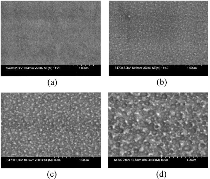
Oxide/polysilicon interface morphology.— Figure 1 illustrates the SEM images of silicon films crystallized by excimer laser irra-diation with various energy densities. It can be seen clearly that the larger the irradiated laser energy density is, the higher the localized protrusion is formed, making the film surface rougher. During the laser irradiation on the ␣-Si layer, significant mass transport oc-curred toward the grain boundaries due to the very short solidifica-tion period of the melted silicon films. The 10% density change between the solid and liquid phases of silicon provides a driving force for the creation of capillary waves, and hence, the solidifying silicon expands and exerts a positive force on the adjacent melt. Thus, during the solidification, grains grow laterally and push the liquid silicon toward the growth direction. In the final stage of so-lidification, when two growing grains meet to form the grain bound-ary, protrusion is developed because liquid silicon has a larger den-sity than solid silicon. Where two grains meet to form a grain boundary, a ridge develops. In addition, where three or more grains meet to form a vertex, a hillock may develop.5,6Figure 1 shows that surface roughness always accompanies the formation of grain boundaries, forming shallow valleys in the grains and large hillocks
at the boundaries. Although the grain boundaries are invisible in Fig. 1, the protrusions are the consequence of the existing grain bound-aries, as reported in the literature.
AFM was used to evaluate the surface roughness of silicon films. Figure 2 illustrates the AFM images of poly-Si films obtained by SPC and ELA with various energy densities. The results of AFM are consistent with and complementary to those of SEM. Poly-Si films grown directly by LPCVD usually lead to the formation of tooth-like-shaped grains with valleys appearing at the grain boundaries.13 This is different from the ELA poly-Si films, where the relative height of hillocks at the boundaries to valleys in the grains causes the asperity of polysilicon surface. Irradiation with low LED re-sulted in smooth surfaces; however, as the LED increased, the sur-face roughness also increased due to the ridge and/or hillock forma-tion. Figure 3 shows the root-mean-square 共rms兲 value of surface roughness Rrmsvs. irradiated LED with data of the SPC poly-Si film included for comparison. A change in surface roughness increasing rate is found to occur at LED of 160 mJ/cm2. This turnaround LED is consistent with the energy density of surface melting (ESM) re-ported in literature.5Below the turnaround LED, the silicon film is almost unmolten during the irradiation, causing only slight change
Figure 1. SEM micrographs showing surface morphologies of Si films crystallized by excimer laser irradiation with various energy densities:共a兲 as-deposited
in surface roughness with LED; however, above the turnaround LED, the silicon film is partially or completely melted, depending on the irradiated LED, and crystallized by the liquid-phase crystal-lization, resulting in the rapid increase in surface roughness with increasing LED. It was reported that the microstructure of the ELA poly-Si films is clearly stratified with a large-grain layer on the surface and the underlying fine-grain material. The large-grain ma-terial corresponds to the crystallization from the molten phase and the underlying fine-grain material corresponds to the explosive crystallization.14,15As the LED increases, the melting depth is also increased to result in downward extension of the large-grain region toward the poly-Si/substrate interface, forming even larger grains. At the same time, a larger amount of liquid silicon is pushed toward the grain boundaries as a result of an increase in grain size with increasing LED,6,14causing the formation of a higher ridge and/or hillock and thus an increase in surface roughness, as shown in Fig. 3.
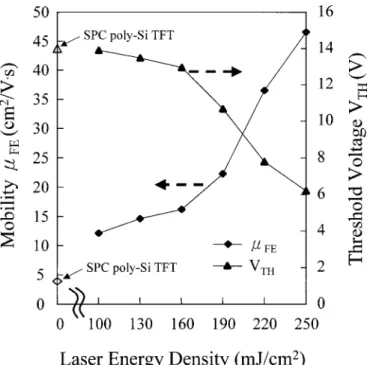
Electrical characteristics of ELA poly-Si TFTs.— Figure 4 shows the typical transfer characteristics (IDS-VGS) of the ELA poly-Si TFTs with various共LEDs兲. It is found that the device characteristics are significantly affected by the irradiated LED. Figure 5 shows the field-effect mobility (FE) and the threshold voltage (VTH) vs. irra-diated LED for the ELA poly-Si TFTs. TheFEincreases with LED while the VTHdecreases with LED; this is because an increase in the irradiated LED results in an increase in the grain size, causing a decrease in the number of grain boundaries16,17and hence a decreas-ing trap state density. Figure 6 shows the activation energy (Ea) of drain current vs. gate voltage (VGS), measured at VDS⫽ 0.1 V, for
Figure 2. AFM images of Si films
crys-tallized by SPC and ELA with various energy densities:共a兲 SPC at 600°C for 24 h,共b兲 ELA with 160 mJ/cm2,共c兲 ELA with 190 mJ/cm2, and共d兲 ELA with 250 mJ/cm2.
Figure 3. RMS value of surface roughness Rrmsvs. irradiated LED. Data of SPC poly-Si film is included for comparison.
the ELA poly-Si TFTs irradiated with different LEDs. The activation energy of drain current can be derived from the Arrhenius plot of drain current, and the value of Eareflects the carrier transport barrier of the grain boundary within the poly-Si channel.18The lower the Ea is, the lower the carrier transport barrier of the grain boundary will be. A lower transport barrier implies a lower trap state density. Thus,
irradiation with a higher LED would result in a lower Eaand hence, lower trap state density, leading to improvement of the device per-formance, as shown in Fig. 4-6.
The off-current (IOFF) vs. irradiated LED for the ELA poly-Si TFTs is illustrated in Fig. 7. It is found that the IOFFincreases with increasing LED, similar to two reports in the literature14,19but con-tradictory to another report.17It is well known that TFTs with high off-current degrade the contrast ratio of display because of the loss of video information before the frame is being refreshed. Thus, a low off-current is necessary to hold the signal level for an acceptable image quality.20Since there is a similar tendency of increasing off-current (IOFF) and surface roughness (Rrms) with respect to the in-creasing LED共Fig. 7 and 3兲, we presume that some sort of a corre-lation should exist between the oxide/polysilicon interface morphology and the off-current of the ELA poly-Si TFTs.
It has been reported that the off-current in the LTP poly-Si TFTs is composed of two components: the resistive current in the low-gate-bias region and the junction leakage current in the high-gate-bias region.21,22The resistive current is controlled by the channel resistance, which in turn is related to the crystallinity of the poly-Si channel layer. The better the crystallinity of the poly-Si channel layer is, the lower the channel resistance will be. Since roughness of the poly-Si layer increases with increasing LED, we presume that the resistive current also increases with increasing LED, because the increase of surface roughness implies the increasing crystallinity of the poly-Si layer. The junction leakage current is known to be con-trolled by the emission of trapped carriers in the potential wells at the grain boundaries. In the negative high-gate-bias region, the ap-plied reverse gate bias causes the potential barrier to be so thin that the tunneling of trapped carriers to the conduction band, directly or intermediately via trap states, occurs very frequently. Thus, the junc-tion leakage current is closely correlated with the high reverse gate bias. Since the poly-Si surface roughness increases with increasing LED, the localized electric field will be further enhanced by the poly-Si surface asperity arising from the protrusions at the grain
Figure 4. Typical transfer characteristics (IDS⫺ VGS) of ELA Poly-Si TFTs irradiated with various LEDs.
Figure 5. Field-effect mobility (FE) and threshold voltage (VTH) vs. irra-diated LED for the ELA poly-Si TFTs. Data of SPC poly-Si TFT are in-cluded for comparison.
Figure 6. Activation energies (Ea) of drain current vs. gate voltage (VGS), measured at VDS⫽ 0.1 V, for the ELA poly-Si TFTs irradiated with differ-ent LEDs.
boundaries with the increasing LED. As a result, tunneling of trapped carriers to the conduction band is enhanced, leading to the increase of junction leakage current in the high-gate-bias region with increasing LED. This correlation between the oxide/polysilicon interface morphology and the off-current of the ELA poly-Si TFTs clearly explains the observation in this work that both the interface roughness and the off-current increased with increasing LED.
Figure 8 shows the on-current degradation as a function of stress time under a stress voltage of VGS⫽ 30 V for the ELA poly-Si TFTs irradiated with different LEDs. The percent degradation of on-current ⌬ION is defined as ⌬ION(%) ⫽ 关(ION after stress ⫺ IONbefore stress兲/ION before stress兴 ⫻ 100%. It is found that the on-current degradation increased with the stress time; moreover, the degradation increased with increasing LED. With an externally applied gate bias, localized electric field in the oxide is enhanced by the asperity at the oxide/poly-Si interface;8 this en-hanced high electric field may generate electron traps distributed throughout the bulk of the SiO2.23Thus, when a high gate-stressing voltage is applied, electrons are injected from the channel region into the oxide layer and may subsequently be trapped into the oxide electron traps, resulting in the degradation of on-current. Since the poly-Si surface roughness共i.e., asperity兲 increases with increasing LED, localized electric field in the oxide also increases with increas-ing LED. As a result, the on-current degradation increases with in-creasing LED.
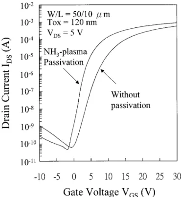
Passivation effect of NH3-plasma.—We have found that increas-ing LED resulted in an increase of off-current as well as degradation of device reliability. Thus, NH3-plasma treatment was performed on the ELA poly-Si TFTs to improve the device electrical characteris-tics. Figure 9 shows the typical transfer characteristics (IDS ⫺ VGS) of the ELA共with 250 mJ/cm2LED兲 poly-Si TFTs with and without an NH3-plasma passivation for 3 h. Obvious improvement in device performance was obtained by the NH3-plasma treatment, in particular, the off-current. This is attributed presumably to the passivation of the trap states at the SiO2/poly-Si interface and in the
poly-Si channel by the dissociated nitrogen and hydrogen radicals.24 The measured as well as extracted key device parameters are sum-marized in Table I. It is found that larger improvement in VTHand S.S. was obtained by the NH3-plasma passivation, while the
im-Figure 7. Off-current (IOFF) vs. irradiated LED for the ELA poly-Si TFTs. Data of SPC poly-Si TFT is included for comparison.
Figure 8. On-current degradation vs. stress time under a stress voltage of
VGS⫽ 30 V for the ELA poly-Si TFTs irradiated with various LEDs.
Figure 9. Typical transfer characteristics (IDS⫺ VGS) of the ELA共250 mJ/cm2LED兲 poly-Si TFTs with and without an NH3-plasma passivation for 3 h.
midgap states located at the grain boundaries, which are related closely to VTHand S.S., have a faster response to the hydrogenation, while the intragranular tail states that are related closely to FE respond slowly to the hydrogenation.25Since the ELA crystallized poly-Si film generally consists of a very low density of intragranular tail states共inside the grains兲, defects located at the grain boundaries dominate the devices’ electrical characteristics. Presumably, the poly-Si channel of the ELA poly-Si TFTs studied in this work still contain a few intragranular tail states, which are closely related to theFE; thus, the improvement inFEis of a smaller degree com-pared to that of VTHand S.S. by the NH3-plasma treatment. Figure 10 shows the on-current degradation as a function of stress time under a stress voltage of VGS⫽ 30 V for the ELA poly-Si TFTs 共irradiated with 250 mJ/cm2laser energy density兲, with and without an NH3-plasma passivation. It is found that the on-current degrada-tion under a high voltage stress was greatly alleviated by the NH3-plasma passivation. We attribute this improvement to the effect of nitrogen radicals in the oxide. It was reported that there are many strained bonds within the polyoxide, especially at local regions in the vicinity of the grain boundaries.26These strained bonds are eas-ily broken by high-energy electrons when a high electric field is
closely related to the poly-Si surface roughness. Enhanced protru-sions at grain boundaries as a result of increasing LED increase the poly-Si surface roughness and thus the crystallinity of the poly-Si layer, leading to the increase of resistive current at low gate bias. With increasing LED, the asperities arising from the protrusions at grain boundaries also enhance the localized electric field, leading to the enhancement of trapped carrier tunneling to the conduction band, and thus the increasing of junction leakage current at high gate bias. The degradation of the devices on-current (ION) under a high-voltage stress also deteriorates with increasing LED, because the increasing localized electric field in the oxide enhanced by the as-perity at the oxide/poly-Si interface leads to generation of increasing amount of trap states in the oxide. Nevertheless, the device perfor-mance and reliability can be significantly improved by NH3-plasma treatment due to the passivation effect of nitrogen radicals generated in the NH3plasma. We believe that the reduction or elimination of oxide/polysilicon interface roughness is of essential importance for the improvement of device performance for the ELA poly-Si TFTs, in particular, the off-current and reliability.
National Chiao-Tung University assisted in meeting the publication costs of this article.
References 1. J. Ohwada, SID Dig. 1986, 55.
2. T. Sameshima, S. Usui, and M. Sekiya, IEEE Electron Device Lett., EDL-7, 276
共1986兲.
3. R. F. Wood and G. E. Giles, Phys. Rev. B, 32, 2923共1981兲.
4. R. Carluccio, J. Stoemenos, G. Fortunato, D. B. Meakin, and M. Bianconi, Appl. Phys. Lett., 66, 1394共1995兲.
5. M. Miyasaka and J. Stoemenos, J. Appl. Phys., 86, 5566共1999兲.
6. D. K. Fork, G. B. Anderson, J. B. Boyce, R. I. Johnson, and P. Mei, Appl. Phys. Lett., 68, 2138共1996兲.
7. A. Rahal, T. M. Brahim, H. Toutah, B. T. Ighil, Y. Helen, C. Prat, and F. Raoult, Microelectron. Reliab., 39, 851共1999兲.
8. B. Y. Chan, C. T. Nguyen, P. K. Ko, T. Y. Chan, and S. S. Wong, IEEE Trans. Electron Devices, ED-44, 455共1997兲.
9. D. J. McCulloch and S. D. Brotherton, Appl. Phys. Lett., 66, 2060共1995兲. 10. A. Marmorstein, A. T. Voutsas, and R. Solanki, J. Appl. Phys., 82, 4303共1997兲. 11. D. Toet, P. M. Smith, T. W. Sigmon, T. Takehara, C. C. Tsai, W. R. Harshbarger,
and M. O. Thompson, J. Appl. Phys., 85, 7914共1999兲.
12. M. Kimura, T. Eguchi, S. Inoue, and T. Shimoda, Jpn. J. Appl. Phys., Part 2, 39, L775共2000兲.
13. C. A. Dimitriadis, J. Stoemenos, P. A. Coxon, S. Friligkos, J. Antonopoulos, and N. A. Economou, J. Appl. Phys., 73, 8402共1993兲.
14. S. D. Brotherton, D. J. McCulloch, J. B. Clegg, and J. P. Gowers, IEEE Trans. Electron Devices, ED-40, 407共1993兲.
15. M. O. Thompson, G. J. Galvin, and J. W. Mayer, Phys. Rev. Lett., 52, 2360共1984兲. 16. J. S. Im and H. J. Kim, Appl. Phys. Lett., 63, 1969共1993兲.
17. G. K. Giust and T. W. Sigmon, IEEE Trans. Electron Devices, ED-45, 925共1998兲. 18. B. A. Khan and R. Pandya, IEEE Trans. Electron Devices, ED-37, 1727共1990兲. 19. T. Aoyama, Y. Koike, Y. Okajima, N. Konishi, T. Suzuki, and K. Miyata, IEEE
Trans. Electron Devices, ED-38, 2058共1991兲.
20. A. Chiang, I. W. Wu, M. Hack, A. G. Lewis, T. Y. Huang, and C. C. Tsai, Extended Abstracts of the 1991 Conference on Solid State Devices and Materials, Japan, p. 586.
21. C. F. Yeh, S. S. Lin, T. Z. Yang, C. L. Chen, and Y. C. Yang, IEEE Trans. Electron Devices, ED-41, 173共1994兲.
22. C. T. Angelis, C. A. Dimitriadis, I. Samaras, J. Brini, G. Kamarinos, V. K. Gue-orguiev, and Tz. E. Ivanov, J. Appl. Phys., 82, 4095共1997兲.
Figure 10. On-current degradation vs. stress time under a stress voltage of
VGS⫽ 30 V for the ELA poly-Si TFTs 共with 250 mJ/cm2LED兲 with and without NH3-plasma passivation.
23. C. A. Dimitriadis and P. A. Coxon, Appl. Phys. Lett., 54, 620共1989兲.
24. F. S. Wang, M. J. Tsai, and H. C. Cheng, IEEE Electron Device Lett., EDL-16, 503
共1995兲.
25. I. W. Wu, T. Y. Huang, W. B. Jackson, A. G. Lewis, and A. Chiang, IEEE Electron Device Lett., EDL-12, 181共1991兲.
26. A. Shintani and H. Nakashima, Appl. Phys. Lett., 36, 983共1980兲.
27. H. S. Momose, T. Morimoto, Y. Ozawa, K. Yamabe, and H. Iwai, IEEE Trans. Electron Devices, ED-41, 546共1994兲.
28. M. J. Tsai, F. S. Wang, K. L. Cheng, S. Y. Wang, M. S. Feng, and H. C. Cheng, Solid-State Electron., 38, 1233共1995兲.
29. C. K. Yang, T. F. Lei, and C. L. Lee, Tech. Dig. - Int. Electron Devices Meet., 1994, 505.