國 立 交 通 大 學
電子工程學系 電子研究所碩士班
碩 士 論 文
22 奈米高介電係數金屬閘極電晶體之正
向偏壓溫度不穩定性分析及模擬
Positive Bias Temperature Instability(PBTI)
Analysis and Simulation in 22 nm High-k Metal
Gate nMOSFETs
研 究 生 :王志宇
指導教授 :汪大暉 博士
中華民國 一百 年 七 月
22 奈米高介電係數金屬閘極電晶體之正
向偏壓溫度不穩定性分析及模擬
Positive Bias Temperature Instability(PBTI)
Analysis and Simulation in 22 nm High-k Metal
Gate nMOSFETs
研 究 生 : 王志宇 Student : Chih Yu, Wang
指導教授 : 汪大暉 博士 Advisor : Dr. Tahui Wang
國立交通大學
電子工程學系 電子研究所碩士班
碩士論文
A Thesis
Submitted to Department of Electronics Engineering & Institute of Electronics
College of Electrical and Computer Engineering
National Chiao Tung University
In Partial Fulfillment of the Requirements
For the Degree of Master
In
Electronic Engineering
July 2011
Hsinchu, Taiwan, Republic of China.
i
22 奈米高介電係數金屬閘極電晶體之正向偏壓
溫度不穩定性分析及模擬
學生:王志宇
指導教授:汪大暉 博士
國立交通大學 電子工程學系 電子研究所
摘要
在本篇論文中,我們提出了一個新的方法來模擬高介電係數CMOS在經 過高溫偏壓操作後截止電壓的分佈。在量測上我們使用快速暫態的量測技 術來減少量測的延遲時間,我們發現在經過高溫偏壓操作後由於電子被捕 捉使得電流發生階梯狀衰減的現象。 為了了解在高溫偏壓操作時的單電子捕捉的現象,我們首先萃取由於 電 子 被 捕 捉 時 電 流 的 衰減 量 的 機 率 分 佈, 接 著 我 們 也 建 立 了 在施 壓 (stress)及回復(recovery)時的時間模型。由以上實驗所得到的參數進行 蒙地卡羅模擬來預測經過高溫偏壓操作後截止電壓的分佈。ii
Positive Bias Temperature Instability(PBTI)
Analysis and Simulation in 22 nm High-k Metal
Gate nMOSFETs
Student: Chih Yu Wang Advisor: Dr. Tahui Wang
Department of Electronics Engineering &
Institute of Electronics
National Chiao Tung University
Abstract
In this dissertation a new method to predict the post-stress threshold voltage distribution is introduced. We proposed the fast transient measurement, which minimizes the switching delay between stress and measurement. Consequently, a staircase-like post-positive bias temperature (PBT) current instability caused by single electron trapping is investigated.
To analyze the characteristic of PBTI stress induced threshold voltage degradation. First, we extract the probability distribution of the single electron trapping induced drain current degradation. Second, the time model is developed in stress and recovery phase. According to the characterization of the single charge
iii
phenomenon, we proposed a Monte Carlo simulation to simulate the post-stress threshold voltage distribution.
iv
Acknowledgement
首先,我要感謝我的指導教授汪大暉老師,能夠提供一
個設備完善的實驗資源,老師謝心與耐心的教導使我們能夠
學習到正確的研究態度與方法。另外,博士班的邱榮標、馬
煥淇學長也是從我剛進實驗室到要畢業的現在一直在各方
面都給了我很大的幫助,使我獲益良多,實驗室同學王明緯、
周承翰還有學弟們不管在研究上以及日常生活中都帶給了
我許多支持與樂趣。
最後我要感謝我的父母以及女友,在這段期間給我的支
持鼓勵。謝謝!
v
Contents
Chinese Abstract i English Abstract ii Acknowledgement iii Contents iv Figure Captions vi Chapter 1 Introduction 1Chapter 2 Single Charge Phenomena in PBTI 4
2.1 Introduction 4
2.2 Measurement Setup 4
2.3 ΔId Distribution of PBTI 5
2.3.1 The Probability Function of ΔId in Recovery Phase 6
2.3.2 Comparison of the ΔId Distribution in Different 6
Condition
2.3.3 The Difference of ΔId Distribution between Initial 7
Trap and Stress Induced Trap
2.4 The Time Model in Stress and Recovery Phase 8 2.4.1 The Time Model in Stress Phase 8 2.4.2 The Time Model in Recovery Phase 9
2.5 Width Dependence in PBTI Recovery 11
Chapter 3 Monte Carlo Simulation of VT Distribution in PBTI
Stress
34
vi
3.2 Simulation Flow 34
3.3 Simulation of Width Dependence in PBTI Stress 35 3.4 Simulation of Device Lifetime in PBTI Stress 35
Chapter 4 Conclusion 46
vii
Figure Captions
Fig. 1.1 PBTI becomes worse in the Hf based high-k device. p.3 Fig. 2.1 Traditional method needs long measurement time and wastes lots
of devices.
p.12
Fig. 2.2 Our method is based on characterizing the single charge phenomena, in order to simulate single electron trapped in PBTI.
P.13
Fig. 2.3 The high-k/metal gate device structure used in the following experiment.
p.14
Fig. 2.4 The instrument setting in order to achieve the fast transient measurement.
p.15
Fig. 2.5 (a) A typical pattern of Id degrade in PBTI stress phase, which
cause by single electron trapping.
(b)Schematic of the constant voltage stress procedures.
p.16
Fig. 2.6 (a) A typical pattern of Id recovery in PBTI recovery phase, which
cause by single electron de-trapping.
(b)Waveforms applied to gate and drain during stress and measurement.
p.17
Fig. 2.7 To extract ΔId amplitude, we normalized ΔId with Id(fresh) for the
same criterion.
p.18
Fig. 2.8 The ΔId amplitude follows exponential distribution caused by
percolation effect.
p.19
Fig. 2.9 (a) A interface trap located at critical path would make ΔId larger.
(b) A interface trap located at a insignificant point make smaller ΔId.
p.20
Fig. 2.10 (a) Similarly, ΔId amplitude in stress phase is extracted.
(b) The ΔId distribution followed the same mechanism in stress and
recovery phase.
viii
Fig. 2.11 The ΔId distribution had no stress voltage dependence in (a) stress
and (b) recovery phase
p.22
Table2.1 The stress induced trap exhibited a larger σ. p.23 Fig. 2.12 (a) The ΔId distribution of PBTI and post-stress RTN exhibited
larger σ, which means the stress induced traps located on the critical current path.
(b) The higher probability of trap generation on the high electron density region.
p.24
Fig. 2.13 Threshold voltage shift versus stress time followed power-law of a device stressed under high gate voltage.
p.25
Fig. 2.14 The ΔVT versus stress time characteristics under three different
stress voltage.
p.26
Fig. 2.15 (a) We record the time of each electron trapped in the stress phase. (b) The number of electron trapped versus stress time followed the same power-law.
p.27
Fig. 2.16 Energy band diagram illustrating possible paths for trapped charge emission.
p.28
Fig. 2.17 Temperature dependence of emission time. p.29 Fig. 2.18 Schematic representation of gate dielectric band diagram in
recovery phase and trap positions, and the proposed model is described in detail in the text.
p.30
Fig. 2.19 The emission number with a logarithmic time dependence during recovery.
p.31
Fig. 2.20 NMOS recovery ΔVT traces in different dimensional device. p.32
Table. 2.2 A smaller device exhibited a larger σ, but when the cross-section increased more electrons are trapped in the same stress time.
ix
Fig. 3.1 Flow chart of Monte Carlo simulation for post-stress VT
distribution.
p.38
Fig. 3.2 Gaussian distribution approach is appropriate in this simulation. p.39 Fig. 3.3 (a) A random number y is applied to obtain the corresponding ΔId
according to the ΔId distribution.
(b) Using σ and the time model extract from experiment, we can simulate the step-like VT variation.
P.40
Fig. 3.4 The simulation of VT distribution under a PBTI stress (1.8V 1sec)
and after 1000sec recovery.
p.41
Fig. 3.5 Due to the result, larger device exhibits more threshold shift under the same stress condition, which because more electrons trapped.
p.42
Table. 3.1 As the result, the variation of threshold voltage is concerned not only the σ but also the number of trapped electron.
p.43
Fig. 3.6 The traditional method to estimate the device lifetime. p.44 Fig. 3.7 Evaluate the device lifetime due to the simulation of post-stress
threshold voltage distribution.
p.45
Fig. 3.8 According to the ΔId distribution is irrelevant to stress voltage, the
post-stress VT distribution is consistent due to the same VT
variation.
p.46
Fig. 3.9 As the result the device lifetime can perfectly estimate. p.47 Fig. 3.10 The number of filled electron to make VT across deadline
(0.464V) is different.
p.48
Fig. 3.11 (a)The probability distribution of the trap number. (b)The lifetime distribution transformed from (a).
p.49
Fig. 3.12 From the lifetime distribution we can estimate the failure rate of the samples under the PBTI stress.
1
Chapter 1
Introduction
Metal oxide semiconductor field effect transistors (MOSFETs) have been continuously scaled down since it was developed. Thickness of gate dielectric is required to be smaller in the progressive technology node, as the device scaled down, it reached the physical limit of conventional silicon dioxide (SiO2) MOSFETs, SiO2 is
no longer an appropriate material of gate dielectric, because of the quantum mechanical direct tunneling leakage current increase in MOSFETs with ultra-thin gate oxide [1.1], which induced standby power consumption. In order to maintain the scaling roadmap, MOSFETs with high permittivity (high-k) material and metal gate is proposed. Recently, HfO2 has been successfully integrated into CMOS as gate
dielectric. The MOSFETs with high-k/metal gate have good reliability, comparable mobility (as SiO2), and the gate leakage is greatly reduced at the same equivalent
oxide thicknesses (EOT) [1.2-1.4].
Although the technique of high-k/metal gate is regarded as a good solution of the device scaling problem, it also produced other reliability issues. Positive bias temperature instability (PBTI) is one of the serious reliability concerns [1.5]. Threshold voltage (VT) of a MOSFET is observed to shift under a positive bias with
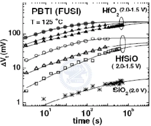
stressing time, this phenomenon which caused by single charge trapping is called PBTI [1.6-1.8]. From Fig.1.1 compare with SiO2, PBTI induced VT shift increased in
the Hafnium based high-k gate dielectric devices. It shows that the Hf plays the role of creating traps in the high-k gate dielectric stack [1.5].
2
In Chapter 2, we showed how to set an experiment with a novel transient measurement to characterizing single electron trapping in the PBTI stress phase, and the single electron emission in the PBTI recovery phase. In the stress phase the single electron trapping caused staircase-like drain current degradation, on the other hand the post-stress recovery transient of drain current in recovery phase can be measured [1.7-1.9]. Finally, the probability distribution of drain current fluctuation has been developed [1.7], also we set up the time model in the stress and recovery phase, and a comparison of different condition PBTI stress will be shown. Because of the random telegraph noise (RTN) and PBTI are both single charge effect, the difference of ΔId
probability distribution of these two mechanism is investigated. At last we showed the dimensional dependence of device in PBTI stress.
In Chapter 3, based on the probability distribution of ΔId and the time model of
PBTI stress and recovery phase in the previous chapter, we developed a new method to simulate the PBTI stress induced VT shift by a Monte Carlo simulation. Using this
method we can simulate the post-stress VT distribution and the VT distribution after
recovery, based on the simulation result the device lifetime can be well estimated. Finally, we give a conclusion in Chapter 4.
3
4
Chapter 2
Single Electron Phenomena in PBTI
2.1 Introduction
The cause of PBTI is believed to be essentially related to charge trapping in high-k layer [2.1]. PBTI induced VT shift is traditionally characterized by stressing
transistors at a high temperature and electric field, periodically interrupting the stress to monitor threshold voltage or drain current, but these methods wasted lots of devices. We proposed a new method to simulate the post-stress VT distribution from the single
electron process.
First, to identify the charge trapping mechanism a novel method for characterizing high-k gate dielectric is demonstrated [2.2-2.4], in which direct measurement of ingle electron trapping manifested by discontinuous step-like drain current is measured. Similarly, the charge de-trapping mechanism in recovery phase can be observed by the drain current recovery. The ΔId distribution is found by analyzed the drain current fluctuation caused by electron trapping. We compare the distribution in stress and recovery phase, and in different stress voltage. Because RTN and PBTI are both related to single charge effect, we also showed the difference of the ΔId distribution in these two mechanism.
Second, with the record of the electron trapped time, the time model in PBTI stress is developed, based on the model we can predict electron trapped time. On the other hand, the recovery time model is found in the same way. At last we investigated the device width dependence in the recovery phase.
5
2.2 Measurement setup
BTI induced VT shift is traditionally characterized by stressing transistors at a
high temperature and electric field, periodically interrupting the stress to monitor threshold voltage or drain current as shown in Fig. 2.1. Although the fast transient method solved the problem of the delay time between switching from stress and threshold voltage measurement, still, these method should waste lots of devices and measurement time to complete the VT distribution. Due to these disadvantages of the
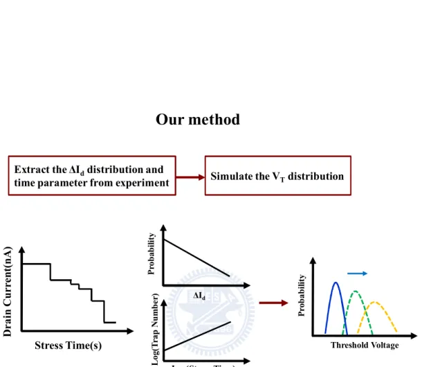
traditional method, we proposed a new method to simulate post-stress VT distribution
which showed in Fig. 2.2. In our method, the step-like drain current induced by single electron trapping is measured. According to ΔId probability distribution and the time
model, we can simulate the process of every single electron trapping. Finally the post-stress VT distribution is found.
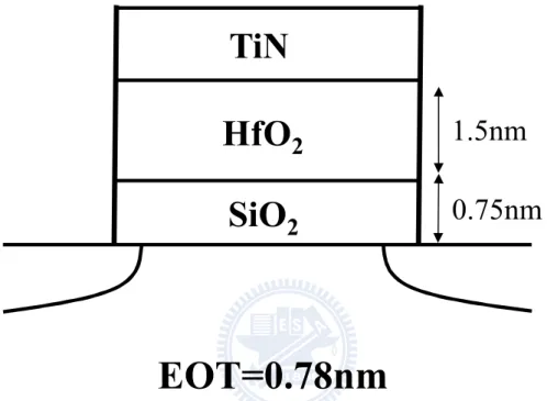
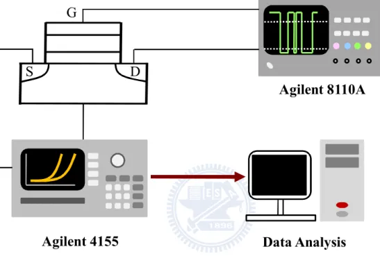
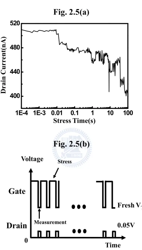
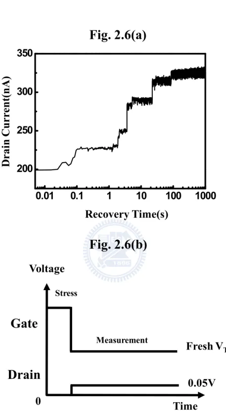
Fig. 2.3 showed the device structure in the following experiment, and the instrument setting is shown in Fig. 2.4. A two channel Agilent 8110 pulse generator connected to drain and gate electrode to simultaneously change the bias of each electrode, and the source electrode connected Agilent 4156 to measure the current. The trapped charge behavior in high-k dielectric is studied by “stress phase” and “recovery phase”, Fig. 2.5(a) and (b) illustrates a typical measurement result in stress phase, and the pulse pattern applied the gate and drain, respectively. A step-like drain current caused by single electron trapping is measured [2.2]. Similarly, the measurement result in recovery phase, and the pulse pattern applied are shown in Fig. 2.6(a) and (b). During the recovery phase, the phenomenon of trapped electrons discharge is observed [2.3-2.4]. The fast transient measure technique is proposed to minimize the switching delay time between stress and measurement, reduced the
6
amount of charge de-trapping in the delay time.
2.3 ΔI
dDistribution of PBTI
2.3.1 The Probability Function of ΔId in Recovery Phase
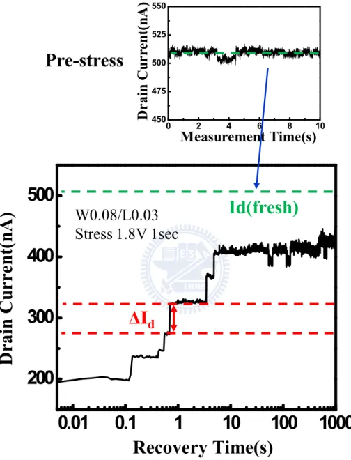
After a PBTI stress (1.8V 1sec), the recovery Id exhibits a step-like evolution in a
small device (W/L=0.08μm /0.03μm), and the ΔId amplitude is extracted as shown in
Fig. 2.7, we defined theΔId amplitude as following Eq. (2.1):
Eq. (2.1)
In order to have an equitable standard of the statistic, the current fluctuation ΔId is
normalized with Id (Fresh) which measured before the device being stress.
According to the result illustrated in Fig. 2.8, the probability distribution exhibited an exponential function, which showed that the amplitude of the drain current recovery induced by single electron de-trapping obeyed percolation theory. An empirical formula had been studied as following [2.5]:
Eq. (2.2a)
For convenience to observe the characteristic of the probability distribution, Fig. 2.8 is plotted in cumulative. In this case, Eq. (2.2a) should be integrated, Eq. (2.2b) showed the cumulative probability Function:
Eq. (2.2b) 100% ( ) (%) d d I I fresh Id amplitude
1exp d d I f I
exp d d I f I
7
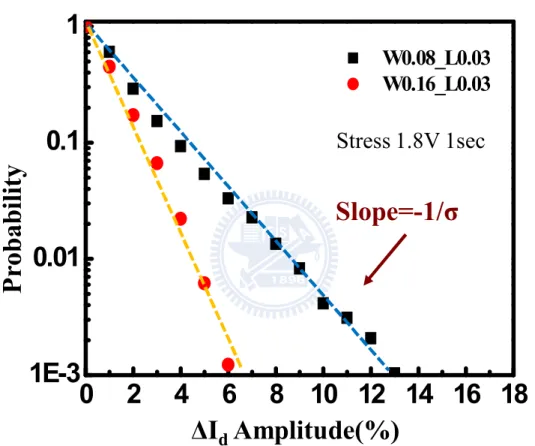
As the result of Eq. (2.2b), the slope of distribution showed in Fig.2.8 is -1/σ, a larger σ denoted the average ΔId induced by single electron is larger. From Fig. 2.7,
we compared the devices with two different dimensions (W0.08μm/0.16μm L0.03μm), a dimensional dependence of σ is investigated, which a larger device demonstrated a smaller σ [2.5], this phenomenon also followed the percolation theory.
When the device area is large the dopant can regard as uniform distributed in the substrate, as the device scaled down, the random dopant induced surface potential non-uniformity caused a current-path percolation, which called the percolation theory [2.6]. Compared the two figures of Fig. 2.9(a) and (b), an occupied interface trap is located on a critical path in Fig. 2.9(a), which induced larger current fluctuation than the Fig. 2.9(b) one.
2.3.2 Comparison of the ΔId Distribution in Different Condition
Based on the same method in recovery phase, we extracted the ΔId amplitude in
stress phase (stress1.3V 100sec), which illustrated in Fig. 2.10(a). Consequently, as the result showed in Fig. 2.10(b), ΔId distribution is consistent in stress and recovery
phase, which implied it followed the same mechanism in these two phase.
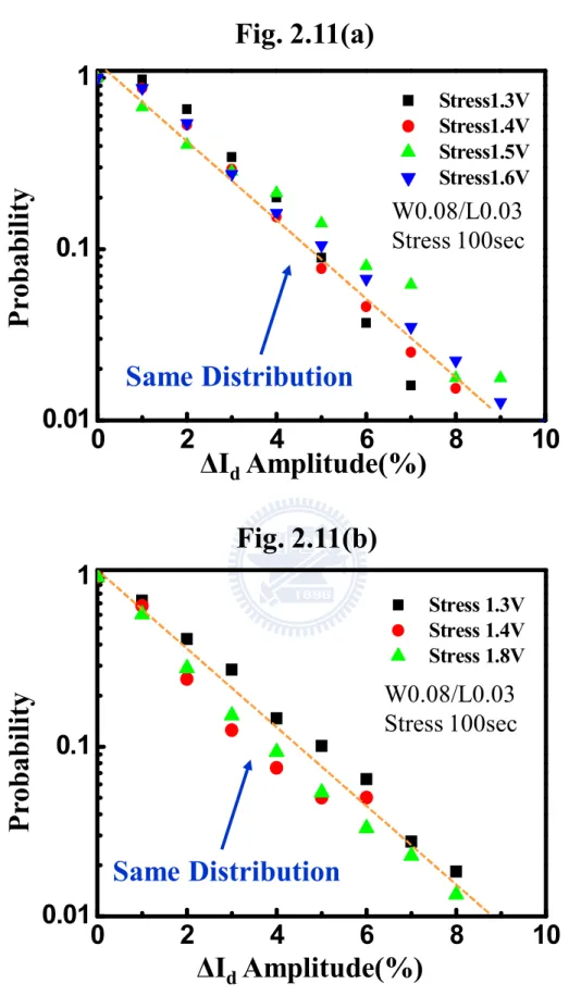
In this section, we compared the ΔId distribution in different stress voltage, Fig.
2.11(a) and (b) displayed the comparison of different stress voltage in stress and recovery phase respectively. ΔId distribution exhibited independent with stress voltage
neither in the stress and recovery phase.
2.3.4 The Difference of ΔId Distribution between Initial Trap and Stress Induced
8
In previous section, we discussed the ΔId distribution with different stress voltage
in stress and recovery phase. Currently, we compared the difference between initial trap and trap induced by PBTI stress. First, the ΔId distribution of RTN in a fresh
device and the PBTI ΔId distribution are illustrated in Fig. 2.12(a), from Table. 2.1 the
σ of PBTI is two times bigger than RTN in fresh device. Due to this phenomenon, we proposed an assumption. According to Fig. 2.12(b), on the random dopant region the surface potential is lower, which means the electron density is lower in this region. On the other hand, the electron density of the critical current path region is higher, it caused a higher probability of trap generation on the critical current path region. Hence, most of the stress induced trap located on the critical current path, it makes the σ of PBTI larger.
In Fig. 2.12(a), we also showed an evidence to support our assumption, the ΔId
distribution of post-stress RTN is similar to the PBTI one, and demonstrated a larger σ compared with the fresh one. As the result, the reliability problem of the stress induced trap is more serious than the initial trap.
2.4 The Time Model in Stress and Recovery Phase
2.4.1 The Time Model in Stress PhaseVT degradation can be measured in stress phase by the fast transient
measurement. Average each step-like data, as shown in Fig. 2.13 the threshold voltage shift versus stress time follows a perfect time-power law of the form [2.7-2.9]:
Eq. (2.3a)
nT
V t
t
9
Eq. (2.3b)
Fig. 2.14 showed that parameter n~0.232 in Eq. (2.3b) is consistent in different stress voltage.
Since the trap density has a power-law relationship with time, and the number of electron trapped should be proportional to trap density, we record the time of each electron trapped as illustrated in Fig. 2.15(a). We found that the number of electron trapped followed the same roles with time as in Eq. (2.4):
Eq. (2.4)
Fig. 2.15(b) showed that the time dependence with number of electron trapped can be well explained by Eq. (2.4).
2.4.2 The Time Model in Recovery Phase
There are three possible paths for electron de-trapping as illustrated in the energy band diagram in Fig. 2.16, i.e. Frenkel-Poole (F-P) emission, thermally assisted tunneling (TAT) to gate electrode, and TAT to substrate [2.4]. Using the Arrhenius equation in Eq. (2.5):
Eq. (2.5)
The extracted activation energy (Ea) is only 0.52eV as the result showed in Fig. 2.17.
The tunneling path is ruled out, since the activation energy for F-P tunneling should
log VT nlog t
log N nlog( )t
ln 1 a d E R d T 10
be equal to the trap energy (ET), which is over 1eV. According to the electron
emission time is proportional to the gate voltage, the tunneling path of TAT to gate can be excluded. TAT to substrate is the only reasonable explanation of the electron emission mechanism. Consequently, an analytical model of SRH-like thermally assisted tunneling is developed [2.4].
The analytical model of the tunneling mechanism can be displayed by the energy band diagram and trap distance in Fig. 2.18 [2.3-2.4]:
Eq. (2.6)
where
Eq. (2.6a)
Eq. (2.6b)
Eq. (2.6) reveals the nature of tunneling for trapped electron emission time, τi. The
pre-factor υ, a lumped parameter referred to as the ”attempt-to-escape frequency” can be written as Eq. (2.6a), where NC is the effective density-of-state in the Si conduction
ban, NC(1-fc) is the amount of available states in substrate for out-tunneling electrons
from high-k traps, σ0 and Ea are the cross-section and the activation energy.
According to the traps in the high-k layer can be recognized as a uniform distribution, the emission number increased with logarithmic time dependence as shown in Fig. 2.19.
1exp
exp
ox oxT
kx
1
0exp a c c th E N f kT
* 2 2 ox t B ox m q E * 2 2 k t k m qE 11
2.5 Width Dependence in PBTI Recovery
In the previous result, the larger device exhibited a smaller σ, but as a result of Eq. (2.6), it showed that as the cross section of the device increased, the more electrons had de-trapping in the same recovery time, which showed in Table. 2.2. According to Fig. 2.20, the analytical model of electron de-trapping is available in different dimension of device.
12
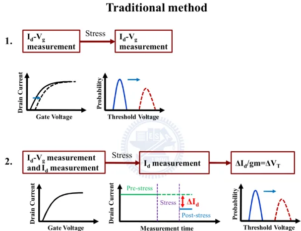
Fig. 2.1 Traditional method needs long measurement time and wastes lots of devices. .
Traditional method
Id-Vg measurement Stress Id-Vg measurement1.
Id-Vgmeasurement and Idmeasurement Stress Idmeasurement ΔId/gm=ΔVT2.
Threshold Voltage P ro b a b il it y Gate Voltage D ra in C u rr en t D ra in C u rr e n t Pre-stress Post-stress Measurement time Stress ΔId D ra in C u rr e n tGate Voltage Threshold Voltage
P ro b a b il it y
13
Fig. 2.2 Our method is based on characterizing the single charge phenomena, in order to simulate single electron trapped in PBTI.
Extract the ΔIddistribution and time parameter from experiment
Our method
Simulate the VTdistribution
P ro b a b il it y ΔId Threshold Voltage P ro b a b il it y D ra in C u rr en t( n A ) Stress Time(s) Log(Stress Time) L o g (T ra p N u m b e r)
14
Fig. 2.3 The high-k/metal gate device structure used in the following experiment.
TiN
HfO
2
SiO
2
1.5nm
0.75nm
EOT=0.78nm
15
Fig. 2.4 The instrument setting in order to achieve the fast transient measurement.
Agilent 4155
Agilent 8110A
Data Analysis
S
D
16
Fig. 2.5 (a) A typical pattern of Id degrade in PBTI stress phase, which cause by single
electron trapping.(b)Schematic of the constant voltage stress procedures.
1E-4 1E-3 0.01
0.1
1
10
100
400
440
480
520
D
ra
in
C
urr
ent(
nA
)
Stress Time(s)
Time
Fresh V
T StressVoltage
0.05V
MeasurementGate
Drain
0
Fig. 2.5(a)
Fig. 2.5(b)
17
Fig. 2.6 (a) A typical pattern of Id recovery in PBTI recovery phase, which cause by
single electron de-trapping.(b)Waveforms applied to gate and drain during stress and measurement.
0.01
0.1
1
10
100
1000
200
250
300
350
0
Time
0.05V
Gate
Drain
Measurement StressFresh V
TVoltage
Recovery Time(s)
D
ra
in
C
urr
ent(
nA
)
Fig. 2.6(a)
Fig. 2.6(b)
18
Fig. 2.7 To extract ΔId amplitude, we normalized ΔId with Id(fresh) for the same
criterion.
0.01
0.1
1
10
100
1000
200
300
400
500
0 2 4 6 8 10 450 475 500 525 550ΔI
dD
ra
in
C
u
rr
en
t(
n
A
)
Recovery Time(s)
Id(fresh)
W0.08/L0.03
Stress 1.8V 1sec
D
r
ai
n
C
u
r
re
n
t(
n
A
)
Measurement Time(s)
Pre-stress
19
Fig. 2.8 The ΔId amplitude follows exponential distribution caused by percolation
effect.
0
2
4
6
8 10 12 14 16 18
1E-3
0.01
0.1
1
W0.08_L0.03
W0.16_L0.03
P
ro
b
a
b
il
ity
ΔI
dAmplitude(%)
Stress 1.8V 1sec
Slope=-1/σ
20
Fig. 2.9(a) A interface trap located at critical path would make ΔId larger.(b) A
interface trap located at a insignificant point make smaller ΔId.
Random Dopant
Interface Trap Occupied by Electron Empty Interface Trap
Current Path Fig. 2.9(b)
21
Fig. 2.10 (a) Similarly, ΔId amplitude in stress phase is extracted.(b) The ΔId
distribution followed the same mechanism in stress and recovery phase.
1E-4 1E-3 0.01
0.1
1
10
100
360
400
440
480
520
0
2
4
6
8
10
12
14
1E-3
0.01
0.1
1
Stress Phase
Recovery Phase
P
ro
b
a
b
il
ity
ΔI
dAmplitude(%)
D
ra
in
C
u
rr
en
t(n
A
)
Stress Time(s)
ΔI
dFig 2.10(a)
Fig 2.10(b)
W0.08/L0.03
Stress 1.3V 100sec
22
Fig. 2.11 The ΔId distribution had no stress voltage dependence in (a) stress and (b)
recovery phase.
0
2
4
6
8
10
0.01
0.1
1
Stress 1.3V Stress 1.4V Stress 1.8V0
2
4
6
8
10
0.01
0.1
1
Stress1.3V Stress1.4V Stress1.5V Stress1.6VP
ro
b
a
b
il
ity
ΔI
dAmplitude(%)
Same Distribution
W0.08/L0.03
Stress 100sec
P
ro
b
a
b
il
ity
ΔI
dAmplitude(%)
W0.08/L0.03
Stress 100sec
Same Distribution
Fig. 2.11(a)
Fig. 2.11(b)
23
Table. 2.1 The stress induced trap exhibited a larger σ.
σ
PBTI
1.846
RTN
0.724
24
Fig. 2.12(a) The ΔId distribution of PBTI and post-stress RTN exhibited larger σ,
which means the stress induced traps located on the critical current path.
(b) The higher probability of trap generation on the high electron density region.
High electron density region
N
-aLow electron density region
0
2
4
6
8 10 12 14 16 18
1E-4
1E-3
0.01
0.1
1
Fresh RTN
PBTI
Post-stress RTN
P
ro
b
a
b
il
ity
ΔI
dAmplitude(%)
W0.08/L0.03
Stress 1.8V 1sec
Fig. 2.12(a)
Fig. 2.12(b)
25
Fig. 2.13 Threshold voltage shift versus stress time followed power-law of a device stressed under high gate voltage.
1E-4 1E-3 0.01
0.1
1
10
100
0
5
10
15
Device #1
Device #2
Average
Stress Time(s)
Δ
V
T(m
V
)
W0.08/L0.03
Stress 1.3V 100sec
26
Fig. 2.14 The ΔVT versus stress time characteristics under three different stress
voltage.
10
-61x10
-410
-210
010
20.01
0.1
1
10
100
Stress 1.3V
Stress 1.5V
Stress 1.6V
W0.08/L0.03
Stress 100sec
n≈0.232
Stress Time(s)
Δ
V
T(m
V
)
27
Fig. 2.15(a) We record the time of each electron trapped in the stress phase.
(b) The number of electron trapped versus stress time followed the same power-law.
1E-4 1E-3 0.01
0.1
1
10
100
400
440
480
520
Stress Time(s)
D
ra
in
C
u
rr
en
t(n
A
)
W0.08/L0.03
Stress 1.3V 100sec
0.01
1
100
0.1
1
10
Experiment Fitting resultW0.08/L0.03
Stress 1.3V 100sec
T
ra
p
N
u
m
b
er
Stress Time(s)
n≈0.232
log
N
n
log( )
t
Fig. 2.15(a)
Fig. 2.15(b)
28
Fig. 2.16 Energy band diagram illustrating possible paths for trapped charge emission.
TAT to
substrate
F-P emission
TAT to gate
29
Fig. 2.17 Temperature dependence of emission time.
3.0
3.1
3.2
3.3
3.4
0.01
0.1
1
Em
is
si
o
n
T
im
e
(s
)
1000/T
Slope=5.996
30
Fig. 2.18 Schematic representation of gate dielectric band diagram in recovery phase and trap positions, and the proposed model is described in detail in the text.
E
FT
oxE
TΦ
BTAT
x
31
Fig. 2.19 The emission number with a logarithmic time dependence during recovery.
1
2
3
4
5
6
1
10
100
log
e
Number
Number of τ
eEm
is
si
o
n
T
im
e(s
)
32
Fig. 2.20 NMOS recovery ΔVT traces in different dimensional device.
1E-3 0.01 0.1
0
1
10
100 1000
10
20
30
W0.03_L0.03
W0.08_L0.03
W0.16_L0.03
Recovery Time(s)
Δ
V
T(m
V
)
Stress 1.8V 1sec
33
Table. 2.2 A smaller device exhibited a larger σ, but when the cross-section increased more electrons are trapped in the same stress time.
34
Chapter 3
Monte Carlo Simulation of V
TDistribution in
PBTI Stress
3.1 Introduction
Using the result of the ΔId distribution and the time model respectively in stress
and recovery phase, we can simulate the VT shift after each electron trapped or
emission. Furthermore, the post-stress VT distribution can also be predicted by our
method, which is we can’t obtain from the traditional method. Finally, the divination of device lifetime is displayed, moreover, the VT distribution at lifetime is
investigated.
3.2 Simulation Flow
The model of single electron trapping/de-trapping is constructed in chapter 2. In this section, the procedure of Monte Carlo is introduced. Fig. 3.1 displayed the flow chart of the simulation.
First, as the result showed in Fig. 3.2, the fresh threshold voltage distribution can be finely approach with a Gaussian distribution Eq. (3.1):
Eq. (3.1)
Second, from the ΔId distribution extracted in the experiment, we applied a random
number y into the probability function to obtain the ΔId for each sample, moreover,
integrated with the time model, the VT degradation behavior in PBTI stress can be
2 2 1 ; , exp 2 2 x f x
35
simulated, as shown in Fig. 3.3(a) and (b) [3.1], respectively. Third, as the result in the last step, every sample had the correspondent ΔVT. Repeat the second and third step,
we can obtain the post-stress VT distribution, and the VT distribution after recovery is
simulated in a similar way. Fig. 3.4 illustrated the final result of the VT distribution of
the devices (W/L=0.08μm/0.03μm) under a PBTI stress (1.8V 1sec), and after 1000sec recovery.
3.3 Simulation of Width Dependence in PBTI Stress
Since the ΔId distribution is extracted in previous chapter, as the result in Table.
3.1, the smallest device (W/L=0.03μm/0.03μm) exhibited a largest σ in these three different dimension devices, which means a single electron trapped in these devices induced more VT shift. On the other hand, the σ of the largest device
(W/L=0.016μm/0.03μm) is smallest, but there are more electrons trapped in the same stress time due to the larger cross-section of the device. Fig. 3.5 demonstrated the simulation result of these three different dimension devices under the 1.8V 1sec PBTI stress. According to the result showed in Table. 3.1, VT shift is larger in the largest
device, which means not only the σ but also the number of trapped electrons effected the amount VT shift.
3.4 Simulation of Device Lifetime in PBTI Stress
Generally, we defined the device lifetime as the stress time that made the average VT shifted 0.1V, Fig. 3.6 illustrated how do we estimated the device lifetime in the
36
simulated, we proposed a new method to evaluate the device lifetime under a PBTI stress.
As shown in Fig.3.7 we can simulated the number of electron trapped that made the average threshold voltage shifted 0.1V. Consequently, the lifetime is calculated from the time model in the previous chapter. According to the experiment result, the ΔId distribution is consistent in the different PBTI stress voltage, we can derive the
conclusion that the post-stress VT distribution is the same at the device lifetime. Fig.
3.8 showed the corresponding VT distribution with an average threshold voltage
shifted 0.1V. Finally, we can predict the stress time which made the device reached a respective VT variation from the time model of each stress voltage Eq. (3.2).
Eq. (3.2)
As the result of Fig. 3.9, our method can perfectly estimate the device lifetime.
In the previous simulation we figure out the average device lifetime, although the average device lifetime exceed the 10 years line, there still have some devices couldn’t bare with the stress condition, the following theme discussed about the lifetime distribution of every devices. First, we simulate how many electrons should be filled that makes each sample across the deadline (post stress VT=0.464) as shown
in Fig. 3.10, and Fig. 3.11(a) demonstrated the probability distribution of the number
n
37
of jumps needed in every samples, as the previous result the ΔId distribution is the
same in different stress voltage, which means the probability distribution showed in Fig. 3.11(a) must be consistent in different stress voltage. Second, the number of jumps can be transformed to the device lifetime from the time model Eq. 3.2, the device lifetime distribution in stress voltage is shown in Fig. 3.11(b). Finally, the failure rate of the device in PBTI stress can be estimated, Fig. 3.12 demonstrated that in the stress voltage 1V condition, although the average device lifetime exceed the 10 years line, but there still have 9% devices failed.
38
Fig. 3.1 Flow chart of Monte Carlo simulation for post-stress VT distribution. 1.Use Gaussian distribution to
approach fresh VTdistribution
2. Use y=exp(-x/σ) to get the correspondent x(ΔId)
3.New VT1=Previous VT1+ΔVT1 New VT2=Previous VT2+ΔVT2 …and so on
4.The final VTdistribution
1. 2. 4. Threshold Voltage S a m p le N u m b er 3. Threshold Voltage S a m p le N u m b er Threshold Voltage S a m p le N u m b er ΔId P ro b a b il it y |Δ Id | Stress Time
39
Fig. 3.2 Gaussian distribution approach is appropriate in this simulation. .
0.25
0.30
0.35
0.40
0.45
0.00
0.02
0.04
0.06
0.08
0.10
0.12
0.14
Threshold Voltage(V)
Pr
o
b
a
b
il
it
y
40
Fig. 3.3 (a) A random number y is applied to obtain the corresponding ΔId according
to the ΔId distribution.(b) Using σ and the time model extract from experiment, we
can simulate the step-like VT variation.
0
40
80
120
1E-4
1E-3
0.01
0.1
1
y
exp
x
y
P
ro
b
a
b
il
ity
ΔI
d(nA)
10
-210
-110
010
110
20
5
10
15
20
25
Stress Time(s)
|Δ
V
T|(m
V
)
Fig. 3.3(a)
Fig. 3.3(b)
41
Fig. 3.4 The simulation of VT distribution under a PBTI stress (1.8V 1sec) and after
1000sec recovery.
0.3
0.4
0.5
0
2000
4000
6000
8000
10000
Fresh
After stress
After recovery
S
a
m
p
le
Nu
m
b
er
Threshold Voltage(V)
W0.08/L0.03 Stress 1.8V 1sec
Recovery 1000sec
42
Fig. 3.5 Due to the result, larger device exhibits more threshold shift under the same stress condition, which because more electrons trapped.
0.25 0.30 0.35 0.40 0.45 0.50 0.55
0
2000
4000
6000
8000
10000
Fresh
W0.03
W0.08
W0.16
S
a
m
p
le
Nu
m
b
er
Stress 1.8V 1sec
Threshold Voltage(V)
43
Table. 3.1 As the result, the variation of threshold voltage is concerned not only the σ but also the number of trapped electron.
Width
Average V
T(V)
σ
Number of
trapped
electron
0.03μm
0.38537
1.963
16
0.08μm
0.38765
1.846
20
0.16μm
0.39292
1.411
33
44
Fig. 3.6 The traditional method to estimate the device lifetime.
Traditional Method:
10
-610
-310
010
310
610
90.01
0.1
1
10
100
Stress 1.3V
Stress 1.5V
Stress 1.6V
Life Time
W0.08/L0.03
Stress Time(s)
Δ
V
T(m
V
)
45
Fig. 3.7 Evaluate the device lifetime due to the simulation of post-stress threshold voltage distribution.
Our Method:
Threshold Voltage S am p le N u m b er 0.1V VTshift Log(Stress Time) L og( T rap N u m b er ) N defects46
Fig. 3.8 According to the ΔId distribution is irrelevant to stress voltage, the post-stress
VT distribution is consistent due to the same VT variation.
0.3
0.4
0.5
0.6
0
5000
10000
15000
20000
Fresh 0.05V VT shift 0.1V VT shiftS
a
m
p
le
N
u
m
b
er
Threshold Voltage(V)
0 2 4 6 8 10 0.01 0.1 1 Stress1.3V Stress1.4V Stress1.5V Stress1.6VP
ro
b
a
b
il
ity
ΔI
dAmplitude(%)
Stress Phase
Same
Distribution
47
Fig. 3.9 As the result the device lifetime can perfectly estimate.
0.0
0.5
1.0
1.5
2.0
10
010
310
610
9Stress Voltage(V)
Li
fe
T
im
e(
s)
10 years
Experiment
Simulation
48
Fig. 3.10 The number of filled electron to make VT across deadline (0.464V) is different.
1E-6
1E-4
0.01
1
100
0.42
0.44
0.46
Deadline
28jumps 19jumps 20jumps Stress Time(s) T h re sh o ld V o lt a g e( V )49
Fig. 3.11(a) The probability distribution of the trap number. (b) The lifetime distribution transformed from (a).
10
-310
-110
110
310
510
70.000
0.004
0.008
0.012
0.016
Stress 1.6V Stress 1.5V10
100
0.000
0.004
0.008
0.012
0.016
Trap number
P
ro
b
a
b
il
ity
Lifetime(s)
P
ro
b
a
b
il
ity
Fig. 3.11(a)
Fig. 3.11(b)
50
Fig. 3.12 From the lifetime distribution we can estimate the failure rate of the samples under the PBTI stress.
0.0 0.5 1.0 1.5 2.0 102 104 106 108 1010 1012 0.000 0.004 0.008 0.012 0.016 102 104 106 108 1010 1012 Stress Voltage(V) L if e T im e (s ) 10 years L if et im e( s) Probability 9% Samples Failed Experiment Simulation
51
Chapter 4
Conclusion
Single Electron Phenomena in PBTI is characterizing in this work. We investigated the ΔId amplitude distribution followed the same mechanism in stress and recovery
phase, which is irrelevant to the stress voltage. Consequently, the ΔId distribution of
initial trap and stress induced trap is compared, as the result the stress induced trap caused more current fluctuation. On the other hand, based on the characterization in the stress and recovery phase, we derived the time model of PBTI. Also we observed that when device scales down, σ becomes larger but Id degradation cause by PBTI
stress is reduced, which because less traps.
According to the ΔId amplitude distribution and the time model obtained from
the experiment, a Monte Carlo simulation of VT distribution in PBTI is developed.
Due to the simulation we obtained the post-stress VT distribution, moreover, the
device lifetime can be estimated. Since the ΔId distribution is independent with the
stress voltage, VT distribution is the same at device lifetime in different stress
condition. The proposed method of simulate the post-stress VT distribution is a
52
Reference
Chapter 1
[1.1] J.H. Stathis, D.J. DiMaria, “Reliability projection for ultra-thin oxides at low voltage”, IEDM Tech. Dig.,1998 , pp. 167–170
[1.2] J. C. Lee, H. J. Cho, C.S. Kang, S.Rhee, Y.H.Kim, R.Choi, C. Y.Kang,C. Choi, M. Abkar, “High-k dielectrics and MOSFET characteristics”, IEDM Tech. Dig.,2003 , pp. 95-98
[1.3] A. S. Oates, “Reliability issues for high-k gate dielectrics”, IEDM Tech.
Dig.,2003 , pp. 923-926
[1.4] R. Degraeve, A. Kerber, P. Roussell, E.Cartier, T. Kauerauf, L. Pantisano, G. Groeseneken, “Effect of bulk trap density on HfO2 reliability and yield”, IEDM Tech.
Dig.,2003 , pp. 935-938
[1.5] S. Zafar, Y. H. Kim, V.Narayanan, C. Cabral Jr., V.Paruchure, B Dori, J. Stathis, A. Callerari, M. Chudzik, “A comparative study of NBTI and PBTI (Charge Trapping) in SiO2/HfO2 stacks with FUSI, TiN, Re Gates”, VLSI Tech. Dif., 2006, pp.23-25 [1.6] A. E. Islam, H. Kufluoglu, D. Varghese, S. Mahapatra, M. A. Alam, “Recent issues in negative bias temperature instability: initial degradation, field dependence of interface trap generation, hole trapping effects, and relaxation”, Electron Devices,
IEEE Transactions on., 2007, pp2143-2154
[1.7] T. Grasser, B. Kaczer, W. Goes, H. Reisinger, Th. Aichinger, Ph. Hehenberger, P.-J. Wagner, F. Schanovsky, J. Franco, Ph. Roussel, M. Nelhiebel, “Recent advances in understanding the bias temperature instaiblity”, IEDM Tech. Dig.,2010 , pp. 4.4.1 [1.8] C. T. Chan, C. J. Tang, T. Wang, C.-H. Wang, D.Tang, “Characteristics and physical mechanisms of positive bias and temperature stress-induced drain current degradation in HfSiON n MOSFETs” , Electron Devices, IEEE Transactions on.,
53
2006, pp.1340
[1.9] T. Wang, C. T. Chan, C. J. Tang, C.-H. Wang, C. W. Tsai, C.-H Wang, M. H. Chi, D.Tang, “A novel transient characterization technique to investigate trap properties in HfSiON gate dielectric MOSFETs-from single electron emission to PBTI recovery transient” , Electron Devices, IEEE Transactions on., 2006, pp.1073
Chapter 2
[2.1] K. Torii, K. Shiraishi, S. Miyazaki, K. Yamabe, M. Boero, T. Chikyow, K. Yamada, H. Kitajima, T. Arikado, “Physical model of BTI, TDDB and SILC in HfO2-based high-k gate dielectrics,” in IEDM Tech. Dig., 2004, pp. 129.
[2.2] K. Torii, K. Shiraishi, S. Miyazaki, K. Yamabe, M. Boero, T. Chikyow, K. Yamada, H. Kitajima, T. Arikado, “Positive bias temperature instability effects in nMOSFETs with HfO2/TiN gate stacks,” in Device and Materials.Reliability,
IEEE Transaction on, 2009, pp. 128.
[2.3] C. T. Chan, C. J. Tang, T. Wang, C.-H. Wang, D.Tang, “Characteristics and physical mechanisms of positive bias and temperature stress-induced drain current degradation in HfSiON n MOSFETs” , Electron Devices, IEEE Transactions on.,
2006, pp.1340
[2.4] T. Wang, C. T. Chan, C. J. Tang, C.-H. Wang, C. W. Tsai, C.-H Wang, M. H. Chi, D.Tang, “A novel transient characterization technique to investigate trap properties in HfSiON gate dielectric MOSFETs-from single electron emission to PBTI recovery transient” , Electron Devices, IEEE Transactions on., 2006, pp.1073 [2.5] A. Ghetti et al, IEDM, p.835, 2008
[2.6] Koichi Fukuda, Yuui Shimizu, Kazumi Amemiya, Masahiro Kamoshida, Chenming Hu, “Random telegraph noise in flash memories-model and technology scaling” in IEDM Tech. Dig., 2007, pp. 169.
54
[2.7] M.A. Alam, S. Mahapatra, “A comprehensive model of PMOS NBTI degradation” in Microelectronics Reliability., 2005, pp. 71-81.
[2.8] N. Sa, J. F. Kang, H. Yang, X. Y. Liu, Y. D. He, R. Q. Han, C. Ren, H. Y. Yu, D. S. Chan, D.-L. Kwong, “Mechanism of positive-bias temperature instability in
sub-1-nm TaN/HfN/HfO2 gate stack with low preexisting traps” in Electron Device
Letters. , 2005, pp. 610.
[2.9] Moonju Cho, M. Aoulaiche, R. Degraeve, B. Kaczer, J. Franco, T. Kauerauf, “Positive and negative bias temperature instability on sub-nanometer eot high-k MOSFETs” in IRPS. , 2010, pp. 1095.
Chapter 3
[3.1] T. Grasser, B. Kaczer, W. Goes, H. Reisinger, Th. Aichinger, Ph. Hehenberger, P.-J. Wagner, F. Schanovsky, J. Franco, Ph. Roussel, M. Nelhiebel, “Recent advances in understanding the bias temperature instaiblity”, IEDM Tech. Dig.,2010 , pp. 4.4.1
55