487 Annealing Temperature Dependence of Electric Conduction
and Capacitance Dispersion in Nitrogen-Implanted GaAs
Journal of ELECTRONIC MATERIALS, Vol. 30, No. 5, 2001
(Received June 14, 2000; accepted January 8, 2001)
Regular Issue Paper
487 INTRODUCTION
Since nitrogen is a relatively light ion, high energy nitrogen implantation can produce a buried layer in GaAs. Because this highly-damaged layer is readily removable by defect-sensitive etchants, it can be used as a sacrificial layer for three-dimensional microstructuring.1,2 Also, since annealing after
nitro-gen implantation has been shown to produce highly resistive n-type GaAs,3 this buried layer can also be
used for electrical isolation. Recently, deep levels in nitrogen-implanted GaAs were studied.4 In addition,
a theoretical calculation predicts that the band gap of GaAs1-xNx decreases with increasing x,5 which has
been demonstrated experimentally.6–8 An emission at
around 1.3 eV9 was observed at 2 K after high-energy,
high-dose N implantation into GaAs. Despite these studies, little is known about the annealing behavior of the structural and electrical properties of nitrogen-implanted GaAs. Therefore, in this letter, we use current-voltage (I-V) and capacitance-frequency (C-F) spectroscopy to investigate the electrical proper-ties of nitrogen implanted GaAs films annealed at different temperatures.
Annealing Temperature Dependence of Electric
Conduction and Capacitance Dispersion in
Nitrogen-Implanted GaAs
J.F. CHEN, M.M. HUANG, and J.S. WANG
National Chiao Tung University, Department of Electrophysics, Hsinchu, Taiwan, R.O.C The annealing behavior of nitrogen-implanted GaAs samples has been investi-gated by secondary ion mass spectroscopy, current-voltage (I-V) and capaci-tance-frequency (C-F) measurements. The I-V data show that the conductivity of as-implanted samples is dominated by variable-range hopping between defect states below 300 K. The implanted layer becomes highly resistive after anneal-ing. The activation energy of the resistance is found to increase from 0.2 eV for as-implanted samples to 0.71 eV for 950°C-annealed samples. Significant capacitance dispersion is observed over frequency for implanted samples. Based on a proposed equivalent circuit, the high-frequency capacitance dispersion is shown to be the result of resistance-capacitance (RC) time constant effects. The increase of activation energy of the resistance can be explained by the creation of deep traps by high temperature annealing. Traps at 0.69 eV and 0.82 eV are detected for 700°C and 950°C-annealing, respectively.
Key words: Nitrogen implantation, annealing, capacitance-frequency spectroscopy, deep traps
EXPERIMENT
A nitrogen implantation at an energy of 160 keV with a dose of 2 × 1015 cm–2 was performed at room
temperature into (001) Si-doped liquid encapsulated Czochralski (LEC) n+-GaAs substrates with a carrier
concentration on the order of 1018 cm–3 and into
semi-insulating GaAs substrates. The implanted samples were set face-to-face with GaAs wafers for annealing in an N2-flow furnace from 200°C to 700°C for 30 min.
For annealing temperatures higher than 700°C, rapid thermal annealing was used for 30 sec. Following annealing, ohmic contacts were made on the surface of the samples by alloying Au/Ge while 1000 µm diameter Schottky contacts were made by evapora-tion of Al.
MEASUREMENTS AND RESULTS Secondary Ion Mass
Spectroscopy Measurement
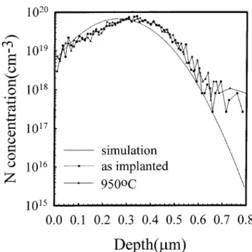
Figure 1 shows the secondary ion mass spectros-copy (SIMS) profiles of nitrogen in as-implanted and 950°C annealed n+-GaAs substrates. The N
concen-tration increases to a maximum at a depth of 0.34 µm and then falls below the background concentration at about 0.65 µm, beyond which the N concentration
deviates from the simulated profile. The profiles were found to be in general agreement with the simulated profile using transport of ions in matter (TRIM). The profiles display no significant difference between as-implanted and 950°C annealed samples, indicating no redistribution of N even after 950°C annealing. No pileup of N was observed at the surface.
Conduction of As-Implanted Sample
Because the highly conductive nature of the im-plant, Semi-insulating GaAs was used as the sub-strate to avoid the unwanted conduction from the
substrate. Figure 2 shows the ohmic I-V characteris-tics for the as-implanted sample. The current consists of two distinct regions: a linear low-voltage and an exponential high-voltage region. This conduction be-havior is similar to that of an n-i-n structure.10 It is
known that the current of the n-i-n structure at low voltage is due mainly to thermally generated carriers which constitute an ohmic current. Therefore, the inverse of the slope in the linear region was taken as the resistance and the results are shown as hollow circles in Fig. 3. The resistance is about 103Ω at room
temperature and its temperature dependence can be expressed as R = R0 exp(Ea/kT) for T > 300 K, where R0
is a constant, Ea is the activation energy and k is the
Boltzmann constant. From Fig. 3, Ea was determined
to be 0.2 eV. Similar activation energy of 0.1 eV was reported for As-implanted GaAs at T > 300 K.11
Below 300 K, the conductance Gs of the
as-im-planted sample as shown in the inset of Fig. 3, is found to be dominated by variable-range hopping12, that is, G
s
∝ exp(–β/T1/4) here β is a constant and was
experimen-tally estimated to be 62 K1/4. This value is close to 64 and
66 K1/4 for the as-grown LT-GaAs13 and non-annealed
As-implanted GaAs,14 respectively. This result
indi-cates that N implanted GaAs has a similar concentra-tion of defects as LT-GaAs and As-implanted GaAs, which contributes to the hopping conduction. From β = 2(3/2π)1/4[α3/kN (E
F)]1/4 = 62 K1/4 and α = (2m*Ea)1/2/ h,
where m* = 0.07 m
o is the effective mass of an electron
in GaAs, the density of states N(EF) was calculated to
be about 2 × 1018 cm–3 eV–1. According to Mott12 and
Shklovskii,15 conduction can occur by hopping through
defect states. Usually variable-range hopping is ob-served at very low temperature. However, it has been reported to occur even at room temperature.14 Fig. 1. The SIMS profiles of nitrogen in as-implanted and 950o
-annealed samples as well as the simulated profile using transport of ions in matter (TRIM) simulation.
Fig. 2. The temperature-dependent I-V characteristics of the as-implanted sample.
Fig. 3. The resistance of the as-implanted sample, obtained from the linear region of the I-V curves in Fig. 3, along with that from the capacitance-frequency (C-F) spectra. Shown in the inset is the tem-perature-dependent conductance of the as-implanted sample.
489 Annealing Temperature Dependence of Electric Conduction
and Capacitance Dispersion in Nitrogen-Implanted GaAs
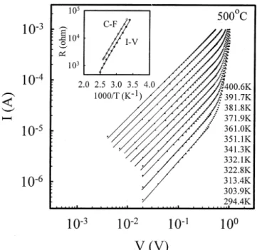
Conduction of 500°C-Annealing Sample
Annealing has the effect of reducing the conductiv-ity. Figure 4 shows the ohmic I-V characteristics for the 500°C-annealed sample. These I-V characteris-tics are similar to those of the as-implanted sample except the current is lower. Taking the inverse of the slope in the linear low-voltage region as the resistance of the implanted layer, the resistance is about 105Ω at
300 K, which is higher than that for as-implanted sample. This can be explained by the reduction of hopping conduction due to the decrease in the defect concentration. The activation energy of the resistance was determined to be 0.34 eV, as shown in the inset of Fig. 4, implying that the conduction is dominated by thermal excitation from defect states to the conduction band and the Fermi energy is pinned at this energy. Schottky I-V Characteristics
In order to study the deep traps, Schottky diode was made by evaporating Al on the front surface of the implanted sample while the ohmic contact was made by heating In to the back surface after the implanta-tion. The Schottky I-V characteristics at 300 K are shown in Fig. 5 for all samples. The as-implanted and 500°C-annealing samples display almost no rectify-ing effect because their I-V curves are nearly symmet-ric. Some rectifying effect can be seen for the 700°C and 950°C-annealed samples, especially for the 700°C case. Their forward current increases exponentially and then is suppressed at large bias as can be seen in semi-log scale (not shown here), similar to what is expected from a Schottky diode in series with a large resistance. At very small voltages, the forward cur-rent for the 950°C-annealed sample displays an addi-tional ohmic leakage component.
Capacitance-Frequency Measurement
Because of the difficulty of modulating a highly resistive layer, we use C-F measurements instead of deep-level transient spectroscopy (DLTS) to charac-terize the deep traps. The C-F measurement was performed using a HP4194A gain-phase analyzer with an oscillation level of 0.1 V. Figure 6 shows the temperature-dependent C-F spectra at V = –1 V for as-implanted, 500°C, 700°C, and 900°C-annealed samples. Significant capacitance dispersion over fre-quency was observed for each sample. The as-im-planted and 500°C-annealed samples show one step-like capacitance drops while the 700°C and 900° C-annealed samples show two step-like capacitance drops over frequency. In general, this capacitance dispersion is interpreted as a trapping effect from defect levels. However, the implanted sample pos-sesses a highly resistive layer which may introduce a resistance-capacitance (RC) time constant effect. We
Fig. 4. The temperature-dependent I-V characteristics of the 500o C-annealed sample. Shown in the inset is the resistance obtained from the linear region along with that obtained from the capacitance-frequency (C-F) spectra.
Fig. 5. The Schottky I-V characteristics at 300 K for substrate, as-implanted, 500°C, 700°C, and 950°C-annealed samples.
Fig. 6. The temperature-dependent C-F spectra at V = –1 V for as-implanted, 500°C, 700°C, and 950°C-annealed samples.
believe that the capacitance drops in as-implanted and 500°C samples and the high-frequency capaci-tance drops in 700°C and 950°C-annealing samples are due to this RC effect.
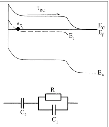
To show the RC effect, let us assume a single trap level in the implanted region to compensate the shal-low ionized donor (not shown) and produce a highly resistive layer. A simplified band diagram and its corresponding equivalent circuit are shown in Fig. 7. Upon applying an oscillating voltage, the traps at the crossing point of the trap level and Fermi level will emit electrons with an emission time, τt , and traverse
through the rest of the highly resistive layer with a time constant, τRC = R(C1 + C2), here R and C1
repre-sent the rest of the high-resistive layer and C2 is the
effective Schottky depletion capacitance. If τRC > τ1,
the observed time constant will be dominated by τRC.
Based on this equivalent circuit, the total equivalent capacitance is given by C C C C C C C R C C ( ) / ( ) ω ω = + + + + 1 2 1 2 2 1 2 2 1 2 2 1 1 (1)
Note that the total capacitance exhibits a step-like capacitance drop over frequency.
From Eq. 1, the inflection frequency at which C drops from high to low plateaus occurs at ω = τ–1 =
[R(C1 + C2)]–1. Let us roughly determine the inflection
frequency from the resistance estimated from the Schottky I-V characteristics in Fig. 5. Choosing the
large forward voltage of 3 V, the current is 3 × 10⁻³ A
for the as-implanted sample, giving an R =103 Ω.
Similarly, I = 4.3 × 10⁻⁵ A for both 500°C and 950°
C-annealed samples, yielding an R = 7 × 10⁴Ω, and I =
3 × 10⁻⁵ A for 700°C-annealed sample, yielding an R =
105Ω. From these R, in conjunction with C
1 and C2 in
Fig. 6, the inflection frequencies were estimated to be 2.6 × 10⁴, 284 Hz, 3183 Hz, and 1137 Hz, as indicated
by the arrows in Fig. 6, for as-implanted and 500°C, 700°C, and 950°C-annealed samples. These values are close to the experimental inflection frequencies (at 300 K). This result suggests that the C drops in as-implanted and 500°C samples and the high-frequency C drops in 700°C and 950°C-annealing samples are due to the effects of RC time constants.
Since the inflection frequency reflects the RC time constant. We can convert the inflection frequencies at different temperatures to obtain the activation ener-gies of R and their results are shown in Fig. 3 for as-implanted and in the inset of Fig. 4 for 500° C-annealed samples. Comparing with the resistance obtained from I-V characteristics, it can be seen that the resistance obtained from C-F spectra are in agree-ment with those from the I-V data for both cases. This further confirms the RC time constant effects. Figure 8 shows the values of the resistance R con-verted from the RC time constants in C-F spectra. The activation energies are 0.20 eV, 0.34 eV, 0.59 eV, and 0.71 eV for as-implant, 500°C, 700°C, and 950° C-annealing samples. This result indicates that the Fermi energy is pinned toward the midgap as the annealing temperature increases.
At high frequencies, where the carriers emitted from the traps cannot follow the frequency to traverse through the high-resistive layer, that is, 1/ω << (C1 +
C2)R, Eq. 1 reduces to Ch = C1C2/(C1 + C2) which
corresponds to the total thickness of the high-restive
Fig. 7. The simplified band diagram showing a single trap level in the implanted region and its corresponding equivalent circuit. The C2 represents the effective Schottky depletion layer while R and C1 represent the rest of the highly resistive layer.
Fig. 8. The resistance R derived from the RC time constants in C-F spectra.
491 Annealing Temperature Dependence of Electric Conduction
and Capacitance Dispersion in Nitrogen-Implanted GaAs
layer and the effective Schottky depletion width. The experimental Ch is virtually independent of voltage
for all four samples. Figure 6 shows that Ch are 1400 pF,
300 pF, 359 pF, and 270 pF for as-implanted, 500°C, 700°C, and 950°C-annealed samples, corresponding to 0.15 µm, 0.68 µm, 0.57 µm, and 0.76 µm. Neglecting the modification of the effective Schottky depletion width, the thickness obtained for as-implanted sample is much smaller than the effective implanted thick-ness of 0.65 µm estimated from SIMS profile. We spec-ulate that an amorphous structure exists in the surface due to the ion damage. An amorphous structure has been reported in the surface of arsenic-implanted GaAs.16 For annealed samples, the obtained
thick-ness is close to 0.65 µm, suggesting that, after anneal-ing, almost all of the portion of the implanted region with the N concentration higher than the background concentration becomes highly resistive.
At low frequencies where 1/ω >> R(Cd + Cr), Eq. 1
reduces to the effective Schottky capacitance C2. From
values of C2 in Fig. 6, we obtained the effective
depletion widths of 0.037 µm, 0.03 µm, 0.39 µm, and 0.12 µm for as-implanted, 500°C, 700°C, and 950° C-annealed samples. Note that 700°C-annealed sample has the largest depletion width, which is consistent with the strongest rectifying I-V curve in Fig. 5. The small depletion widths for as-implanted and 500° C-annealed samples result in a poor rectification due to strong field emission. The depletion width obtained here is determined by the space charge NSC in the
Schottky depletion region. When an acceptor of con-centration NA is present, NSC = ND+ if it is unoccupied
or NSC = ND+ – NA− if it is occupied by electrons, where
ND+ is the shallow ionized donor whose magnitude is
on the order of 1018 cm–3. We assume that the carriers
in the 500°C-annealed sample are depleted by an acceptor level at 0.34 eV with a concentration large enough to pin the Fermi level. Due to the Schottky barrier effect, this acceptor level is probably above the Fermi level and is unoccupied in the Schottky deple-tion region. Let us estimate the Schottky depledeple-tion width using an abrupt junction approximation x = [2εS(Vbi + VR)/eNSC]1/2, where VR = 1V, Vbi = (0.9–0.34)V,
taking 0.9 eV as the Schottky barrier height. If we substitute NSC = ND+ = 2 × 10
18 cm–3 we obtain x =
0.03 µm. Consequently, an acceptor level at 0.34 eV and the shallow ionized donor alone could result in the observed depletion width for the 500°C-annealed sample. As for the large depletion widths in 700°C and 950°C-annealed samples, a reasonable speculation is that there exists another acceptor level in the Schottky depletion region, which is below the Fermi energy to compensate the shallow ionized donor. From their individual Fermi energies, this acceptor level should be deeper than 0.59 eV and 0.71 eV, respectively, for 700°C and 950°C-annealed samples.
Figure 6 shows that besides the high-frequency capacitance drop representing the RC time constant effect, other capacitance drops appear at high tem-perature and low frequency for the 700°C and 950° C-annealed samples. Since the emission times were
more than two order of magnitudes longer than the RC time constant, they would not be affected by the RC time constant if the carriers emit from the traps in the Schottky depletion region. From their Arrhenius plots, activation energies (capture cross sections) were determined to be 0.69 eV (2.4 × 10⁻¹² cm2) and 0.82 eV
(2.6 × 10⁻¹² cm2), respectively, for 700°C and 950°
C-annealed samples. Note that both traps are deeper than the Fermi energies (0.59 eV and 0.71 eV, respec-tively, for 700°C and 950°C-annealed samples), so they are capable of compensating the shallow ionized donor in the Schottky depletion region. The fact that these traps were not observed in as-implanted and 500°C-annealed samples suggests that they were introduced after high temperature annealing. The large activation energies for the resistance in 700°C and 950°C-annealing samples might be explained by the effect of these deeper levels. Significant modifica-tion of the electrical properties of a surface layer of implanted GaAs was found due to defect or impurity redistribution after thermal annealing at tempera-tures as high as 800~900°C.17 Comparing with other
reported traps, our traps at 0.69 eV and 0.82 eV are similar to EL18 (0.76 eV, 5 × 10–12 cm-2) and EL2
(0.825 eV, 1.2 × 10⁻¹³ cm–2), respectively.18 As for the
500°C-annealed sample, besides the possible exist-ence of the relatively shallow trap which contributes to the observed RC effect, Fig. 6 shows no other deep levels. This is consistent with the observed small Schottky depletion width. The low activation energy (0.34 eV) for its resistance also implies that carrier depletion is mainly due to relatively shallow traps.
CONCLUSIONS
We have studied the annealing temperature depen-dence of electrical properties of N implanted GaAs. It has been found that the N implantation can increase the sample’s resistance. Current conduction in as-implanted sample is dominated by variable-range hopping between defect states. After annealing, the resistance of implanted layer increases. The activa-tion energy of the resistance is found to increase with increasing annealing temperature. This may be at-tributed to the creation of deep levels by high tem-perature annealing. Detailed analysis of the C-F spectra revealed two traps at 0.69 eV and 0.82 eV, respectively, in 700°C and 950°C-annealed samples.
ACKNOWLEDGEMENT
The authors would like to thank Dr. N.C. Chen for many useful discussions and the National Science Council of the Republic of China for financially sup-porting this research under Contract No. NSC-87-2112-M-009-022.
REFERENCES
1. J. Miao, I.M. Tinginyanu, H.L. Hartnagel, G. Irmer, J. Monecke, and B.L. Weiss, Appl. Phys. Lett. 70, 847 (1997). 2. J. Wurfl, J. Miao, D. Ruck, and H. Hartnagel, J. Appl. Phys.
72, 2700 (1992).
3. W.M. Duncan, and S. Matteson J. Appl. Phys. 56, 1059 (1984).
4. K.M. Chen, Y.Q. Jia, Y. Chen, A.P. Li, S.X. Jin, and H.F. Liu,
J. Appl. Phys. 78, 4262 (1995).
5. S. Sakai, Y. Ueta, and Y. Terauchi, Jpn. J. Appl. Phys. 32, 4413 (1993).
6. M. Weyers, M. Sato, and H. Ando, Jpn. J. Appl. Phys., Part
2 31, L853 (1992).
7. M. Kondow, K. Uomi, K. Hosomi, and T. Mozume, Jpn. J.
Appl. Phys., Part 2 33, L1056 (1994).
8. K. Uesugi, N. Morooka, and I. Suemune, Appl. Phys. Lett. 74, 1254 (1999).
9. T. Shima, S. Kimura, T. Iida, A. Obara, Y. Makita, K. Kudo, and K. Tanaka, Nucl. Instr. and Meth. in Phys. Res. B 118, 743 (1996).
10. J.F. Chen, N.C. Chen, S.Y. Chiu, P.Y. Wang, W.I. Lee, and A. Chen, J. Appl. Phys. 79, 8488 (1996).
11. H. Fujioka, J. Krueger, A. Prasad, X. Liu, E.R. Weber, and A.K. Verma, J. Appl. Phys. 78, 1470 (1995).
12. N.F. Mott and W.D. Twose, Adv. Phys. 10, 107 (1961). 13. D.C. Look, Z.-Q. Fang, J.W. Look, and J.R. Sizelove, J.
Electrochem. Soc. 141, 747 (1994).
14. G.R. Lin, W.C. Chen, C.S. Chang, and C.L. Pan, Appl. Phys.
Lett. 65 3272 (1994).
15. B.I. Shkllovskii, Sov. Phys. Semicond. 6, 1053 (1973). 16. A. Claverie, F. Namaver, and Z. Liliental-Weber, Appl. Phys.
Lett. 62, 1271 (1993).
17. G.M. Martin, P. Secordel, and C. Venger, J. Appl. Phys. 53, 8706 (1982).
18. G.M. Martin, A. Mitonneau, and A. Mircea, Electron. Lett. 13, 191 (1977); and A. Mitonneau, G.M. Martim, and A. Mircea, Electron. Lett. 13, 666 (1977).