that without CF4plasma treatment. The maximum off-state leakage current of the fluorine-passivated TFT is more than one order of magnitude lower than that of the control TFT. Furthermore, the incorporation of fluorine atoms by CF4plasma treatment also improves the reliability of poly-Si Pr2O3TFTs against hot carrier stressing, which is due to the formation of stronger Si–F bonds in place of weak Si–H bonds in the poly-Si channel and at the Pr2O3gate dielectric/poly-Si interface. Therefore, high-performance and high-reliability poly-Si TFTs with Pr2O3gate dielectric and CF4plasma treatment on poly-Si film are suitable for active-matrix liquid crystal display application.
© 2007 The Electrochemical Society. 关DOI: 10.1149/1.2816281兴 All rights reserved.
Manuscript submitted August 22, 2007; revised manuscript received October 22, 2007. Available electronically December 6, 2007.
Polycrystalline silicon thin-film transistors共poly-Si TFTs兲 have received considerable attention in fields such as large-area electronic applications including linear image sensors and active-matrix liquid crystal displays 共AMLCDs兲.1,2 The major application of poly-Si TFTs in AMLCDs lies in integrating the peripheral driving circuits and the pixel switching elements on the same glass substrate to realize system-integration-on-panel technology.3 The complicated process can be greatly simplified and the fabrication cost can be reduced by realizing system-integration-on-panel technology. How-ever, it is difficult to develop high-performance and high-reliability poly-Si TFTs that are applicable for both pixel-switching elements and peripheral driving circuits. Pixel-switching elements require TFTs to operate at high voltages as well as low gate-leakage currents to drive the liquid crystal. In contrast, TFTs with good electrical characteristics, including low operation voltage, low subthreshold swing, high driving current, and low gate-leakage current, are nec-essary for achieving the peripheral driving circuit applications. Be-cause poly-Si TFTs are usually fabricated on inexpensive glass sub-strate, a low-temperature process is required for the realization of commercial flat-panel displays. The solid-phase crystallization 共SPC兲 process with a maximum process temperature limited to 600°C is widely used to recrystallize amorphous Si film due to its low production cost and good grain-size uniformity.4Poly-Si TFT with a thinner physical gate-dielectric thickness can increase the gate capacitance density and enhance the driving-current capability. However, a higher gate-leakage current could be introduced by the thinner gate dielectric, exhibiting significantly degraded electrical characteristics of poly-Si TFT.5
Several high- materials, including oxide/nitride/oxide 共ONO兲 gate stack, Al2O3, and Ta2O5, were proposed to replace
conven-tional SiO2to serve as the gate dielectrics of poly-Si TFTs.6-8The
gate capacitance density of high- gate dielectrics is higher than that of SiO2gate dielectric. To reach the same value of gate capacitance
density, the physical thickness of the high- gate dielectrics can be thicker than that of the SiO2gate dielectrics. Therefore,
incorporat-ing high- gate dielectrics into poly-Si TFTs could induce a higher mobile carrier density in the channel region and suppress the gate-leakage current to improve gate controllability. However, such high gate capacitance density would contribute to a high electric field at the gate-to-drain overlap area, resulting in a rather high field-enhanced emission via the trap states at the grain boundaries.
There-fore, poly-Si TFTs with high- gate dielectric would suffer from a more undesirable gate-induced drain leakage 共GIDL兲 current.9 To address this GIDL issue, various techniques, including hydrogen-plasma treatment and fluorine-ion implantation on poly-Si film, have been applied to effectively improve the device performance by re-ducing the trap state densities.10-13 However, the hydrogenated poly-Si TFTs suffer from an instability issue due to the easily broken weak Si–H bonds.11 In contrast, the fluorine-ion implantation on poly-Si film can improve the electrical stability of poly-Si TFTs due to the rather strong Si–F bond formation in the poly-Si channel and at the gate dielectric/poly-Si interface.12,13 Nevertheless, the ion-implantation method has troublesome problems in large-area elec-tronics, and high-temperature annealing is also required to activate implanted fluorine ions and cure implant damages.
Recently, praseodymium oxide共Pr2O3兲 has become a promising high- gate-dielectric candidate in metal-oxide-semiconductor field-effect transistors due to its high dielectric constant value of about 31, low gate-leakage current, good dielectric property, and superior thermal stability.14,15We have fabricated high-performance poly-Si TFTs using Pr2O3as gate dielectric in a recent study.16In this work, we report a fluorine-passivation technique without ion implantation and an additional annealing step by employing a low-temperature CF4plasma treatment. The fluorine atoms dissociated from the CF4 reaction gas can be introduced into the poly-Si film and then passi-vate the trap states at the grain boundaries. We have integrated a process-compatible fluorine-passivation technique and a high- Pr2O3gate dielectric into poly-Si TFTs and investigated their device
characteristics and reliability.
Experimental
Figure 1 illustrates the key fabrication steps for the proposed poly-Si Pr2O3TFTs with CF4plasma treatments. Briefly, the fabri-cation began by depositing a 100 mm undoped amorphous silicon 共␣-Si兲 layer on a thermally oxidized Si wafer using low-pressure chemical vapor deposition 共CVD兲 at 550°C. The deposited ␣-Si layer was then recrystallized by the SPC process at 600°C for 24 h in N2ambient. The individual active region was patterned and de-fined. After the RCA clean process, a CF4 plasma treatment was applied on the recrystallized poly-Si film by plasma-enhanced CVD 共PECVD兲 at 350°C 共Fig. 1a兲. The chamber pressure and flow rate of CF4reaction gas were 400 mTorr and 80 sccm, respectively. To in-vestigate the effect of fluorine content on the poly-Si Pr2O3 TFT, various radio frequency 共rf兲 powers of 0, 10, and 20 W, with a constant treating time of 20 s, were used to perform the CF4plasma z
treatment. Afterward, a 33.6 nm Pr2O3film was deposited to serve as the gate dielectric by electron-beam evaporation, followed by a realization of thermal annealing treatment at 600°C for 30 min in O2ambient to improve the gate-dielectric quality. After a 200 nm TiN film was deposited, a Cl2-based dry-etching process capable of
stopping on the Pr2O3layer was used to pattern the gate electrode.
After a self-aligned phosphorous ion implantation was performed at 80 keV to a dose of 5⫻ 1015cm−2to dope the source/drain regions,
the dopant was activated by the thermal budget of 600°C for 30 min 共Fig. 1b兲. After a 300 nm passivation SiO2layer was deposited by
PECVD at 300°C, the contact windows were opened by a two-step wet-etching process. First, the 300 nm passivation SiO2 layer and the Pr2O3layer were etched away by a buffered oxide etch solution and a H2SO4/H2O2mixture solution, respectively共Fig. 1c兲. Because the H2SO4/H2O2mixture solution has a rather high etch selectivity
of the Pr2O3thin film to the SiO2passivation layer, a Pr2O3film can
be completely etched away by excessive overetching. Finally, a typi-cal 400 nm Al metallization completed the fabrication process共Fig. 1d兲. For comparison, the control poly-Si Pr2O3TFT without the CF4
plasma treatment, rf power of 0 W, was also prepared with the same process flow. No hydrogen plasma treatment and thermal sintering process were performed to study the fluorine-passivation effects.
Results and Discussion
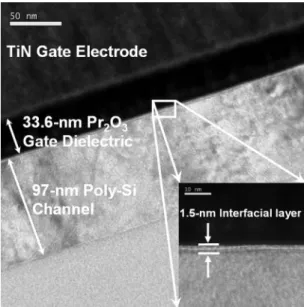
Figure 2 shows the cross-sectional transmission electron micros-copy共XTEM兲 micrograph of the proposed poly-Si TFT with TiN gate electrode and Pr2O3gate dielectric on the poly-Si channel. The physical thickness of the Pr2O3gate dielectric and the poly-Si chan-nel are around 33.6 and 97 nm, respectively. The higher-resolution TEM micrograph around the Pr2O3/poly-Si interface displayed in the inset of Fig. 2 exhibits an about 1.5 nm SiO2-like interfacial layer between the Pr2O3 gate dielectric and poly-Si channel. A metal-oxide-semiconductor共MOS兲 capacitor on single-crystalline Si was also fabricated to obtain the gate capacitance density of Pr2O3 gate dielectric. Figure 3 shows typical capacitance–voltage共C–V兲 characteristic of the MOS capacitor at 1 MHz. The MOS capacitor has the same gate-dielectric thickness as the proposed TFT device. An accumulation gate capacitance density共Cacc兲 at an applied
volt-age of VGS= −4 V is 532 nF/cm2. Therefore, the equivalent-oxide
thickness共EOT兲 of the MOS capacitor with Pr2O3 gate dielectric extracted from the accumulation gate capacitance density is 6.5 nm. The 6.5 nm EOT is the thinnest thickness reported on TFT studies so far.17,18The effective dielectric-constant value of Pr2O3gate di-electric was extracted using the series-capacitor model with a series connection of high- and SiO2-like interfacial layers.19The effective dielectric-constant value of Pr2O3 film is extracted to be 26.2 by assuming the dielectric-constant value of SiO2-like interfacial layer to be 3.9. The hyteresis of C–V characteristic is also shown in the
inset of Fig. 3. The C–V characteristic for hysteresis extraction were measured by sweeping the voltage from accumulation to inversion 共−4 to 4 V兲 and then sweeping back 共4 to −4 V兲. The Pr2O3gate
dielectric demonstrates negligible hysteresis characteristic of 5.7 mV, indicating it is a promising gate-dielectric candidate for poly-Si TFT.
Figures 4 and 5 illustrate the transfer characteristics共IDS-VGS兲 of poly-Si Pr2O3TFTs with various rf powers of 0共control sample兲, 10, and 20 W CF4 plasma treatments, which are measured at VDS = 0.1 and 1 V, respectively. The drawn channel width 共W兲 and channel length共L兲 are 10 and 10 m, respectively. The device pa-rameters, including the threshold voltage共VTH兲, field-effect mobility 共FE兲, and subthreshold swing 共S.S.兲, are extracted at VDS= 0.1 V.
The on/off current ratio共Ion/Ioff兲 is defined as the ratio of the maxi-mum driving current to the minimaxi-mum leakage current at VDS = 1 V. The threshold voltage is defined as the gate voltage required to achieve a normalized drain current of IDS=共W/L兲 ⫻ 100 nA. The extracted key electrical parameters of the poly-Si Pr2O3TFTs with various rf powers of CF4plasma treatments are summarized in Table I. The poly-Si Pr2O3TFT with a 10 W CF4plasma treatment exhibits better subthreshold and on-state characteristics compared to that without 共0 W兲 and with a 20 W CF4 plasma treatment. The
Figure 1. Schematic diagrams of the key fabrication steps for the proposed
poly-Si TFT with integrated Pr2O3gate dielectric and CF4plasma treatment.
Figure 2. Cross-sectional TEM micrograph of the proposed poly-Si TFT
structure.
Figure 3. Typical C–V characteristics of the MOS capacitor with a Pr2O3 gate dielectric. The inset C–V shows negligible hysteresis characteristics of Pr2O3.
threshold voltages for the poly-Si Pr2O3TFTs with 0, 10, and 20 W
CF4 plasma treatments are 1.58, 1.27, and 1.93 V, respectively.
Also, the S.S. for the poly-Si Pr2O3TFTs with 0, 10, and 20 W CF4
plasma treatments are 276, 232, and 318 mV/dec, respectively. This tendency indicates that introducing fluorine atoms into the poly-Si layer by an appropriate rf power of 10 W CF4plasma treatment can effectively reduce the trap states, leading to a greatly enhanced on-state characteristic.
Although the fluorine passivation of trap states is found to greatly improve the subthreshold and on-state characteristics, the minimum leakage current of the poly-Si Pr2O3 TFTs with CF4 plasma treatments has not been suppressed sufficiently. This ob-served phenomenon of minimum leakage current is consistent with previously reported data of the poly-Si TFT with fluorine-ion implantation.12 However, poly-Si TFT with high- gate dielectric shows a rather high off-state GIDL current as a consequence of the high electric field enhanced emission via the trap states near the gate-to-drain overlap area.9Notably, the maximum GIDL current of the poly-Si Pr2O3TFT with 10 W CF4plasma treatment共0.53 nA兲
is more than one order of magnitude lower than that without CF4
plasma treatment共control sample兲 共8.75 nA兲, especially as the gate voltage continuously decreases to VGS= −3 V. In addition, the
maximum driving current 共Ion,max兲 and on/off current ratio of the
10 W CF4 plasma-treated poly-Si Pr2O3TFT are also superior to
those of the 0 and 20 W CF4 plasma-treated samples. The on/off
current ratio of the 10 W CF4 plasma-treated poly-Si Pr2O3 TFT
共9.6 ⫻ 106兲 is approximately 2.5 times larger than that of the
con-trol sample 共3.9 ⫻ 106兲. Therefore, the trap states at the grain
boundaries can be effectively passivated by the CF4 plasma treat-ment, leading to an improved electrical performance.
Additionally, the field-effect mobility vs gate voltage for the poly-Si Pr2O3 TFTs with various rf powers of CF4 plasma treat-ments is also shown in Fig. 4. The field-effect mobility is extracted from the transconductance measurement at VDS= 0.1 V. The maxi-mum field-effect mobility of the poly-Si Pr2O3TFTs with 0, 10, and 20 W CF4plasma treatments are 28.33, 43.48, and 21.28 cm2/V s,
respectively. Note that the maximum field-effect mobility is im-proved by a 10 W CF4plasma treatment but degraded by a 20 W CF4 plasma treatment. This result also confirms that the fluorine atoms incorporated by an appropriate rf power of 10 W CF4plasma treatment provide a passivation effect of Si dangling bonds and Si strain bonds in the poly-Si channel and at the Pr2O3/poly-Si inter-face.
Evidence of fluorine incorporation in the poly-Si film can be firmly demonstrated with secondary ion mass spectroscopy共SIMS兲 analysis. Figure 6 shows the SIMS profiles of fluorine atoms for the poly-Si films with 0, 10, and 20 W CF4plasma treatments. It was clearly observed that considerable fluorine atoms were detected in the poly-Si and, in particular, an obvious fluorine peak was located at the Pr2O3 gate dielectric/poly-Si channel interface. The SIMS analysis shows an increased concentration of fluorine atoms at the Pr2O3/poly-Si interface with increasing rf power. Note that the
piled-up fluorine atoms at the Pr2O3/poly-Si interface using CF4
plasma treatment provide an effective termination of trap states. To verify the fluorine passivation of grain-boundary trap states by using CF4plasma treatment, the effective grain-boundary
trap-state density was evaluated according to the grain-boundary trapping model proposed by Levinson and Proano.20,21Figure 7 exhibits the ln关IDS/共VGS–VFB兲兴 vs 1/共VGS–VFB兲2curves in the strong inversion
at VDS= 0.1 V for the poly-Si Pr2O3TFTs with 0, 10, and 20 W CF4plasma treatments. The effective grain-boundary trap-state
den-sity was calculated from the square root of the slope of ln关IDS/共VGS–VFB兲兴 vs 1/共VGS–VFB兲2. For the cases of the applied rf
power =0, 10, and 20 W, the effective grain-boundary trap-state densities are found to be 1.35⫻ 1013, 9.44⫻ 1012, and 1.47 ⫻ 1013cm−2, respectively. It is observed that there is an optimal rf
Table I. Key device parameters for poly-Si Pr2O3TFTs with
vari-ous rf powers of CF4plasma treatments.
Sample VTH 共V兲 共mV/dec兲S.S. 共cm2FE/Vs兲 Ion,max 共A兲 I共10on/I6off兲 Control 1.58 276 28.33 53 3.9 10 W 1.27 232 43.48 86 9.6 20 W 1.93 318 21.28 31 2.7
Figure 5. Transfer characteristics of the poly-Si Pr2O3TFTs with various rf powers of CF4plasma treatments at VDS= 1 V.
Figure 4. Transfer characteristics of the poly-Si Pr2O3TFTs with various rf
powers of CF4plasma treatments at VDS= 0.1 V. Figure 6. SIMS profiles of fluorine for the poly-Si films with various rf powers of CF4plasma treatments.
power of 10 W CF4 plasma treatment for the reduction of grain-boundary trap states. Although the 20 W sample has a higher con-centration of fluorine atoms than the 10 W sample, as shown in the SIMS profiles, the effective grain-boundary trap-state density is slightly increased by increasing the rf power to 20 W.
To further investigate the fluorine passivation of the interface trap states near the Pr2O3gate dielectric/poly-Si interface, the effec-tive interface trap-state densities 共Nit兲 were calculated from the S.S.22Nitcan be expressed as Eq. 1 without considering the
deple-tion capacitance Nit=
冋
冉
S.S. ln 10冊冉
q kT冊
册
冉
Cacc q冊
关1兴where Caccis the gate capacitance density of Pr2O3gate dielectric.
The Nit values for the 0, 10, and 20 W CF4plasma-treated poly-Si
Pr2O3TFTs are 1.49, 1.25, and 1.71⫻ 1013cm−2, respectively. This
result reveals that the interface trap states near the gate dielectric/poly-Si interface could be greatly passivated by using an appropriate rf power of 10 W CF4plasma treatment, leading to im-proved device performance. Combined with the SIMS profiles, we believe that the passivation effect is due to the accumulated fluorine atoms at the Pr2O3/poly-Si interface.
However, there is a nonideal result; the 20 W CF4plasma
treat-ment on poly-Si film shows a detritreat-mental effect on the electrical performance of the fabricated TFT device. As is well known, CF4
gas dissociated into reactive fluorine radicals by rf gas discharge is a commonly used etching species, thereby etching the exposed poly-Si film.23The reason for the degradation of electrical perfor-mance may be attributed to the plasma-etching-induced electrical damage to the poly-Si film. The effect of degradation of poly-Si film completely dominates the effect of fluorine passivation of trap states for the 20 W CF4plasma treatment, resulting in a degraded
electri-cal performance. Fortunately, the variations of thickness of the poly-Si films before and after CF4 plasma treatments measured by
ellipsometer were negligible. Therefore, the thinning effect of the poly-Si films by CF4 plasma treatment is excluded. According to
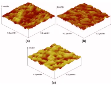
previous reports, the roughness of the gate dielectric/poly-Si inter-face has been reported to affect the on-state characteristic of the TFT device.24The electrical characteristics and reliability of the gate di-electric are also correlated with the surface morphology of poly-Si film.25To investigate the degradation of the on-state characteristic for the 20 W CF4plasma-treated sample, the surface morphology of poly-Si films is analyzed by atomic force microscopy共AFM兲. Fig-ures 8a-c show the AFM images for the poly-Si films with 0, 10, and 20 W CF4plasma treatments, respectively. The average root-mean-square共rms兲 values for poly-Si roughness with 0, 10, and 20 W CF4 plasma treatments were 0.25, 0.31, and 0.47 nm, respectively. Clearly, the poly-Si film with a 20 W CF4plasma treatment shows a
rougher surface morphology, leading to more damage to the integ-rity of the poly-Si channel film. The plasma-etching-induced dam-age to the poly-Si film becomes more obvious with increasing rf power to 20 W. The effect of increasing surface roughness com-pletely dominates the effect of fluorine passivation of trap states, thereby leading to the degraded electrical characteristics.
Figure 9 shows the activation energy共EA兲 of the drain current as
a function of the gate voltage at VDS= 0.1 V for the poly-Si Pr2O3
TFT without共0 W兲 and with 10 and 20 W CF4plasma treatment.
Measurements of the IDS–VGS characteristics are performed on all
the devices for temperatures varying from 25 to 150°C in order to extract the variations of the activation energy of the drain current.26 The value of EA reflects the carrier-transport barrier of the grain
boundary within the poly-Si channel; the higher the EAin the turn-off state, the higher the carrier-transport barrier of the grain bound-ary. An optimal rf power of 10 W CF4plasma treatment can greatly passivate the trap states to reduce the off-state GIDL current and hence exhibit the highest EA in the off state. The implication is consistent with the above extracted data of trap-state density.
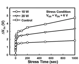
Finally, the influence of electrical stress on poly-Si Pr2O3TFTs with various rf powers of CF4plasma treatments is examined. Fig-ures 10 and 11 show the threshold voltage shift and variation of on current as a function of hot-carrier stress time for the poly-Si Pr2O3 TFTs with 0, 10, and 20 W CF4plasma treatments. The TFT devices
Figure 7. Plot of ln关IDS/共VGS–VFB兲兴 vs 1/共VGS–VFB兲2under strong inversion at VDS= 0.1 V for poly-Si Pr2O3TFTs with various rf powers of CF4plasma treatments.
Figure 8.共Color online兲 AFM images of poly-Si films with various rf
pow-ers of 共a兲 0 共control兲, 共b兲 10, and 共c兲 20 W CF4 plasma treatments. The corresponding rms values of poly-Si surface roughness are 0.25, 0.31, and 0.47 nm, respectively.
Figure 9. Activation energy共EA兲 of the poly-Si Pr2O3TFTs with various rf powers of CF4plasma treatments.
were bias-stressed at room temperature under VGS= 6 V and VDS
= 6 V. The VTH shift and variation of Ion were defined as
共VTH,stressed–VTH,initial兲 and 共Ion,stressed–Ion,initial兲/Ion,initial⫻ 100%,
re-spectively, where the index of the initial and stressed represent the extracted values before and after stresses. The TFT devices with CF4
plasma treatments show smaller VTHshift and variation of Ionthan
that without CF4plasma treatment. Notably, the VTHshift and
varia-tion of Ionof poly-Si Pr2O3TFT with 10 W CF4plasma treatment
are found to be 1.84 V and 16.06% after 1000 s stress, which are superior to those without CF4 plasma treatment 共4.72 V and
38.34%, respectively兲. It has been reported that the degradation of electrical characteristics under hot-carrier stress is attributed to the following two conditions: the generation of gate dielectric/poly-Si interface states and the easily broken weak Si–Si and Si–H bonds in the poly-Si channel.13,14Thus, introducing fluorine atoms into the poly-Si film by CF4plasma treatment would result in the passivation of trap states and the formation of stronger Si–F bonds in place of the weak Si–Si and/or Si–H bonds, exhibiting superior endurance against hot-carrier stress.
Conclusion
We have fabricated and characterized the fluorine-passivation ef-fect on poly-Si TFTs incorporating high- Pr2O3as gate dielectric.
Poly-Si TFT with Pr2O3 gate dielectric can obtain thin EOT and
the poly-Si channel and at the Pr2O3 gate dielectric/poly-Si
inter-face.
Acknowledgments
The authors acknowledge apparatus support from National Nano Device Laboratories共NDL兲 and financial support by the National Science Council共NSC兲 under contract no. NSC 95-2221-E-009-279.
National Chiao Tung University assisted in meeting the publication costs of this article.
References
1. T. Serikawa, S. Shirai, A. Okamoto, and S. Suyama, IEEE Trans. Electron Devices,
36, 1929共1989兲.
2. Y. Oana, J. Soc. Inf. Disp., 9, 169共2001兲.
3. B. D. Choi, H. S. Jang, O. K. Kwon, H. G. Kim, and M. J. Soh, IEEE Trans.
Consum. Electron., 21, 100共2000兲.
4. T. Aoyama, G. Kawachi, N. Konishi, T. Suzuki, Y. Okajima, and K. Miyata, J.
Electrochem. Soc., 136, 1169共1989兲.
5. A. Takami, A. Ishida, J. Tsutsumi, T. Nishibe, and N. Ibaraki, in Proceedings of the
International Workshop on AM-LCD, p. 45共2000兲.
6. C. K. Yang, C. L. Lee, and T. F. Lei, IEEE Electron Device Lett., 16, 228共1995兲. 7. Z. Jin, H. S. Kwok, and M. Wong, IEEE Electron Device Lett., 19, 502共1998兲. 8. M. Y. Um, S.-K. Lee, and H. J. Kim, in Proceedings of the International Workshop
on AM-LCD, p. 45共1998兲.
9. Y. Morimoto, Y. Jinno, K. Hirai, H. Ogata, T. Yamada, and K. Yoneda, J.
Electro-chem. Soc., 144, 2495共1997兲.
10. I. W. Wu, W. B. Jackson, T. Y. Huang, A. G. Lewis, and A. Ciang, IEEE Electron
Device Lett., 12, 181共1991兲.
11. I. W. Wu, W. B. Jackson, T. Y. Huang, A. G. Lewis, and A. Ciang, IEEE Electron
Device Lett., 11, 167共1990兲.
12. H. N. Chern, C. L. Lee, and T. F. Lei, IEEE Trans. Electron Devices, 41, 698 共1994兲.
13. C. K. Yang, T. F. Lei, and C. L. Lee, J. Electrochem. Soc., 143, 3302共1996兲. 14. H. J. Osten, J. P. Liu, P. Gaworzewski, E. Bugiel, and P. Zaumseil, in Tech. Dig.
-Int. Electron Devices Meet., 2000, 653.
15. H. J. Mussig, H. J. Osten, E. Bugiel, J. Dabrowski, A. Fissel, T. Guminskaya, K. Ignatovich, J. P. Liu, P. Zaumseil, and V. Zavodinsky, IRW Final Report, IEEE, p. 1共2001兲.
16. C. W. Chang, C. K. Deng, H. R. Chang, and T. F. Lei, IEEE Electron Device Lett., Accepted.
17. C. H. Tseng, T. K. Chang, F. T. Chu, J. M. Shieh, B. T. Dai, H. C. Cheng, and A. Chin, IEEE Electron Device Lett., 6, 333共2002兲.
18. K. M. Chang, W. C. Yang, and C. P. Tsai, IEEE Electron Device Lett., 24, 512 共2003兲.
19. B. H. Lee, Y. Jeon, K. Zawadzki, W. J. Qi, and J. Lee, Appl. Phys. Lett., 74, 3143 共1999兲.
20. J. Levinson, F. R. Shepherd, P. J. Scanlon, W. D. Westwood, G. Este, and M. Rider,
J. Appl. Phys., 53, 1193共1982兲.
21. R. E. Proano, R. S. Misage, and D. G. Ast, IEEE Trans. Electron Devices, 36, 1915共1989兲.
22. C. A. Dimitriadis, P. A. Coxon, L. Dozsa, L. Papadimitriou, and N. Economou,
IEEE Trans. Electron Devices, 39, 598共1992兲.
23. L. S. Wang, P. C. Wei, T. S. Chang, Y. P. Chang, C. L. Yen, W. C. Yang, and H. Kuan, in Proceedings of International Symposium on Plasma Process-Induced
Damage, p. 29共2001兲.
24. K. Takechi, H. Uchida, and S. Kaneko, in Mater. Res. Soc. Symp. Proc., 1992. 955. 25. J. Y. Lee, C. H. Han, and C. K. Kim, in Tech. Dig. - Int. Electron Devices Meet.,
1994. 523.
26. C. L. Fan and M. C. Chen, Electrochem. Solid-State Lett., 5, 75共2002兲.
Figure 10. Threshold voltage shift vs hot-carrier stress time for poly-Si
Pr2O3TFTs with various rf powers of CF4plasma treatments.
Figure 11. Variations of on current vs hot-carrier stress time for poly-Si