國 立 交 通 大 學
電控工程研究所
碩
碩
碩
碩 士
士
士
士 論
論
論
論 文
文
文
文
0.5V 低功率全數位鎖相迴路設計
低功率全數位鎖相迴路設計
低功率全數位鎖相迴路設計
低功率全數位鎖相迴路設計
A 0.5V Low Power All-Digital Phase-Locked Loop
研 究 生:楊于昇
指導教授:蘇朝琴 教授
0.5V 低功率全數位鎖相迴路設計
A 0.5V Low Power All-Digital Phase-Locked Loop
研 究 生:楊于昇 Student : Yu-Sheng Yang
指導教授:蘇朝琴 教授 Advisor : Chau-Chin Su
國 立 交 通 大 學
電控工程研究所
碩士論文
A ThesisSubmitted to Institute of Electrical Control Engineering College of Electrical Engineering and Computer Science
National Chiao Tung University in partial Fulfillment of the Requirements
for the Degree of Master
in
Electrical Control Engineering June 2011
Hsinchu, Taiwan, Republic of China
0.5V 低功率全數位鎖相迴路設計
研究生 : 楊于昇 指導教授 : 蘇朝琴 教授
國立交通大學電控工程研究所
摘 要
近年來由於環保意識的抬頭,對於手持式產品而言,低功耗成為了電路設計的趨 式。另外半導體的發展使得電晶體的臨界電壓有大幅的下降,但在低功耗的設計中,電 源電壓下降的速度確高於電晶體臨界電壓下降的幅度。因此在低電壓操作下,電路設計 勢必面臨許多問題。對鎖相迴路而言,低電壓操作造成電晶體閘極-源極間電壓減小, 使得電流趨動力大幅下降,因此會限制振盪器的操作頻率。除此之外,當操作電壓下降 至電晶體臨界電壓附近時,電路對於製程變異會變得非常的敏感,效能易受製程影響。 在此論文中,我們提出一個使用拔靴帶式延遲單元(bootstrapped delay cell)的數位控制振 盪器於全數位鎖相迴路中。由於拔靴帶式延遲單元的特性,振盪器的輸出擺幅將被放大 從-VDD至 2VDD。比起由傳統反向器構成的振盪器,此被放大的振幅不僅使得電晶體趨 動力變強,讓振盪器能有較高速的操作,也可使振盪器延遲單元的每顆電晶體遠離次臨 界區的操作,如此一來能降低對於製程變異的敏感度。最後基於這個使用拔靴帶式延遲 單元的振盪器,我們實現了一個低功耗的全數位鎖相迴路,使用 90 奈米製程,晶片面 積為 0.057mm2,其操作電壓為 0.5V,操作頻率範圍(locking range)為 240MHz~480MHz, 當輸出為 400MHz 時,其峰對峰值的抖動(peak-to-peak jitter)為 69.1 ps,而功率消耗僅 70 Wµ 。關鍵字: 全數位鎖相迴路(ADPLL)、拔靴帶式延遲單元(bootstrapped delay cell)、低 功率鎖相迴路(low power PLL)
A 0.5V Low Power All-Digital Phase-Locked Loop
Student: Yu-Sheng Yang Advisor: Chau-Chin Su
Institute of Electrical Control Engineering
National Chiao Tung University
Abstract
In recent years, low power designs for portable devices become popular. Many consumer electronics are asked to consume as less power as possible to extend the battery lifetime. Owing to the progress in CMOS technology, the threshold voltage of the transistor keeps degrading. But the degrading of the system supply voltage is much faster. Under the low power supply environment, the gate-source voltage decreases which leads to the decay of the driving ability. Hence the operation frequency of digital circuit is limited. Besides, the system suffers from process variation badly when the supply voltage is near the threshold voltage of the transistors. For the ADPLL systems, low power supply decreases the operation frequency of the oscillator. So we propose a bootstrapped delay cell for the digitally-controlled oscillator in ADPLLs. With the bootstrapped cell, the output swing of the oscillator is –VDD to 2VDD.
This enlarged swing not only enhances the driving ability but keeps the transistors operate at super VTH region. The circuit then suffers less from the process variation compared to the
oscillators composed of the traditional inverters. Finally, our ADPLL is fabricated in 90nm CMOS technology. The core area is 0.057 mm2. Under supply voltage of 0.5V, the locking range is 240 MHz to 480 MHz. The peak-to-peak jitter is measured 69.1 ps while operating at 400 MHz, and the power consumption is 70 Wµ .
誌
誌
誌
誌謝
謝
謝
謝
首先要感謝我的指導教授蘇朝琴老師,不管是在研究上或待人處事方面都給了我們 很多寶貴的經驗,還教我們不能光靠模擬作研究,模擬只是驗証自己想法的工具。另外 還要感謝博班學長長官、盈杰、仁乾、丸子、庭佑的幫忙,仁乾學長在 PLL 方面給我很 大的幫助,總是不厭其煩地解答我的問題,而盈杰學長在我摸不清研究方向的時候指引 了我一條路,如果沒有他的幫忙,絕不可能完成晶片的下線及量測。除此之外,孔哥、 挺毅、雅婷、子俞、碩廷、教主、譯賢在學術方面都提供了我很多的經驗,也要感謝他 們。而我也要感謝我的好同學洲銘、家齊不只學術上可以一起討論一起修課,生活上也 一起玩樂聊天抒解壓力。接下來我要感謝室驗室的學弟妹修銘、群育、哲瑋、YAS 成員 土豆、精液、昶志、順煜、弘宇、璟伊、澤勝、馬克、AMON、小紅豆、嘉哲、可謙為我 枯躁的研究生活帶來許多的樂趣。 最後我要感謝我的家人,爸爸、媽媽、于政、以健,在物質上與精神上都給了我莫 大的幫助,讓我無後顧之憂的順利完成學業。 2011 06 27 楊于昇Tables of Content
摘
摘
摘
摘 要
要
要
要 ... i
Abstract ... ii
Tables of Content ... iii
List of Figures ... vi
List of Tables ... viii
Chapter 1 ...1
Introduction...1
1.1 Motivation...1 1.2 Challenges...2 1.3 Organization...3Chapter 2 ...4
PLL Fundamentals ...4
2.1 Introduction to Different Types of PLL...4
2.1.1 Analog PLL...4
2.1.2 Charge Pump PLL ...6
2.1.3 All-Digital PLL...11
2.2 Architectures of Low Power Oscillator...13
2.2.1 0.6~1.2V Current-Controlled Oscillator [4] ...13
2.2.2 VCO Using Bulk-Driven Technique [6]...14
2.2.3 Ultra-Low-Power and Portable DCO [7]...17
2.3 Other ADPLL Architectures ...19
2.3.1 Low Jitter ADPLL [8]...19
2.3.2 Wide Frequency Range ADPLL [9] ...20
2.3.3 Low Noise, Wide Bandwidth ADPLL [10] ...22
Chapter 3 ...25
Digitally-Controlled Oscillator with Bootstrapped Delay Cells...25
3.1 Bootstrap Delay Cell...25
3.2 Derivative of Oscillating Frequency...31
3.3 Digitally-Controlled Oscillator ...35
Chapter 4 ...38
Low Voltage 400MHz ADPLL Design ...38
4.1 System Architecture...38
4.2 ADPLL System Analysis [14] ...39
4.2.1 S-Domain Model of ADPLL ...39
4.2.2 Calculation of the DLF Parameters ...42
4.3 Sub-Circuits of the ADPLL System ...44
4.3.1 Phase-Frequency Detector ...44
4.3.2 Phase Selector ...45
4.3.3 Time-to-Digital Converter ...46
4.3.4 Sigma-Delta Modulator ...48
Chapter 5 ...51
Layout, Simulation, and Measurement ...51
5.1 Chip Layout and Simulation ...51
5.2 Measurement Environment Setup...54
5.3 Measurement Results ...56
5.4 Comparison ...60
Chapter 6 ...63
Conclusion ...63
List of Figures
Fig. 2-1: Analog PLL linear model ...5
Fig. 2-2: Charge pump PLL block diagram ...6
Fig. 2-3: Behavior of PFD ...7
Fig. 2-4: (a) Transfer curve of PFD, (b) Dead zone of PFD. ...7
Fig. 2-5: PFD, charge pump, and loop filter ...8
Fig. 2-6: Operation of the charge pump...8
Fig. 2-7: 1st order, 2nd order, and 3rd order filter ...9
Fig. 2-8: Characteristic curve of VCO...9
Fig. 2-9: Voltage-controlled ring oscillator ...10
Fig. 2-10: LC tank oscillator...11
Fig. 2-11: All-digital phase-locked loop...12
Fig. 2-12: Differential delay element of current-controlled oscillator [4] ...13
Fig. 2-13: Comparison between gate- and bulk- driven [6]...15
Fig. 2-14: Circuit configuration of the bulk-driven VCO [6] ...16
Fig. 2-15: Architecture of proposed DCO [7]...17
Fig. 2-16: Coarse tuning stage [7] ...17
Fig. 2-17: Fine tuning stage [7] ...17
Fig. 2-18: Low jitter ADPLL architecture [8]...19
Fig. 2-19: DCO architecture [8]...20
Fig. 2-20: Wide frequency range ADPLL [9] ...21
Fig. 2-21: DCO structure [9]...22
Fig. 2-22: Low noise and wide loop bandwidth ADPLL [10] ...23
Fig. 2-23: Time-to-digital converter [10]...23
Fig. 3-1: Proposed bootstrap delay cell ...26
Fig. 3-2: Operation of the cell (input from high to low)...27
Fig. 3-3: Operation of the cell (input from low to high)...27
Fig. 3-4: Waveforms of each node in proposed delay cell...28
Fig. 3-5: (a) Proposed cell in [12] (b) primary boosting cell ...29
Fig. 3-6: Parasitic capacitor and boosting capacitor equivalent circuit ...30
Fig. 3-7: Boosting capacitor verses VB...30
Fig. 3-8: Waveform of a three-stage ring oscillator ...31
Fig. 3-9: Propagation delay calculation (high to low) ...33
Fig. 3-10: Propagation delay calculation (low to high) ...34
Fig. 3-11: Architecture of DCO ...35
Fig. 3-12: Voltage control circuit of DCO ...35
Fig. 3-13: Simulation of the DCO transfer curve ...36
Fig. 4-1: ADPLL architecture ...39
Fig. 4-2: S-domain model of ADPLL ...40
Fig. 4-3: S-domain model of CPPLL...40
Fig. 4-4: Implementation of DLF from analog filter ...42
Fig. 4-5: Bode Plot of the 2nd order ADPLL...43
Fig. 4-6: (a) Phase-frequency detector, (b) half transparent register ...45
Fig. 4-7: (a)FREF leads FB, (b)FB leads FREF...45
Fig. 4-8: Phase selector ...46
Fig. 4-9: Operation of the phase selector (a) FREF leads FB, (b) FB leads FREF...46
Fig. 4-10: 4-bit vernier TDC ...47
Fig. 4-11: Phase comparator ...47
Fig. 4-12: Simulation result of the 4-bit Vernier TDC...48
Fig. 4-13: Block diagram of 1st order SDM...48
Fig. 4-14: Discrete time signal flow diagram ...49
Fig. 4-15: All digital 1st order SDM...50
Fig. 5-1: Chip layout ...52
Fig. 5-2: Layout of ADPLL ...52
Fig. 5-3: Post-layout simulation of the ADPLL...53
Fig. 5-4: Die photo...55
Fig. 5-5: PCB layout ...55
Fig. 5-6: Measurement Setup...56
Fig. 5-7: DCO free-running @ 0.5V...56
Fig. 5-8: ADPLL locked @ 240 MHz...57
Fig. 5-9: ADPLL locked @ 320 MHz...57
Fig. 5-10: ADPLL locked @ 400 MHz...58
Fig. 5-11: ADPLL locked @ 480 MHz...58
Fig. 5-12: Power consumption and jitter at different frequency...59
Fig. 5-13: FOM1 versus operation frequency ...62
List of Tables
Table 2-1: Comparison of different PLL ...12
Table 3-1: The DCO gain at different corners ...37
Table 4-1: Parameters of ADPLL ...44
Table 4-2: Oscillating period change due to SDM dithering ...49
Table 5-1: The input and output pins of the chip ...53
Table 5-2: Post-layout simulation results ...54
Table 5-3: Output performance of different supply voltage ...59
Table 5-4: Chip summary ...60
Chapter 1
Introduction
1.1 Motivation
As the CMOS technology develops rapidly, the transistor number in one chip increases tremendously. Many complicated circuits with different function can be integrated on a chip. That’s why the concept of System-on-Chip (SOC) becomes more and more popular. So the synchronization of clocks among different modules becomes important. First, there is a reference frequency from external crystal oscillator. This external clock is used as the reference clock for all the Phase-Locked Loops (PLL). PLLs provide the synchronized clocks for all the modules in the system to prevent errors from clock skews. In addition, PLLs can also work as frequency synthesizers to provide variety of clock frequencies to meet the system requirement.
In recent years, eco-awareness gains ground. A lot of electronic products are required to consume as less power as possible to extend the life time of batteries. In PLL systems, the most power consuming block is the oscillator which operates at the highest frequency in the system. If one wants to realize a low power PLL, the most efficient method is to reduce the power of the oscillators. Since the power consumption of an oscillator is proportional to the supply voltage (VDD) of the system, the most straightforward way to reduce the power
consumption is to reduce the supply voltage of the system.
1.2 Challenges
When we reduce the supply voltage of the circuits, many problems arise. Owing to the reduction of supply voltage, the gate-source voltage (V ) of the MOSFETs decreases, and so GS does the overdrive voltage (VGS−VTH) of the transistors. So the drain current of the transistors decreases under low supply voltage environment. It leads to the increase of rise time and fall time of the transistors. Hence, the operation frequency of the circuit is limited at low supply voltage. Generally speaking, the threshold voltage (V ) of the transistors in TH 90nm CMOS is about 0.26V. When the supply voltage goes down near V , the circuit may TH become more sensitive to the process variation. Especially for the oscillator, the linearity becomes worse and it may fail at SS corner.
In this thesis, we propose a bootstrapped cell for the digitally-controlled oscillator (DCO) being designed. By the characteristic of bootstrapped cell, the output swing of the DCO is
DD
V
− to2VDD. This wider output swing not only enhances the driving ability of cell output, but also makes the transistors operate at super threshold region. So the linearity of DCO curve is better than those in the sub-threshold region. The supply voltage we use here is 0.5V which is the output voltage of a solar cell, so with this bootstrapped cell we can achieve higher operating frequency and reduce the overall power consumption substantially.
1.3 Organization
This thesis comprises six chapters. The motivation and features are described in this chapter. Chapter 2 describes the background studies. It starts with an overview of the basic PLL systems. Then, we introduce the architectures of the low power oscillators. Finally, we introduce the different architectures of ADPLLs.
Chapter 3 addresses the architecture of the proposed bootstrapped delay cell and analyzes its behavior. The oscillation frequency is also discussed. Based on this discussion, the DCO consisting of the bootstrapped delay cells is implemented. Chapter 4 depicts the linear model of the ADPLL. With this approximation, we can design the ADPLL parameters for the stability of the feedback system.
Chapter 5 shows the layout and post-layout simulations of the ADPLL. Measurement environment is also presented in this chapter. The measured results and the comparison table are depicted as well. Finally, Chapter 6 concludes this thesis.
Chapter 2
PLL Fundamentals
2.1 Introduction to Different Types of PLL
In this chapter, we’re going to introduce three types of PLLs. They are analog PLL (APLL), charge pump PLLs (CPPLL), and all digital PLLs (ADPLL) respectively. The first PLL model was proposed by a French engineer Bellescize in 1930. It is commonly used in clock generator, clock and data recovery (CDR), and frequency synthesizer circuits, which are the important circuits in modern electronic industry.
2.1.1 Analog PLL
Analog PLL is composed of three basic analog blocks, a phase detector (PD), a loop filter, and a voltage-controlled oscillator (VCO). The block diagram of an APLL is shown in Fig. 2-1.
Fig. 2-1: Analog PLL linear model
The phase detector compares the phase of the reference input clock with the oscillator feedback signal. The detected phase error is multiplied by a gain of K , so it comes out with D a voltage which represents the phase error between the reference input clock and the feedback signal. The output of PD is given by
d D e D i o
U (s)=K θ (s)=K [ (s) -θ θ (s)]
. (2.1) The loop filter is usually an active or passive low pass filter to filter out the high frequency input noises. It provides a DC control voltage to VCO to have it oscillate at the desired frequency. As for the VCO, it converts the control voltage from loop filter to an output frequency. The VCO behavior is like an integrator with a DC gain of KVCO. Its transfer function is given by f VCO o U (s) K (s) s × θ = . (2.2)
So the transfer function of the analog PLL is expressed as
o D VCO i D VCO (s) K K F(s) H(s)= (s) s K K F(s) θ = θ + , (2.3)
where F(s) is the transfer function of the loop filter. It should be noted that in analog PLL the output frequency is the same as the input reference frequency.
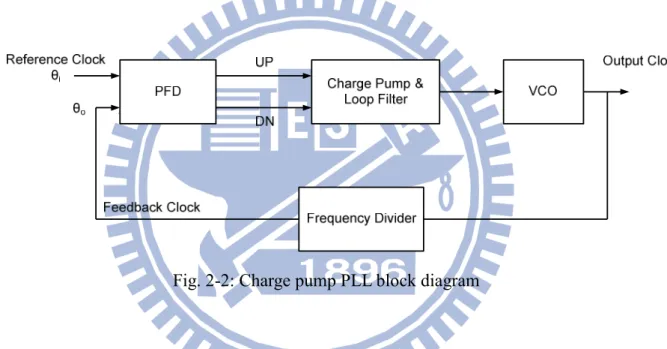
2.1.2 Charge Pump PLL
A charge pump PLL is also known as a digital PLL. It is usually composed of a phase frequency detector (PFD), a charge pump, a frequency divider, a loop filter and a VCO. The block diagram is shown in Fig. 2-2. PFD detects the phase and frequency error between the reference clock and the feedback clock to produce a lead/lag signal to the charge pump. Based on the lead/lag signal, the charge pump charges or discharges the loop filter to adjust the control voltage of the VCO. In CPPLL, a frequency divider is often inserted. So the frequency multiplication can be achieved. Each block will be briefly introduced in the next paragraphs.
Fig. 2-2: Charge pump PLL block diagram
PFD detects the phase error of two different signals to produce an output impulse which is proportional to the phase difference, as shown in Fig. 2-3. When θ leads i θ , the impulse o signal UP is produced whose width is equal to the phase difference of θ and i θ , as shown o in Fig. 2-3(a). On the contrary, the DN signal appears when θ leads o θ , as illustrated in Fig. i 2-3(b). The transfer curve of PFD is shown in Fig. 2-4(a). The dead zone is a key point of PFD, which is shown in Fig. 2-4(b). Dead zone is the region that PFD fails to produce UP or DN signal to the charge pump. It may result in large timing jitter in the output clock.
Fig. 2-3: Behavior of PFD
Fig. 2-4: (a) Transfer curve of PFD, (b) Dead zone of PFD.
The charge pump shown in Fig. 2-5 consists of two current sources and two switches. When A has a higher frequency than B or lead in phase at the same frequency, the UP signal will turn the switch S1 on. Current I1 will charge the capacitor CP. It results in the increase of
the output voltage as shown in Fig. 2-6. Otherwise, S2 is turned on. CP is discharged by I2 and
the output voltage drops. The transfer function of the PFD and the charge pump is
e PUMP I I 2 φ = × π (2.4)
where IPUMP is the output current of the charge pump and I=I1=I2 is the current of two current
frequency (usually 1/10~1/15) can equation (2.4) be approximated to a continuous-time system. CP Vout I1 I2 IPUMP UP DN VDD PFD A B S1 S2
Fig. 2-5: PFD, charge pump, and loop filter
Fig. 2-6: Operation of the charge pump
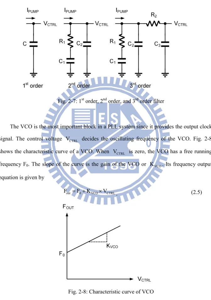
The Loop filter decides the stability of a PLL system. It is implemented in either active or passive manner. The passive one has better ability to filter the noise and is also easier to design. So the passive filter is usually used in most PLL systems. Fig. 2-7 shows the first order, second order, and third order loop filters respectively. VCTRL is the control voltage for
the VCO.
Fig. 2-7: 1st order, 2nd order, and 3rd order filter
The VCO is the most important block in a PLL system since it provides the output clock signal. The control voltage VCTRL decides the oscillating frequency of the VCO. Fig. 2-8 shows the characteristic curve of a VCO. When VCTRL is zero, the VCO has a free running frequency F0. The slope of the curve is the gain of the VCO or KVCO. Its frequency output
equation is given by
out 0 VCO CTRL
F =F +K ×V
. (2.5)
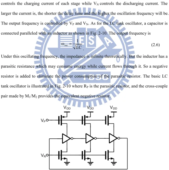
There are two major structures of the oscillators. One is the ring oscillator and another is the LC tank oscillator. A ring oscillator has a wider frequency tuning range and occupies smaller chip area. But its phase noise is high. A LC tank oscillator takes the advantage of low phase noise and high operating frequency, however it occupies more area since it’s composed of capacitors and inductors. So designers must choose the structure of oscillator by their specifications and application needs.
A basic single-ended voltage-controlled ring oscillator is illustrated in Fig. 2-9. VP
controls the charging current of each stage while VN controls the discharging current. The
larger the current is, the shorter the delay time and the higher the oscillation frequency will be. The output frequency is controlled by VP and VN. As for the LC tank oscillator, a capacitor is
connected paralleled with an inductor as shown in Fig. 2-10. The output frequency is
osc
1 LC ω =
. (2.6)
Under this oscillating frequency, the impedance is infinite theoretically. But the inductor has a parasitic resistance which may consume energy while current flows through it. So a negative resistor is added to eliminate the power consumption of the parasitic resistor. The basic LC tank oscillator is illustrated in Fig. 2-10 where RP is the parasitic resistor, and the cross-couple
pair made by M1/M2 provides the equivalent negative resistor.
RP -R VDD L RP L C M1 M2 C
Fig. 2-10: LC tank oscillator
2.1.3 All-Digital PLL
The ADPLL is composed of digital circuits only, as shown in Fig. 2-11. Traditional charge pumps are replaced by a time-to-digital converter (TDC). TDC converts the phase difference between the reference clock and the feedback clock into digital codes. The digital code is fed into the loop filter. The digital loop filter (DLF) substitutes the traditional analog loop filter. The output clock is provided by a digitally-controlled oscillator (DCO) whose input signal is given by the digital loop filter. ADPLLs take advantage of small area occupation, and better stability, but suffers from lower output frequency and higher output jitter. The detail of each block of an ADPLL will be discussed in Chapter 3 and Chapter 4. Table 2-1 demonstrates the comparison of different types of PLL.
Fig. 2-11: All-digital phase-locked loop
Table 2-1: Comparison of different PLL
APLL CPPLL ADPLL Noise Immunity Low Low High Power Consumption High High Low Area Large Large Small Output Frequency High High Low Oscillator Resolution High High Low
2.2 Architectures of Low Power Oscillator
The most power consuming block in a PLL system is the oscillator since it operates at the highest frequency in the system. So reducing the power consumption of the oscillator is the most efficient way to decrease the system power. In this section, some low power VCOs and DCOs will be outlined.
2.2.1 0.6~1.2V Current-Controlled Oscillator [4]
In order to achieve a wide range of power-supply operation without introducing a secondary higher power supply, a clock generation architecture needs to be able to operate down to sub-1V regions. CMOS ring oscillator based on the self-biased architecture [1] requires a voltage headroom of VDD >VTH+2VDSAT for operation. Existing current-controlled oscillator [2] also has similar voltage headroom requirements. Current-starved inverter ring oscillator [3] has a VDD requirement of VTH+VDSAT. The PLL presented in [4] is based on a single VTH current-controlled oscillator, which still require enough voltage headroom for low power supply applications.
The basic delay cell used in [4] is shown in Fig. 2-12. MN1/ MN 2 and MN1'/ MN 2' form a complementary differential pair that are driven by current sources M and P1 M . The P2 swing of the differential output and input nodes depends on the bias current IBIAS, the voltage drop across MP1,2, and the size of the differential load devices. When the delay cells are connected in ring oscillator, VO,MAX =VDD−| VDSATP| and VO,MIN =| VDSATN|, where VDSATP and VDSATN are the drain-source saturation voltages of M and P1 MN1,2 respectively under a given bias current IBIAS. Therefore the high-low and low-high transition delay can be expressed as N1 N 2 L swing L L PHL M M BIAS C V C C t gm gm I ⋅ ∆ = + ≈ (2.7) L swing PLH BIAS C V t I ⋅ ∆ ≈ (2.8)
where ∆Vswing= (VO,MAX - VO,MIN). Thus, for an N-stage ring oscillator the frequency of
oscillation is BIAS cco L swing I f 2N C V ≈ ⋅ ⋅ ∆ , (2.9) P1 N1,2 BIAS BIAS swing DD M M I I V V ∆ = − − β β . (2.10)
Above equations imply that VDD can be scaled down to VDD,MIN =max(| VTHP|, VTHN). This is the minimum requirement in maintaining the switching capability of the ring oscillator.
2.2.2 VCO Using Bulk-Driven Technique [6]
One important solution to the threshold voltage limitation is the bulk-driven technique. It is a typical technique to the operational amplifier design in low-voltage [5]. The bulk-driven MOSFET allows zero, negative, and even small positive bias voltage to achieve the desired
DC current. It also extends the input common-mode range which is difficult to achieve at low supply voltage. Typically, the bulk terminals of MOSFETs are always connected to the highest (or lowest) voltage in the circuit for PMOS (or NMOS) transistors to avoid the latch-up problem. In a 0.5-V design, no risk of forward biasing of this junction exists. The bulk terminal can be used with a rail-to-rail input.
Fig. 2-13: Comparison between gate- and bulk- driven [6]
Fig. 2-13 shows the characteristics of the gate- and bulk- driven PMOS transistors. In the gate-driven PMOS without forward body biasing (FBB), the source-to-gate voltage must be greater than the absolute value of the threshold voltage while in the bulk-driven technique, it can eliminate the above limitation.
Fig. 2-14: Circuit configuration of the bulk-driven VCO [6]
In [6], a bulk-input technique is employed to implement a VCO to improve the operating frequency at lower supply voltage. Fig. 2-14 shows the circuit configuration of the VCO. It consists of three stages of fully differential cells. The NMOS transistors (M1, M2) in the delay
element are used in a positive feedback topology to reduce the transition time of the output and ensure the logic state. The bulk terminals of the PMOS transistors in the delay elements are directly controlled by the loop filter output voltage VCTRL. Therefore, the bulk-input
technique can extend the dynamic range of the control voltage to rail-to-rail to provide a highly linear gain without a V-I converter. In addition, the current source IVCO is
digitally-controlled by a 2-bit word from the calibration circuit to prevent PVT variations and maintain the desired operating frequency.
2.2.3 Ultra-Low-Power and Portable DCO [7]
Fig. 2-15: Architecture of proposed DCO [7]
Fig. 2-16: Coarse tuning stage [7]
Fig. 2-15 illustrates the architecture of an ultra-low-power DCO in [7]. The main idea of [7] is to change the oscillating frequency by means of modifying the delay time of the signal path. To preserve the control code resolution and the operation range, the DCO employs a cascade structure consisting of coarse-tuning and fine-tuning stages. Therefore, the control code-to-delay linearity and operating range can be achieved easily. Two low-power techniques are obtained in [7]. First, the segmental delay line (SDL) can disable the transition of redundant segmental delay cells in coarse-tuning stage, as shown in Fig. 2-16. Second, the hysteresis delay cell (HDC) is proposed for the fine tuning stage to reduce the number of short-delay cells. The fine tuning stage is shown in Fig. 2-17 which has three sub-fine-tune stages. It is composed of a HDC, a long-delay digitally-controlled varactor (DCV), and a short-delay DCV. In addition, it should be noted that the controllable range in each stage must be larger than the delay step of the previous stage. So the cascade DCO structure doesn’t have any dead zone larger than the LSB resolution of the DCO.
2.3 Other ADPLL Architectures
Three oscillators used in low power PLLs are mentioned in the above section. Since our low power PLL is implemented in all-digital way, we focus on the architectures of ADPLL in the following sections.
2.3.1 Low Jitter ADPLL [8]
In ADPLLs, digital loop filters replace analog loop filters to reduce the area overhead. But an extra adder is required to sum up the proportional and the integral parts of the digital loop filter. As shown in Fig. 2-18, with a mixed-signal PFD, the extra adder is no more needed and the longest transport delay is reduced. In addition, the PFD has a shorter switching time. It is proportional to the phase error. So it has better jitter performance than the bang-bang PFD. As for the DCO, higher frequency resolution of DCO can decrease the output jitter. Thus, a DCO resolution enhancement circuit is applied to achieve the low jitter requirement.
Fig. 2-18: Low jitter ADPLL architecture [8]
Fig. 2-19 shows the architecture of the DCO. To improve the frequency resolution, a 8-bit sigma-delta modulator is applied. Besides, a DCO resolution enhancement circuit is added to
the DCO. It controls one PMOS from the array with the high frequency output of the oscillator to improve the resolution. Without the enhancement circuit, the on- or off-time of the control signal from sigma-delta modulator is beyond one reference clock period. On the other hand, the equivalent on- or off-time is halved with the enhancement circuit, which means the equivalent frequency resolution is doubled.
D5 D6 D11 D5 VDD D1 D2 D3 D4 Resolution Enhancement D0 DDSM
Three-Stage Ring Oscillator
OUT1-OUT1+ OUT2-OUT2+ OUT3-OUT3+ Vsupply UP DN FOUT
Fig. 2-19: DCO architecture [8]
2.3.2 Wide Frequency Range ADPLL [9]
The ADPLL in [9] is implemented in a single-loop structure which is shown in Fig. 2-20. Based on the binary bang-bang PFD, a third-order sigma-delta modulator and a programmable proportional-integral-differential loop filter are introduced. The ring oscillator based DCO consists of the tri-state inverters and has 768 frequency output levels to cover the PVT variation. The use of the bang-bang PFD and the array-controlled DCO let the ADPLL system
having a wide supply voltage range as well.
Fig. 2-20: Wide frequency range ADPLL [9]
Fig. 2-21 shows the schematics of the DCO. An inverter array composed of three-stage ring oscillators contains 17 columns and 48 rows. By changing the current driving ability, 768 output frequency levels can be attained aiming for the wide frequency output applications. An accurate DAC or binary-to-thermometer converter is no longer needed here, since the DCO converts the digital codes to output frequency directly. The function of binary-to-thermometer converter can be achieved by controlling the shift of columns and rows inside the DCO.
In ve rte r A rr a y R o w C o n tr o l
Fig. 2-21: DCO structure [9]
2.3.3 Low Noise, Wide Bandwidth ADPLL [10]
The ADPLL in [10] utilizes a high resolution time-to-digital converter to attain wide loop bandwidth and prevent long settling time. Its architecture is shown in Fig. 2-22. Based on a counter-assisted PLL, it does not need a programmable frequency divider to prevent the high frequency noise, which is different from the traditional fractional-N PLL.
Fig. 2-22: Low noise and wide loop bandwidth ADPLL [10]
In the time-to-digital converter, time amplifier is introduced to improve the resolution and decrease the quantization noise. Fig. 2-23 is the TDC mentioned here. It consists of a coarse tuning and a fine tuning stage. When the time difference is less than the delay time of an inverter, the time amplifier enlarges the time difference and passes it into the fine tuning section. In this way, a root mean square resolution less than 1ps is achieved.
2.4 Summary
In Section 2.2, several low power techniques [4], [6], [7] have been presented, but still some problems remain. For instance, the delay cell in [4] cascodes less transistors to have a wider operating supply voltage range. But when the supply voltage goes down to the voltage near the threshold voltage, the current might decrease severely. The bulk-driven technique [6] reduce the threshold voltage of the transistor to get better current driving ability. As the threshold voltage decreases, the leakage current of a turned-off transistor IOFF increases. So
the bulk-driven technique can not solve the leakage current issue under low power supply application. In [7], in order to achieve wide tuning range, a great amount of loading cells are required. These loading cells would result in large leakage current as well.
Chapter 3
Digitally-Controlled Oscillator with
Bootstrapped Delay Cells
The most important block in a ADPLL is the DCO which provides the different output frequency according to the binary control code. In this chapter, we will introduce the proposed DCO with the bootstrap delay cells for low power supply environment.
3.1 Bootstrap Delay Cell
The proposed delay cell shown in Fig. 3-1 is a bootstrap inverter. Transistors MN1, MP1
provide the charging and discharging path for the capacitors. Transistors MN2, MP2 work as
current switches, and inv1, inv2 are the traditional CMOS inverters. Capacitors C1, C2 are the
enhancing the driving ability for the next stage.
Fig. 3-1: Proposed bootstrap delay cell
The operation of the delay cell is illustrated in Fig. 3-2. When the input signal drops from VSUP to 0, the initial voltage across the capacitor C2 makes the drain of the transistor MP1
boost to 2VSUP.The input signal also turns on MP2, and the output node is charged to 2VSUP as
well. At the mean time, the output voltage would turn on MN1, and C1 will be charged until
the voltage across it is VSUP. So C2 provides the boosting voltage, and C1 is reset while the
Fig. 3-2: Operation of the cell (input from high to low)
Fig. 3-3: Operation of the cell (input from low to high)
When the input signal rises from 0 to VSUP as illustrated in Fig. 3-3, the voltage across C1
makes the source of MN2 boosted downward to –VSUP. Then the output node is discharging
to –VSUP. Similar to the operation above, the output voltage turns MP1 on, so C2 is charged
waveforms of each node are shown in Fig. 3-4.
Fig. 3-4: Waveforms of each node in proposed delay cell
As we know, the traditional bootstrapped inverters in [12] [13] suffer from several non-ideal effects. Firstly, the bootstrapped inverter induces the reverse current which may decrease the boosting efficiency. The bootstrapped cell in [12] is illustrated in Fig. 3-5 (a). Fig. 3-5 (b) shows the primary structure of the boosting cell. In Fig. 3-5 (b), when the input signal changes from 0 to VDD, the voltage of VB should be boosted to 2VDD. Owing to the symmetry
of the MOSFET, node B, the terminal with the highest voltage, will become the source of the transistor. Hence the VSG of the transistor produces the reverse current from the boosted node
to the power supply, causing the charge leakage of the capacitor to the power supply. Although the reverse current won’t cost extra power consumption, somehow it will decrease the voltage of VB and make it less than 2VDD. As to the proposed cell in Fig. 3-1, because the
gates of MP1 and MP2 are connected to the output node which is boosted to 2VDD or -VDD, the
gate-source voltage of MP1 and MN1 will not be large enough to turn on MP1 and MN1. In this
efficiency than the ones in [12] and [13].
Fig. 3-5: (a) Proposed cell in [12] (b) primary boosting cell
In addition to the reverse current, the parasitic capacitors can also lead to the degradation of the boosting efficiency. The boosting cell and its equivalent circuit are shown in Fig. 3-6. With the parasitic capacitor CP and the boosting capacitor CB, the voltage variation of VB is
expressed as B B IN B P C V V C C ∆ = ∆ + (3.1)
while VIN is changed by ∆VIN. The value of CP is decided by the sizes of transistors. A small
transistor has small CP. But it has weaker driving ability as well. Hence, reducing CP by using
smaller transistor to reduce CP is not a good approach. Since the value of CP has been fixed,
we have to use larger CB to reach required boosting efficiency. The consequence is the large
(CB), from which the value of CB can be decided.
Fig. 3-6: Parasitic capacitor and boosting capacitor equivalent circuit
0 20 40 60 80 100 120 140 160 0.60 0.65 0.70 0.75 0.80 0.85 0.90 CB (fF) V B H ( V ) -0.45 -0.40 -0.35 -0.30 -0.25 -0.20 -0.15 -0.10 V B L ( V ) 0 20 40 60 80 100 120 140 160 0.60 0.65 0.70 0.75 0.80 0.85 0.90 CB (fF) V B H ( V ) -0.45 -0.40 -0.35 -0.30 -0.25 -0.20 -0.15 -0.10 V B L ( V )
3.2 Derivative of Oscillating Frequency
The simplest ring oscillator is implemented by three inverters. It provides the highest oscillating frequency. Fig. 3-8 shows a three-stage ring oscillator composed of traditional inverters and waveforms of each node. TD is the propagation delay of each stage. Since the
output has a rail-to-rail large signal swing, the oscillating frequency is presented by
osc D 1 f 2NT = . (3.2) N represents the number of stages in the ring oscillator. N must be an odd number to avoid circuit latch up. There are some differential implementations which can utilize even number of stages by simply making one stage without inverts. The number of stages in a ring oscillator is determined by many factors, such as speed, power dissipation, noise immunity, etc. In most applications, three to five stages provides optimum performance.
Fig. 3-8: Waveform of a three-stage ring oscillator
In order to estimate the output frequency of the oscillator, we have to calculate the propagation delay of a single cell. Assume a rising edge from VOL to VOH is applied in the
input node as illustrated in Fig. 3-9, where VOL and VOH are two output voltages of the
bootstrapped cell. Consider the non-ideal effect mentioned above, VOL and VOH can be
B OL SUP B P2 C V ( V ) C C = × − + , (3.3) B OH SUP B P1 C V 2V C C = × + (3.4)
where CP1, CP2 are the parasitic capacitors at nodes VBH and VBL respectively. The output
propagation delay from high to low tPHL can be separated into two periods. In the first period,
the output is discharging from VOH to VOH-Vt, and MN2 is in saturation region. So tPHL1 is
calculated from PHL1 OH t OH T t V V DN L out T i dt V C dV + − − =
∫
∫
DN PHL1 L t i t C ( V ) ⇒ − × = × − L t PHL1 2 n n OH OL t C V t 1 W k ( ) [(V V V ) ] 2 L ⇒ = − − . (3.5) In the second period, the output is lowing from VOH-Vt to 0.5(VOH-VOL) and MN2 operates inDN L out
i dt C dv − =
2
n n OH OL t out out L out
W 1 k ( ) [(V V V )V V ]dt C dV L 2 ⇒ − − − − = n n out 2 L OH OL t out out W k ( ) 1 L dt dV 2C [2(V V V )V V ] ⇒ − = − − − OL OH t OH t L PHL 2 OL OH t n n OH OL t OH OL 3 3 V V 2V V V C 2 2 t ln[ ] W 1 2V V V k ( ) (V V V ) (V V ) L 2 − + − ⇒ = × − + − − − (3.6)
Fig. 3-9: Propagation delay calculation (high to low) From (3.5) and (3.6) the propagation delay tPHL can be expressed by
PHL PHL1 PHL2
t =t +t . (3.7) Similarly the same method can be applied to calculate the propagation delay from low to high tPLH as follows, L t PLH1 2 p p OH OL t C V t 1 W k ( ) (V V V ) 2 L = − − , (3.8)
OL OH t OH OL t L PLH 2 OH OL t p p OH OL t OH OL 5 3 V V 2V V V V C 2 2 t ln[ ] W 1 V V V k ( ) (V V V ) (V V ) L 2 − + − − = × − + + − − − . (3.9) PLH PLH1 PLH 2 t =t +t . (3.10) Once tPHL and tPLH are obtained, the propagation delay of the single stage delay cell is
D PLH PLH
1
T (t t ) 2
= + . (3.11)
After that, the oscillating frequency can be estimated by (3.2). In our design the ring oscillator is composed of 5 stages, so the output frequency is
osc D 1 f 10T = . (3.12)
3.3 Digitally-Controlled Oscillator
The overall DCO architecture is illustrated in Fig. 3-11, which is a 5-stage ring oscillator. According to the previous equations we can control the output frequency by manipulating the supply voltage of the delay cells VSUP. The voltage control circuit plays as a variable resistor
in Fig. 3-12. It adjusts the equivalent resistance REQ to control the VSUP. As shown in Fig.
3-12, the voltage control circuit is composed of PMOS array which is similar to the one in [8]. A 9-bit PMOS array contains 5 bits for coarse tune and 4 bits for fine tune. The least 4 bits are transformed into thermometer code for better linearity. The rest 5 bits remain binary to save the chip area.
Fig. 3-11: Architecture of DCO
In [8] the PMOS array of the voltage control circuit is binary-weighted. The VSUP is given by FIX SUP DD EQ FIX R V V R R = × + (3.13)
where RFIX is the equivalent resistance of the delay cells. From (3.13) we can tell that VSUP
will not have a linear behavior while REQ varies linearly. In ours design the PMOS array is not
binary-weighted. It is designed individually to maintain the linearity of the transfer curve. Fig. 3-13 shows the HSIPCE post-layout simulation of the DCO transfer curve. In addition to the TT corner, the other two extreme corners FF and SS are also simulated to make sure the operation frequency of DCO can work at 400MHz under process variation. The simulation gain of the DCO is about 563 kHz/code at TT corner and the DCO gain of the other corners is listed in Table 3-1. 100 200 300 400 500 600 100M 200M 300M 400M 500M 600M 700M 800M 900M F re q u e n c y ( H z ) Control Codes TT FF SS
Table 3-1: The DCO gain at different corners
TT FF SS FNSP SNFP Gain
(kHz/code)
563 733 843 981 1100 The output frequency of the ring oscillator composed of the traditional inverters is shown in Fig. 3-14. The horizontal axis is the supply voltage and the vertical axis is the oscillation frequency. Fig. 3-14 shows that the linearity degrades while supply voltage goes down. At the SS corner, the oscillator can hardly work around 0.3V. In addition, the gain of output frequency versus supply voltage (KVCO) is high which may lead to the large output jitter for
the PLL. Compared to the traditional one, the boosted output swing (from –VDD to 2VDD)
keeps the transistors from operating in sub-threshold region at low supply voltage. The bootstrapped ring oscillator has better linearity, lower KVCO, and better immunity against
process variation. 0.15 0.20 0.25 0.30 0.35 0.40 0.45 0.50 0.55 0 1G 2G
O
u
tp
u
t
F
re
q
u
e
n
c
y
(
H
z
)
Supply Voltage (V)
inv_TT
inv_FF
inv_SS
bootstrap_TT
bootstrap_FF
bootstrap_SS
Chapter 4
Low Voltage 400MHz ADPLL Design
4.1 System Architecture
The proposed ADPLL architecture is shown in Fig. 4-1. The phase frequency detector (PFD) detects the phase error between the reference clock and the feedback signal. Then the phase error is quantized in a 4-bit binary code in the time-to-digital converter (TDC). The output of TDC is fed into the digital loop filter (DLF) to control the DCO. The 4-bit decimal output of the DLF is fed into the sigma-delta modulator to dither the LSB of the DCO to improve the equivalent DCO resolution. Besides, the divider provides a division ratio of 1/16. In our design the input reference clock is 25MHz, and the output frequency is 400MHz. All sub-circuits will be described later in this chapter.
Fig. 4-1: ADPLL architecture
4.2 ADPLL System Analysis
Since a PLL is a closed-loop system, the system must be maintained stable to have proper operation. In this section, the S-domain system model of ADPLL will be introduced and compared to the traditional CPPLL model. So we can base on the CPPLL analogy to design the ADPLL system parameters.
4.2.1 S-Domain Model of ADPLL
The s-domain approximation for the ADPLL system is shown at Fig. 4-2 [14]. The phase- frequency detector converts the input phase error to an impulse output. The transfer function of the PFD can be approximated as
REF T PFD(s) 2 = π , (4.1)
where TREF is the period of the input reference clock. The output from PFD is digitized by the time-to-digital converter of resolution ∆TDC. The resolution of the TDC is considered
fixed in this analysis and its transfer function can be obtained as
TDC
1 TDC(s) =
∆ . (4.2)
The digital domain phase error is then filtered by the digital loop filter and fed into the DCO with a transfer function given by
DCO
K DCO(s)
s
= . (4.3)
Fig. 4-2: S-domain model of ADPLL
Comparing the model above with the s-domain model of a CPPLL shown in Fig. 4-3, we obtain the following equations,
REF CP TDC T I = ∆ , VCO DCO K =K , Z(s)=H(s). (4.4) So the parameters of a CPPLL can be determined first for a specific specification. Then with (4.4), we can get the corresponding parameters for the ADPLL.
Fig. 4-3: S-domain model of CPPLL
As for the loop filter, a traditional CPPLL usually has a second order loop filter in order to attenuate the ripple caused by the nature of CPPLL. But in ADPLLs, this problem does not exist. So the first order loop filter is sufficient. In the following paragraphs, we will discuss
how to calculate the filter parameters due to a given stability criterion. A first order analog filter can be implemented by a resistor and a capacitor as illustrated in Fig. 4-4. The transfer function is given by
V(s) 1 Z(s) R
I(s) sC
= = + . (4.5) The open loop transfer function of the 2nd order CPPLL is
CP VCO Z I K 1 (s ) G(s) R 2 s N s + ω = π . (4.6)
The zero frequency ω is Z
Z
1 RC
ω = . (4.7)
The phase margin (PM) of the system is
1 UGB Z
PM=tan (− ω )
ω , (4.8)
where ωUGB is the unit gain bandwidth. It is also known as the loop bandwidth in a PLL system. If we have a specific phase margin, the zero frequency ω can be decided from (4.8). Z Based on | G( jωUGB) | 1= , the resistance value R in (4.5) is
2 UGB 2 2 CP VCO UGB Z 2 N R I K ω π = ω + ω . (4.9) From (4.7) and (4.8), the capacitance of C is found to be
UGB tan(PM) C R = ω . (4.10)
Follow the steps above, we can calculate the parameter of the loop filter in a 2nd order CPPLL system.
4.2.2 Calculation of the DLF Parameters
The digital loop filter can be transformed from the analog one. As illustrated in Fig.4-4, a digital filter contains two signal paths, the proportional path (K ) and the integral path (P K ). I
P
K and K are obtained from R and C values of the analog filter through bilinear I transformation. Bilinear transformation also converts the S-domain eauations to the Z-domain equations. The bilinear transform from S to Z domain is given by
1 1 S 2 1 z s T 1 z − − − = + , (4.11) where T is the sampling time in a discrete time system. In our design, the sampling time is S the same as the ADPLL reference input period.
Fig. 4-4: Implementation of DLF from analog filter
In Z-domain the integrator is expressed as 1 1
1 z− − , and the transfer function for the digital loop filter in Fig. 4-4 is
1 P I P P I 1 1 (K K ) K z 1 H(z) K K 1 z 1 z − − − + − = + = − − . (4.12) Then, (4.5) is converted to Z-domain by bilinear transformation as
1 S S 1 T T ( R) z ( R) 2C 2C Z(z) 1 z − − + + − = − . (4.13) Comparing (4.12) with (4.13), the parameters of the digital loop filter K and P K are I expressed as
S P T K R 2C = − , S I T K C = . (4.14)
Following the steps mentioned above, we can design the parameters of the digital loop filter for some specific stability criteria. Finally we use MATLAB to verify our design, and the frequency response is shown in Fig. 4-5. The parameters of the ADPLL are listed in Table 4-1. -20 0 20 40 60 M a g n itu d e ( d B ) System: g
Frequency (rad/sec): 8.15e+006 Magnitude (dB): -0.41 105 106 107 108 -180 -150 -120 -90 System: g
Frequency (rad/sec): 8.15e+006 Phase (deg): -119 P h a s e ( d e g ) Bode Diagram Frequency (rad/sec)
Table 4-1: Parameters of ADPLL Parameters
Reference Frequency 25 MHz Loop Bandwidth 1.25 MHz
Phase Margin 60° DCO Gain 563 KHz/code TDC Resolution 20 ps DLF Coefficients KP 2 1 − = 4 I K =2− Output Frequency 400 MHz Divider Number 16
4.3 Sub-Circuits of the ADPLL System
4.3.1 Phase-Frequency Detector
The phase-frequency detector (PFD) compares the edges of the input reference clock and the feedback signal to produce output signals UP and DN. The phase and frequency difference are embedded in UP and DN. In the linear operation range, the output pulse width is proportional to the phase difference of the two input signals. The architecture of the PFD is shown in Fig. 4-6 (a) which consists of two half transparent registers (HT) and a NOR gate. The schematic of HT is illustrated in Fig. 4-6 (b). Since the PFD is composed of dynamic circuits, it can operate at higher frequency. The delay path of the reset signal (RST) is a NOR gate. The DN signal will generate an extremely narrow pulse while the reference clock leads the feedback one, and vice versa. The simulation of the PFD is shown in Fig. 4-7.
Fig. 4-6: (a) Phase-frequency detector, (b) half transparent register
Fig. 4-7: (a)FREF leads FB, (b)FB leads FREF
4.3.2 Phase Selector
The phase selector illustrated in Fig. 4-8 is similar to the one in [8]. It is composed of one comparator, two multiplexers (MUX), and two delay elements. The comparator decides whether UP leads DN or not. If UP leads DN, the output of the comparator will be 1. Then the UP signal will be transferred to LEAD and DN is transferred to LAG. On the contrary, if DN leads UP, the comparator output will be 0. UP and DN will be transferred to LAG and LEAD respectively. In addition, UP and DN signals can not be sent to MUXs until the comparator output SIGN reaches MUXs. Here we insert a delay element for each signal path to make sure the comparator has finished the comparison. The operation of the phase selector is shown in Fig. 4-9 below.
COMP. IN1 IN2 Q 0 1 0 1 ∆T ∆T UP DN SIGN LEAD LAG
Fig. 4-8: Phase selector
Fig. 4-9: Operation of the phase selector (a) FREF leads FB, (b) FB leads FREF
4.3.3 Time-to-Digital Converter
Fig. 4-10 shows the architecture of the 4-bit Vernier TDC. In our work, a traditional Vernier TDC similar to [15] is implemented. There are two signal paths for the LEAD and LAG signals from the phase selector. LEAD passes through the delay element with delay time T+ ∆ , and LAG passes through the delay element with delay time T . As LEAD and LAG T propagate in their own delay chain, the timing difference between the two signals decreases by ∆ in each stage. TT ∆ is also the resolution of the Vernier TDC. Additionally, the phase
comparators in each stage detect lead or lag information for its inputs and produce a thermometer code. The comparator is composed of two cross-coupled latches as depicted in Fig. 4-11. Finally a thermometer to binary decoder is used to convert the thermometer code to a 4-bit binary output. The simulation result of the TDC is shown in Fig. 4-12. The resolution is around 20ps. + ∆ T T T + ∆ T T T + ∆ T T T + ∆ T T T
Fig. 4-10: 4-bit vernier TDC
O
u
tp
u
t
Fig. 4-12: Simulation result of the 4-bit Vernier TDC
4.3.4 Sigma-Delta Modulator
Fig. 4-13 shows the z-domain block diagram of the 1st order SDM. From Fig. 4-13, the input/output transfer function is as follows
1
1
1
Y(z) [X(z) Y(z) z ] E(z) 1 z − − = − × × + − , 1 Y(z)=X(z) E(z) (1 z )+ × − − . (4.15) It is converted into the discrete time signal flow diagram as shown Fig. 4-14. The accumulator output V[n] contains a 1-bit overflow output and the negative value of the quantization error E[n]. The quantization error is then fed into the register waiting for the next input signal.
1
1 1 z− −
1
z−
1
z−
Fig. 4-14: Discrete time signal flow diagram
The SDM mentioned here is used to control the least-significant bit (LSB) of the DCO to realize the high speed dithering. With dithering we can enhance the resolution of the DCO without other hardware cost. For example, the output period of the DCO is 2.5ns when the LSB of the DCO is 0, and the period is 2.6ns when the LSB is 1. The resolution of the DCO is 100ps. If the input of the SDM X[n] = 0.0625, the value of the output Y[n] is listed in Table 4-1. From Table 4-1, we can tell that the average period of the DCO output during the 16 clock periods is 2.50625. So the equivalent DCO has 16 times the resolution improvement with the SDM dithering. Fig. 4-15 is the digital implementation of the SDM.
Table 4-2: Oscillating period change due to SDM dithering X[n] Accumulator Output E[n] Y[n] Oscillating Period (ns) 0.0625 0.0625 -0.0625 0 2.5 0.0625 0.125 -0.125 0 2.5 0.0625 1.875 -1.875 0 2.5 0.0625 0.25 -0.25 0 2.5 0.0625 0.3125 -0.3125 0 2.5 0.0625 0.375 -0.375 0 2.5 0.0625 0.4375 -0.4375 0 2.5
0.0625 0.5 -0.5 0 2.5 0.0625 0.5625 -0.5625 0 2.5 0.0625 0.625 -0.625 0 2.5 0.0625 0.6875 -0.6875 0 2.5 0.0625 0.75 -0.75 0 2.5 0.0625 0.8125 -0.8125 0 2.5 0.0625 0.875 -0.875 0 2.5 0.0625 0.9375 -0.9375 0 2.5 0.0625 1 -0 1 2.6 X Y X+Y D Q Carry out Input CLK_OSC 1 4 4 4
Chapter 5
Layout, Simulation, and Measurement
5.1 Chip Layout and Simulation
Our ADPLL chip is fabricated in UMC 90nm process. The chip layout is shown in Fig. 5-1 which contains a ADPLL circuit and a bootstrapped oscillator test key. The detailed circuit placement of the ADPLL is shown in Fig. 5-2. The chip area of the ADPLL is 326 m 175 mµ × µ . The input and output pins are listed in Table 5-1. After chip layout is accomplished, we verify our layout with Calibre to extract the parasitic capacitors and resistors of the chip. HSPICE is utilized to complete the post-layout simulation, and the simulation result is shown in Fig. 5-3 and Table 5-2.
ADPLL
Test Key
Fig. 5-1: Chip layout
Table 5-1: The input and output pins of the chip Type Pin Names Description
vddioh, vddiom, vddiol Powers of output buffers vdd_core Power of the core
vssio GND of the buffers Power
vss_core GND of the core Input ref_input 25 MHz reference input
ph1, ph2 400 MHz output Output
divider_out Output of the divider
Table 5-2: Post-layout simulation results Post-layout Simulation Process UMC 90nm Supply Voltage 0.5 V Reference Clock 25 MHz Output Frequency 400 MHz Peak-to-Peak Jitter 66 ps Power Consumption 52 µW Core Size 326 m 175 mµ × µ
5.2 Measurement Environment Setup
Fig. 5-4 shows the die photo of our circuits. The decouple capacitors are inserted to minimize the noise on power and ground lines. Fig. 5-5 demonstrates the PCB (Printed Circuit Board) photo. The input and output pins are placed near the core, so the signals suffer less decay from metal wiring. The measurement setup is depicted in Fig. 5-6. Keiethley 2400 and Agilent E3610A are used to provide the supply voltage for the ADPLL core and the output buffers respectively. Agilent 81130A Pulse Data Generator provides the input reference clock for the ADPLL. At last, we use Agilent 54832D Mixed-Signal Oscilloscope to observe the output waveforms of the ADPLL and the frequency divider output. It can be used to measure the timing jitter as well.
Fig. 5-4: Die photo
Fig. 5-6: Measurement Setup
5.3 Measured Results
In this section, we present the measured results of our ADPLL design. Fig. 5-7 shows the free-running of the DCO at 0.5V supply voltage. The free-running frequency is 586 MHz.
Then we measure the different locking frequencies at the supply voltage of 0.5V, and observe the output jitter of 10K hits. Fig. 5-8 shows the output waveforms and jitter measured result of the ADPLL locked at 240 MHz. The peak-to-peak jitter is 105 ps. When the ADPLL is locked at 320 MHz, the output jitter is 76.4 ps as depicted in Fig. 5-9. As for the 400 MHz output in our design, the peak-to-peak jitter is 69.1 ps as shown in Fig. 5-10 and the power consumption is 70 µW. Fig. 5-11 shows the output waveform and the peak-to-peak jitter when ADPLL is locked at 480 MHz.
Fig. 5-10: ADPLL locked @ 400 MHz
Fig. 5-11: ADPLL locked @ 480 MHz
The jitter performance and the power consumption at different operation frequency can be depicted in Fig. 5-12. Table 5-3 shows the measured results under different supply voltages. Based on the measurement results above, the chip summary is given in Table 5-4.
200 250 300 350 400 450 500 0 20 40 60 80 100 120 140 160 180 Output frequency (MHz) J it te r (p s ) 40 50 60 70 80 P o w e r c o n s u m p tio n ( u W ) rms jitter pk-pk jitter
Fig. 5-12: Power consumption and jitter at different frequency
Table 5-3: Output performance of different supply voltage VDD = 0.4 V
FREF (MHz) FOUT (MHz) Power ( Wµ )
9 144 18 10 160 19 15 240 25 VDD = 0.3 V 4 64 4.8 5 80 5.5
Table 5-4: Chip summary
Process UMC 90nm Supply Voltage (V) 0.5
DCO Type Ring Locking Range (MHz) 240 ~ 480 Peak-to-peak Jitter (ps) 69.1 @ 400 MHz Power Consumption ( Wµ ) 70 @ 400 MHz
Core Area (mm2) 0.057
5.4 Comparison
Table 5-5 presents the comparison of our ADPLL with other papers in recent years. Owing to different process and operation frequency, it is not easy to compare the measurement specifications. So the FOM (Figure of Merit) is utilized. According to [16], the FOM of PLL is given by 1 mW FOM [ ][ jitter(ps) mW ] GHz = × . (5.1)
Furthermore, if we take process and chip area into consideration, the FOM can be modified by
2 2 2 area(mm ) mW FOM [ ][ jitter(ps) mW ] tech GHz ( ) 90 = × . (5.2) Based on the FOMs numbers, we can conclude that the ADPLL in our design takes advantage of the low power consumption and has much more superior performance than the other works. Finally, the FOM comparisons are illustrated in Fig. 5-13 and Fig. 5-14.
Table 5-5: Comparison table TCASII’09 [6] ISSCC’08 [18] JSSC’09 [8] ISSCC’10 [17] ISSCC’10 [19] This Work Process 0.13 mµ 65 nm 0.18 mµ 65 nm 65 nm 90 nm Supply Voltage (V) 0.5 1.2 1.8 1.1 1.1 ~ 1.3 0.5 Oscillator Type
Ring Ring Ring Ring Ring Ring Operating Frequency 360 ~ 610 MHz 1 ~ 2 GHz 1.5 GHz 0.375 ~ 3 GHz 0.6 ~ 0.8 GHz 240 ~ 480 MHz Peak-to-peak Jitter (ps) 56.36 @550MHz 16.6 @2.06GHz 28.4 @1.5GHz 15 @3GHz 30 @800MHz 69.1 @400MHz Power 1.25mW @550MHz 19.68mW 15 mW 3.3mW @3GHz 2.66mW @800MHz 70 Wµ @400MHz Area (mm2) 0.04 0.049 0.053 0.088 0.052 0.057 FOM1 143 703 1099 29 162 3 FOM2 2.74 66 14 4.89 16.15 0.17
500 1000 1500 2000 2500 3000 1 10 100 1000 TCASII'09[6] ISSCC'08[16] JSSC'09[17] ISSCC'10[18] ISSCC'10[19] This Work F O M 1 Operation Frequency (MHz)
Fig. 5-13: FOM1 versus operation frequency
500 1000 1500 2000 2500 3000 0.1 1 10 TCASII'09[6] ISSCC'08[16] JSSC'09[17] ISSCC'10[18] ISSCC'10[19] This Work F O M 1 Operation Frequency (MHz)
Chapter 6
Conclusion
In this thesis we have proposed an ADPLL with bootstrapped DCO. With the bootstrapped delay cell in DCO, the driving ability under low power supply environment is improved. Besides, it has better the linearity versus the control voltage and the process variation in different process corner is decreased as well. On the other hand, the 9-bit DCO with 4-bit SDM dithering enhances the equivalent DCO resolution without much hardware overhead. Finally the proposed ADPLL is fabricated in UMC 90nm CMOS process. According to the measured result, the core area is 0.057mm2, and the output locking range is 240 ~ 480 MHz under 0.5V power supply. While locked at 400 MHz, the output peak-to-peak jitter is 69.1 ps and the power consumption is 70 µW.
Bibliography
[1] M. Mansuri, C. K. Yang, “A Low-Power Low-Jitter Adaptive Bandwidth PLL with Clock Buffer,” IEEE International Solid-State Circuits Conference, Feb 2003.
[2] S. Sidiropoulus et al, “Adaptive Bandwidth PLLs and DLLs Using Regulated Supply CMOS Buffers,” IEEE VLSI Symposium, 2000.
[3] M. Toyoma et al, “A Design of a Compact 2GHz-PLL with an Adaptive Active Loop Filter Circuit,” IEEE VLSI Symposium, 2003.
[4] P. Raha, “A 0.6-1.2V Low-Power Configurable PLL Architecture for 6GHz-300MHz Applications in a 90nm CMOS Process,” IEEE VLSI Symposium, pp. 232-235, Jun. 2004.
[5] B. J. Blalock, P. E. Allen, and G. A. Rincon, “Designing 1-V OP Amps Using Standard Digital CMOS Technology,” IEEE Trans. Circuit Syst. II, Analog Digit. Signal Process, vol. 45, no. 7, pp. 769-780, Jul. 1998.
[6] Y. L. Lo, W. B. Yang, T. S. Chao, and K. S. Cheng, “Designing an Ultralow-Voltage Phase-Locked Loop Using a Bulk-Driven Technique,” IEEE Trans. Circuits Syst. II, vol. 56, pp. no. 5, pp. 339-343, May 2009.
[7] D. Sheng, C. C. Chung, and C. Y. Lee, “An Ultra-Low-Power and Portable Digitally Controlled Oscillator for SoC Applications,” IEEE Trans. Circuits Syst. II, vol. 54, no. 11, pp. 954-958, Nov. 2007.
[8] S. Lin, and S. Liu, “A 1.5GHz All-Digital Spread-Spectrum Clock Generator,” IEEE J. Solid-State Circuits, vol. 44, no. 11, pp.3111-3119, Nov. 2009.
[9] J. Tierno, A. Rylyakov, and D. Friedman, “A Wide Power Supply Range, Wide Tuning Range, All Static CMOS All Digital PLL in 65 nm SOI,” IEEE J. Solid-State Circuits, vol. 43, no. 1, pp. 42-51, Jan. 2008.
[10] M. Lee, M. Heidari, and A. Abidi, “A Low-Noise Wideband Digital Phase-Locked Loop Based on a Coarse-Fine Time-to-Digital Converter with Subpicosecond Resolution,” IEEE J. Solid-State Circuits, vol. 44, no. 10, pp.2808-2816, Oct. 2009.
[11] H. Ahn, and D. Allstot, “Low-Jitter 1.9-V CMOS PLL for UltraSPARC Microprocessor Applications,” IEEE J. Solid-State Circuits, vol.35, no. 3, pp. 450-454, Mar. 2000.
[12] J. Lou, and J. Kuo, “A 1.5-V Full-Swing Bootstrapped CMOS Large Capacitive-Load Driver Circuit Suitable for Low-Voltage CMOS VLSI,” IEEE J. Solid-State Circuits, vol. 32, no. 1, pp. 119-121, Jan. 1997.
[13] J. Kil, and J. Gu, “A High-Speed Variation-Tolerant Interconnect Technique for Sub-Threshold Circuits Using Capacitive Boosting,” IEEE Tran. Very Large Scale Integration System, vol. 16, no. 4, Apr. 2008.
[14] V. Kratyuk, P. Hanumolu, U. K. Moon, and K. Mayaram, “A Design Procedure for All-Digital Phase-Locked Loops Based on a Charge-Pump Phase-Locked Loop Analogy,” IEEE Trans. Circuits Syst. II, vol. 54, no. 3, Mar. 2007.
[15] P. Dudek, S. Szczepanski, and J. Hatfield, “A High-Resolution CMOS Time-to-Digital Converter Utilizing a Vernier Delay Line,” IEEE J. Solid-State Circuits, vol. 35, pp.240-247, Feb. 2000.
[16] A. Fahim, “A Compact, Low-Power Low Jitter Digital PLL,” IEEE European Solid-State Circuits Conference, pp. 101-104, 2003.
[17] W. Grollitsch, R. Nonis, and N. Dalt, “A 1.4 psrms-period-jitter TDC-Less Fractional-N
Digital PLL with Digitally Controlled Ring Oscillator in 65 nm CMOS,” IEEE International Solid-State Circuits Conference Dig. Tech. Papers, pp. 478-479, Feb. 2010. [18] A. Rylyakov, J. Tierno, D. Turker, and J. Plouchart, “A Modular All-Digital PLL
Architecture Enabling Both 1-to-2 GHz and 24-to-32 GHz Operation in 65 nm CMOS,” IEEE International Solid-State Circuits Conference Dig. Tech. Papers, pp. 516-517, Feb. 2008.
[19] S. Chen, D. Su, and S. Mehta, “A Calibration-Free 800 MHz Fractional-N Digital PLL with Embedded TDC,” IEEE International Solid-State Circuits Conference Dig. Tech. Papers, pp. 472-473, Feb. 2010.
[20] West, and Harris, “CMOS VLSI Design.” [21] 高矅煌, “射頻鎖相迴路 IC 設計。” [22] 劉深淵, 楊清淵, “鎖相迴路。”


![Fig. 2-12: Differential delay element of current-controlled oscillator [4]](https://thumb-ap.123doks.com/thumbv2/9libinfo/7489540.114824/23.892.126.814.439.1045/fig-differential-delay-element-current-controlled-oscillator.webp)
![Fig. 2-14: Circuit configuration of the bulk-driven VCO [6]](https://thumb-ap.123doks.com/thumbv2/9libinfo/7489540.114824/26.892.130.804.114.766/fig-circuit-configuration-bulk-driven-vco.webp)
![Fig. 2-18: Low jitter ADPLL architecture [8]](https://thumb-ap.123doks.com/thumbv2/9libinfo/7489540.114824/29.892.126.810.420.973/fig-low-jitter-adpll-architecture.webp)
![Fig. 2-21: DCO structure [9]](https://thumb-ap.123doks.com/thumbv2/9libinfo/7489540.114824/32.892.154.807.99.773/fig-dco-structure.webp)
