Au/Ge/Pd Ohmic Contacts to n-GaAs
with the Mo/Ti Diffusion Barrier
CHUN-YI CHAI, JUNG-A HUANG, YONG-LIN LAI, JANNE-WHA WU, CHUN-YEN CHANG, YI-JEN CHAN, ~ and HUANG-CHUNG CHENG Department of Electronics Engineering and Institute of Electronics,
Semiconductor Research Center, National Chiao-Tung University, Hsinchu, Taiwan, Republic of China
*Department of Electrical Engineering, National Central University, Chungli, Taiwan, Republic of China
The influences of the As-outdiffusion and Au-indiffusion on the performances of the Au/Ge/Pd/n-GaAs ohmic metallization systems are clarified by investigating three different types of barrier metal structures Au/Ge/Pd/GaAs, Au/Ti/Ge/Pd/ GaAs, and Au/Mo/Ti/Ge/PcYGaAs. The results indicate that As-outdiffusion leads to higher specific contact resistivity, whereas Au-indiffusion contributes to the turnaround of the contact resistivity at even higher annealing tem- perature. For Au/Mo/Ti/Ge/Pd/n-GaAs samples, they exhibit the smoothest surface and the lowest specific contact resistivity with the widest available annealing temperature range. Moreover, Auger electron spectroscopy depth profiles show that the existing Ti oxide for the Mo/Ti bilayer can very effectively retard Au-indiffusion, reflecting the onset of the turnaround point at much higher annealing temperature.
Key words: Au/Mo/Ti/Ge/Pd metallization, n-type GaAs, ohmic contact
INTRODUCTION
Ohmic contacts to n-type GaAs using the tech- nologies of forming an interfacial with high Ge-dop- ing concentrations have been widely investigated. The most commonly used metallization system is Au- Ge-Ni which was first proposed by Braslau and his coworkers. 1 This metallization system often resulted in structural nonuniformity due to nonplanar inter- face morphology and substantial lateral encroach- ment. These disadvantages made it unsuitable for devices with crucial dimensional requirements.
Recently, a more popular metallization system us- ing nonalloyed Ge/Pd to GaAs was pioneered by Marshall et al. 2-~ It was reported to possess many attractive features, including good surface morphol- ogy, planar, and shallow interfacial layer due to its limited solid phase reactions. These advantages have been demonstrated in device applications such as (Received January 4, 1996; accepted July 17, 1996)
CHINT/NERFET, 5 metal semiconductor field effect transistors (MESFETs), 6 and heterojunction bipolar transistors (HBTs).
When used in device applications, an overlayer on Pd/Ge is usually required for bonding and chemical protections. A gold-based overlayer system has the advantages of very low resistivities, but its fast diffusivity easily degrades the regrown interfacial layer and the surface morphology significantly. In order to overcome this problem, a metallic interlayer between Au and Pd/Ge as a diffusion barrier is re- quired. The insertion of diffusion barrier might also benefit the ohmic characteristics by reducing the As- outdiffusion. Paccagnella et al. 6 have investigated WN, Ti/Pd, Ti/Pt, and Ni as the diffusion barrier for the source/drain ohmic contacts in their MESFETs. They found that WN and Ti/Pt were the better candi- dates. More recently, Huang et alY compared both Cr and TiW and concluded that the TiW should be the preferred barrier metal. However, both WN and TiW are not easily deposited using electron beam evapora- 1818
Au/Ge/Pd Ohmic Contacts to n-GaAs with
the Mo/Ti Diffusion Barrier 1819
1.e-3 - g ~ Le-6- ~ I e - 7 (a) A~e/P~Vn*-C-,aA$
S
i I.e-,4 Ia-6 Ie-6 -- 1 ,e-7 (b) A u/TI/Ge4~Vn~ ~ 0 I I I I I ~ I 1 I ]3OO 350 4O0 450 500 30O 35O 400 4.,K0 30O
ANNE/~LING TBIIPERATURE (OC) ANNEALING ~ T U R E (~
a b c
{c) A u ~ l o~TI/Ge/Pd/n§ s
ANNEALING T~VtPERAT U RE (~
Fig. 1. The TLM-derived specific contact resistivities measured at room temperature as a function of annealing temperature for the samples of (a) Au/Ge/Pd/n-GaAs, (b) Au/Ti/Ge/Pd/n-GaAs, and (c) Au/Mo/-Ii/Ge/Pd/n-GaAs.
Fig. 2. Surface morphology of the samples deposited with the Au/Ge/Pd metallizations rapid thermal annealed for 60 s at different annealing temperatures. (a) 325, (b) 350, (c) 375, and (d) 400~
tor, and therefore, a more complex metal deposition system is needed.
In this paper, the Ti-Mo-Au metal system which h a d been studied and proven to be a very efficient diffusion barrier in silicon device process s is therefore adopted to prevent As-outdiffusion and Au-indiffusion during t h e r m a l a n n e a l i n g for ohmic formation of Au/ Ge/Pd/GaAs contact metallization systems. In this work, a specific contact resistivity as low as 2 • 10 _7 ~- cm 2 has been therefore achieved at an a n n e a l i n g t e m p e r a t u r e of 375 ~ for 60 s, which is r e m a r k a b l y lower t h a n 1.2 • 104 ~-cm 2 obtained for the conven- tional Au/Ge/Pd ohmic metallization. In order to un- derstand the roles of Mo/Ti diffusion barrier in the ohmic contact formation, samples without a n y diffu- sion barrier (Au/Ge/Pd/n-GaAs) a n d with single Ti- layer (Au/Ti/Ge/Pd/n-GaAs) were also fabricated. By comparing their results, the effects of the barrier metals on the As-outdiffusion and Au-indiffusion are clarified.
E X P E R I M E N T S
The GaAs epilayers were grown by the low-pres- sure metalorganic chemical vapor deposition (LP- MOCVDp system on (100)-oriented semi-insulting GaAs wafers. A 5000A thick undoped GaAs buffer layer was grown prior to the 3500A thick active layer
with Si-doping concentration of around 2 • 10 TM cm 3.
The samples were p a t t e r n e d into transmission line model (TLM) testing structures. Then, the samples were rinsed in NH4OH:H20 (1:100) for 30 s immedi- ately before loaded into a cryo-pumped electron beam
evaporator with a base pressure better t h a n 2 • 104 Torr. The structure of the deposited Au/Ge/Pd metal
layers without any diffusion ~ is as follows,
Au(800A)/Ge(1700A)/Pd (500A)/GaAs. For samples with Ti or Mo/Ti barrier metals, additional Ti(500A) or Mo(300A)/Ti(300.~) layers were deposited between the Au a n d the Ge layers, correspondingly. Since the efficiencies of the elemental-stuffed diffusion barrier Mo/Ti can be significantly improved by the additional oxygen atoms plugging easy p a t h for migrations, 8 therefore during evaporation, Au/Mo/Ti/Ge/Pd sam- ples were exposed to oxygen after Ti deposition but before the following Mo deposition. After lift-off in acetone, the samples were t h e n rapid-thermal-an- nealed (RTA) at various t e m p e r a t u r e s from 300 to 500~ at 25~ per interval for 60 s. During annealing, forming gas consisting of 13% H 2 and 87% N 2 was used as the ambient. The specific contact resistivities were derived using the TLM-pattern with the width of 60 ~m and the spacings of 4, 6, 8, 10, 15, 20 ~m, respec- tively. The length of the contact pad was 40 ~m. The resistances of TLM p a t t e r n s were m e a s u r e d by an HP-4156A precision semiconductor p a r a m e t e r ana- lyzer with four probes, two of t h e m for current source, and the others, for two individual voltage meters. Surface morphologies were inspected by the scanning electron microscopy (SEM). The depth profiles were carried out by Auger electron spectroscopy (AES) using VG-Micro LAB 310F.
R E S U L T S AND D I S C U S S I O N
m e a s u r e d at room t e m p e r a t u r e as a function of an- nealing t e m p e r a t u r e for Au/Ge/Pd/GaAs, Au/Ti/Ge/ Pd/GaAs, a n d Au/Mo/Ti/Ge/Pd/GaAs samples are shown in Figs. l a , lb, a n d lc, respectively. For the Au/ Ge/Pd samples, i.e. without a n y diffusion barrier, the m i n i m u m Pc is only 1.2 x 10~-tl-cm 2 at the annealing
t e m p e r a t u r e of 325~ As observed, Pc degrades to
about 7 • 104 tl-cm 2 as the a n n e a l i n g t e m p e r a t u r e is increased to 350~ When the a n n e a l i n g t e m p e r a t u r e
is f u r t h e r increased to 375~ the respective Pc re-
t u r n s to a lower value of 3 • 10 ~ tl-cm 2. But, for
samples a n n e a l e d above 400~ Pc again increases
with annealing temperature. With t i t a n i u m depos-
ited as the diffusion barrier metal between the Au- overlayer a n d the Ge/Pd/GaAs underlayers, a signifi- cant improvement of t h e electrical characteristics can be seen, as shown in Fig. lb. Like the Au/Ge/Pd samples, the ohmic characteristics for the Au/Ti/Ge/ Pd samples begin at 325~ and have a Pc of 7 x 10 _7 t~- cm 2. However, the Pc f u r t h e r decreases to 3.2 • 10 _7 ~-
cm 2 at the annealing t e m p e r a t u r e of 350~ This
lower Pc is m a i n t a i n e d up to the a n n e a l i n g tempera-
ture of 375~ which implies a wider process window
a n d also better t h e r m a l stability for the Au/Ti/Ge/Pd samples t h a n t h a t obtained for the Au/Ge/Pd ones. The ohmic contact resistivity gets worse with a value of 3 • 10 ~ tl-cm 2 at the annealing t e m p e r a t u r e of 400~ and improves to an average value of 3 • 10 -7 tl-
cm 2 at the a n n e a l i n g t e m p e r a t u r e of 425~ Above
425~ Pc begins to increase with annealing tem-
perature again. As for the Au/Mo/Ti/Ge/Pd/n-GaAs samples, the onset of ohmic characteristics with the Pc as low as 3 • 10 -7 tl-cm 2 also occur at the same
annealing t e m p e r a t u r e of 325~ like the previous two. The Pc can f u r t h e r be reduced to 2 x 10 7 f2-cm 2 at the annealing t e m p e r a t u r e of 375~ At 400~ the p~ increases to a value of 9 • 10 -7 fl-cmL These properties demonstrate t h a t the ohmic characteristics and ther- mal stability for the Au/Mo/Ti/Ge/Pd samples are best among these three metallization schemes. This is conjectured to be associated with the most efficient Mo/Ti diffusion barrier. However, the specific contact resistivity increases significantly to a high value of 5 • 10 _8 t2-cm 2 at the much higher a n n e a l i n g tempera-
t u r e of 450~ and the Pc the decreases to a very low
value below 10 -7 fl-cm 2, for which values the TLM- model is no longer valid.
To u n d e r s t a n d the effect of the diffusion barrier, the SEM micrographs are used to observe the spec- imens' surface after annealing. For Au/Ge/Pd samples annealed at 325,350,375, a n d 400~ the correspond- ing SEM pictures are shown in Figs. 2a-2d, respec- tively. The surfaces are more or less smooth from 325 to 400~ except t h a t tiny holes were found to grow in size a n d density w i t h annealing t e m p e r a t u r e . For Au/ Ti/Ge/Pd/GaAs samples, the changes of the surface morphologies with a n n e a l i n g t e m p e r a t u r e are much
more complex. For the annealing at 350~ the sur-
face is very smooth, as can be seen in Fig. 3a. But it
degrades r e m a r k a b l y at 400~ which is depicted in
Fig. 3b. For even higher a n n e a l i n g t e m p e r a t u r e , lots of islands are present, as shown in Figs. 3c and 3d for the samples annealed at 425 and 475~ respectively. By depositing an additional Mo-layer, n a m e l y Au/Mo/ Ti/Ge/Pd/GaAs specimens, the surface morphologies are significantly improved and magnified SEM micro-
Fig. 3. Surface morphology of the samples deposited with the Au/Ti/Ge/Pd metallizations rapid thermal annealed for 60 s at different annealing temperatures. (a) 350, (b) 400, (c) 425, and (d) 475~
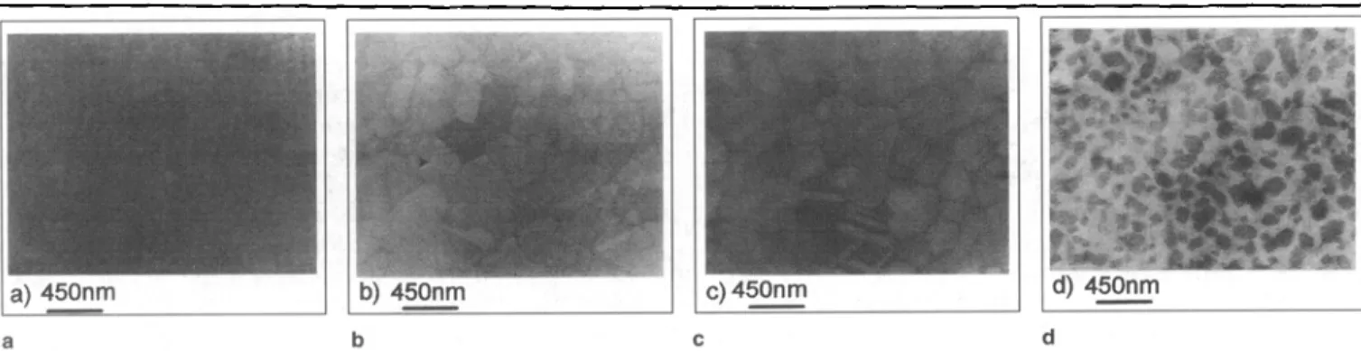
Fig. 4. Surface morphology of the Au/MoFli/Ge/Pd metallization samples rapid thermal annealed for 60 s at different annealing temperatures. (a) 350 (b) 450, (c) 475, and (d) 500~
Au/Ge/Pd Ohmic Contacts to n-GaAs with
the Mo/Ti Diffusion Barrier 1821
i ~ i o - . / \ z / / ,0 ~ ~ 9 ~ / o : I I i : / ~ : : ,= - - , , s - - x , , _ ' i -~ Y " ~ " - t , ... ... ::.. A,MMc.'Ti,'GeIPd/n~ (RTA~'Ct60~) ]
/
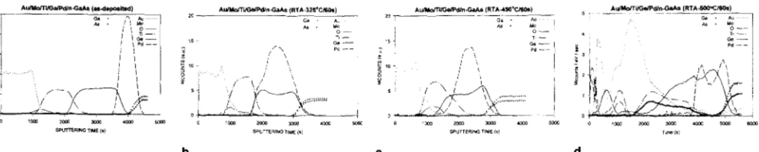
2 ~. J } i ? o 1 ~ c ~ o 0 ~ ~ o c ~ ~ x ~ a b c dFig. 5. AES depth profiles of each element for (a) the as-deposited Au/Mo/Ti/Ge/Pd/n-GaAs sample and those rapid thermal annealed for 60 s at the annealing temperatures of (b) 325, (c) 450, and (d) 500~
graphs are therefore shown. The micrographs for the samples annealed at 350, 450, and 475~ are shown in Figs. 4a-4c, respectively. The very smooth surface morphology is supposed to be due to the superior efficiency of the Mo/Ti-bilayer as the diffusion barrier for the As-outdiffiusion and Au-indiffiusion. Hence, the surface of the sample annealed at 500~ is still more or less smooth, as shown in Fig. 4d. F u r t h e r increase in the annealing t e m p e r a t u r e deteriorates the surface morphology of the samples.
Because of the significant influences of the dif- fusion barrier on the variations of the electrical char- acteristics and the surface morphologies with anneal- ing t e m p e r a t u r e described above, the As-outdiffusion and Au-indiffusion are therefore thought to be very important to the performances of ohmic contacts. Since m a n y tiny holes are observed in the Au/Ge/Pd samples even at the annealing t e m p e r a t u r e of 325~ and since the H 2 contained in the forming gas anneal- ing ambient is expected to easily carry As away, it is believed t h a t the higher p s for the Au/Ge/Pd samples without any diffusion barrier are caused by the As- outdiffusion, resulting in the deterioration of GaAs surface. Also, Au diffuses easily through the metallic overlayer to react with Ga and provide m a n y Ga vacancies for Ge-incorporations. The formation of Ga vacancies and the e n h a n c e m e n t of Ge-doping in GaAs then compensate the effects from the As-outdiffiusion, which are surmised to be responsible for the improve- m e n t of pcs to a lower value again. But, massive interactions between Au and the GaAs s u b s t r a t e s m as well as the persistent As-outdiffusion for even higher annealing t e m p e r a t u r e would destroy the active layer and thus result in the further degradation of pcs. By additionally depositing a Ti or Mo/Ti-bilayer, good diffusion barrier is provided. Because these two types of samples have similar electrical characteristics from 325 to 400~ it seems t h a t they do not differ signifi- cantly in the ability to prevent As-outdiffiusion. But the onset of the second lowering of pc for the Au/Ti/Ge/ Pd/GaAs samples occurs at 425~ which is signifi- cantly lower t h a n 500~ for the Au/Mo/Ti/Ge/Pd/ GaAs ones. This is due to the difference in the efficien- cies of retarding the Au-indiffusion by the Ti and Mo/ Ti-bilayer. The Au/Mo/Ti/Ge/Pd specimens possess the highest contact resistively at the 450~ annealing among these three types of samples, which is also attributed to the efficient retardation of the Au- indiffusion by the Mo/Ti-bilayer.
To further clarify the barrier effect of the Mo/Ti- bilayer on the As-outdiffusion and Au-indiffiusion, AES depth analysis is performed. The depth profile of each element for the as-deposited Au/Mo/Ti/Ge/Pd samples are shown in Fig. 5a. No obvious interaction among different layers is found. The TiO~ formed by the exposure to the oxygen after the deposition of Ti is observed at the interface between Mo and Ti where the tail of Au ends. In Fig. 5b, for the samples an- nealed at 325~ achieving low Pc, the distribution of As moves very slightly further toward the surface t h a n the Ga. But it seems t h a t the ohmic characteris- tics are not deteriorated. The distributions of Pd and Ge imply the formation of PdGe phase at the GaAs surface. This is consistent with previous investiga- tions 11-13 that the PdGe is essential to obtaining low pcs. The retardation of Au-indiffusion by the Mo/Ti- bilayer is obvious from the distribution of Au being restricted to behind the oxygen signal of the TiO x. This result is consistent with the previous model, s Since the solubility of Au is very low in bulk Mo, Au atoms can migrate into the Mo layer through the structural defects in the Mo film. When the Ti and Mo are continuously deposited in a good vacuum condi- tion, the Au can therefore get through the defects in the Mo-layer to the Mo/Ti interface. However, in the samples with Ti layer exposed to oxygen before the deposition of Mo, all the easy paths for diffusion are blocked by oxygen atoms resulting in the prevention of Au-indiffusion and As-outdiffusion. Hence, the Mo/ Ti layer as a very efficient diffusion barrier does contribute to the formation of excellent ohmic con- tacts. The AES profiles for the sample annealed at 450~ are shown in Fig. 5c. The distributions of Ga and As are the same as those annealed at 325~ Also the distribution of Au is still blocked by the TiOx, although the oxygen atoms have moved deeply into the Ti layer. The only significant difference is in the distributions of Pd and Ge. An abnormally high Ge- containing layer is obviously formed on the GaAs surface, which is correlated to the degradation ofp~. It is believed t h a t high doping concentrations of Ge in GaAs results in highly compensated material and in some cases even p-type material.l~,14 Hence, the Mo/Ti bilayer significantly resist the Au-indiffusion, lead- ing to the highly compensated layer. For the samples annealed at 500~ Au atoms eventually migrate through the metal layers into the GaAs. The in- diffusion of Au is expected to enhance the creation of
Ga vacancies and therefore assist the Ge-incorporation which is responsible for the lowering of pcs. Since the layered metal structure is destroyed by the indiffusion Au, the elements are found to mix with each other in a complicated w a y as shown in Fig. 5d. On the other hand, the significant outdiffusion of As is also ob- served to be deterred by the Mo/Ti barrier.
CONCLUSIONS
In summary, samples with three different types of metallization structures are adopted to u n d e r s t a n d the influences of barrier metals on the ohmic charac- teristics of Au/Ge/Pd/GaAs. For Au/Ge/Pd/GaAs samples without any diffusion barrier, the specific contact resistivities are r e m a r k a b l y higher t h a n those with barriers of Ti and Mo/Ti. In addition, a large n u m b e r of tiny holes are found for the Au/Ge/Pd specimens b u t not for the samples with Ti and Mo/Ti barriers. The barrier metals are therefore surmised to effectively reduce the As-outdiffusion during thermal annealing. Consequently, the Au/Mo/Ti/Ge/Pd and the Au/Ti/Ge/Pd specimens possess lower p s and b e t t e r t h e r m a l reliability. For the Au/Mo/Ti/Ge/Pd samples, minimum Pc as low as 2 • 10 -7 ~-cm 2 can be achieved at an annealing t e m p e r a t u r e of 375~ and the annealing t e m p e r a t u r e range for such low pc s can be extended to about 400~ Moreover, the efficient retardation of the Au-indiffusion by the Mo/Ti-bilayer clarified by the AES depth profile results in a turn- around phenomenon of the specific contact resistivity at the relatively high annealing t e m p e r a t u r e of -500~ Hence, the efficient diffusion barrier of Mo/Ti is proven to be very useful for Au/Ge/Pd/n-GaAs ohmic contacts.
ACKNOWLEDGMENTS
The research was supported in part by the Republic of China National Science Council (R.O.C. NSC) un- der the Contract No. NSC-84-2622-E009-012. Tech- nical supports from the National Nano-Device Labo- ratory ofRO.C. NSC and the Semiconductor Research Center (S.RC.) of National Chiao Tung University were also acknowledged.
REFERENCES
1. N. Braslau and J.B. Gunn and J.L. Staples, Solid-State Electron. 10, 38 (1967).
2. E.D. Marshall, W.X. Chen, C.S. Wu, S.S. Lau and T.F. Kuech,
Appl. Phys. Lett. 47, 298 (1985).
3. E.D. Marshall, C.S. Wu, C.S. Pal, D.M. Scott and S.S. Lau,
Thin Films: The Relationship of Structure to Properties, ed.
C.R. Aita and K S. Sree Harsha 47, 161 (Pittsburgh, PA: Mater. Res. Soc., 1985).
4. E.D. Marshall, B. Zhang, L.C. Wang, P.F. Jiao, W.X. Chen, T. Sawada, S.S. Lau, KL. Kavanagh and T.F. Kuech, J. Appl. Phys. 62, 942 (1987).
5. J.T. Lai and J.Y.M. Lee, Appl. Phys. Lett. 64, 306 (1994).
6. A. Paccagnella, L.C. Wang, C. Canali, G~ Castellaneta, M. Dapor, G. Donzelli, E. Zanoni and S.S. Lau, Thin Solid Films
187, 9 (1990).
7. W.C. Huang, T.F. Lei and C.L. Lee, J. Electron. Mater. 23,
397 (1994).
8. J.W. Mayer and S. S. Lau, Electronic Materials Science: For Integrated Circuits in Si and GaAs, Ch. 11,331 (Macmillan,
1990).
9. J.W. Wu, Ph.D. Thesis, National Chiao Tung University (1995).
10. R. Williams, Modern GaAs Processing Methods, (London:
Artech House, 1990).
11. W.Y. Han,Y. Lu, H.S. Lee, M.W. Cole, L.M. Casas, A. DeAnni, K.A. Jones and L.W. Yang, J. AppL Phys. 74, 1 (1993).
12. M.W. Cole, W.Y. Hane, L.M. Casas, D.W. Eckart and K.A. Jones, J. Vac. Sci. Technol. A 12, 1904 (1994).
13. C.J. Palmstrom,S.A. Schwarz, E~ Yablonovitch, J.P.Harbison,
C.L. Schwartz, L.T. Florez, T.J. Gmitter, E.D. Marshall and S.S. Lau, J. Appl. Phys. 67, 1 (1990).