Bias-enhanced nucleation of oriented diamonds on cone-like Si
Li Chang
⁎
, Jhih-Kun Yan
Department of Materials Science and Engineering, National Chiao Tung University, Hsinchu, Taiwan Available online 14 January 2008
Abstract
Uniform distribution of bias-enhanced nucleation of diamond has been improved on Si substrate of an area of 1 × 1 cm2by using a dome-shaped Mo counter electrode in a microwave plasma chemical vapor deposition reactor. A nucleation density of 109cm2can be reached within a
few minutes when the bias voltage of−100 V is applied on the substrates. Scanning electron microscopy (SEM) and transmission electron microscopy (TEM) show that a single-crystalline diamond in a few nanometered size can be deposited on a volcano-shaped cubic SiC which is epitaxially formed on a Si cone. Examination reveals a large fraction of diamond nuclei are oriented along with one side of SiC on each Si cone. The Si cone formed on the Si substrate is due to plasma etching. The diamond nuclei have a shape close to rhombus in TEM. With further growth, secondary nucleation of diamond occurs on top of diamond nuclei and SiC which grows with Si cones. As a result, polycrystalline diamonds are deposited on each Si cone.
© 2008 Elsevier B.V. All rights reserved.
Keywords: Nucleation; Orientation; Bias; Microscopy
1. Introduction
Nanocrystalline diamond has many outstanding properties such as low optical absorption coefficient, good field emission efficiency, and good adhesion to substrates[1–5], so it has great potentials for applications in optical, electronic, and mechanical devices. Recently, chemical vapor deposition (CVD) method has been widely used to synthesize nanocrystalline diamonds, however, the diamonds usually appear as disordered crystals or in cauliflower-like shape in the film structure of diamond, which comprises high defect densities such as grain boundaries, stacking faults and five-fold twins [4,6–8]. Nanocrystalline diamond exhibiting regular shape with low defect density is rarely reported. Though bias-enhanced nucleation (BEN) of diamond has been extensively studied for more than a decade because of the possibility to deposit epitaxial diamond films, many issues still remain unresolved since the first report of BEN for diamond study by Yugo et al. [9, and for the details of recent review see reference 10]. In our previous studies, oriented diamonds in nanometer size can be deposited in a short bias time with a
designed Mo anode which improves the distribution of microwave plasma and dc glow discharge to obtain uniform diamond deposits[11,12]. It thus allows us systematic study of structural evolution of the nucleation and growth of diamond. The result have shown that there is a high density of cone-like particles uniformly deposited on the surface of the substrate and the structure of particles consists of a volcano shaped Si cone covered with epitaxial cubic SiC of which is topped with diamond. In the present paper, we used a patterned structure of SiO2on Si substrate to demonstrate the formation process of Si cones which helps to understand the mechanism for the formation of oriented diamonds during the bias stage. Also,
Diamond & Related Materials 17 (2008) 467–471
www.elsevier.com/locate/diamond
⁎ Corresponding author.
E-mail address:[email protected](L. Chang).
Table 1
Experimental deposition parameters for diamond nucleation Heating Bias
Power, W 800 800
Pressure, Torr 20 20
CH4in H2,% 2 5
Bias voltage on anode, V 0 100
Flow rate, sccm 300 300
Duration, min 10 1 (Sample A)
2 (Sample B, SiO2pattern)
4 (Sample C) 0925-9635/$ - see front matter © 2008 Elsevier B.V. All rights reserved.
the evolution of oriented diamond is discussed, based on the observation of electron microscopy.
2. Experimental
The nucleation of diamond was carried out in a 2.45-GHz ASTeX microwave plasma CVD reactor. For optimization of the microwave discharge and the extension of the bias discharge over the whole substrate, a dome-shaped Mo anode with a diameter of 15 mm was located above the substrate as counter-electrode. The distance between the anode and substrates was
varied in the range from 15 to 30 mm. The schematic diagram of the instrument has been described elsewhere[12].
The substrates were mirror-polished p-type (100) silicon wafers with dimension of 1 × 1 cm2 without any mechanical pretreatment. Before loading into the reactor, the substrate was etched in 1% hydrofluoric acid in de-ionized water for 60 s to remove native oxide on Si, and ultrasonically cleaned with acetone for 10 min. The substrate was then placed on a Mo disk holder in the reactor.
A hydrogen plasma with addition of 2% CH4concentration was initially applied to the substrate for 10 min for heating to the required temperature (about 800 °C) as measured by an optical pyrometer and to remove any residual of native oxide on Si surface, followed by applying a bias voltage of +100 V on the Mo anode for different bias time with 5% methane concentra-tion. During the bias, the substrate temperature was about 850 °C. The detailed process parameters are listed inTable 1. Samples obtained by biasing with 1 min, 2 min (patterned sample) and 4 min are designated as A, B and C, respectively. After the bias process, the surface morphologies and micro-structures were examined using a JEOL JSM-6700F field-emission scanning electron microscope (SEM) and a Philips Tecnai 20 transmission electron microscope (TEM).
3. Results and discussion
Experimental observations have shown that the nucleation density of diamond is generally increased with the bias voltage
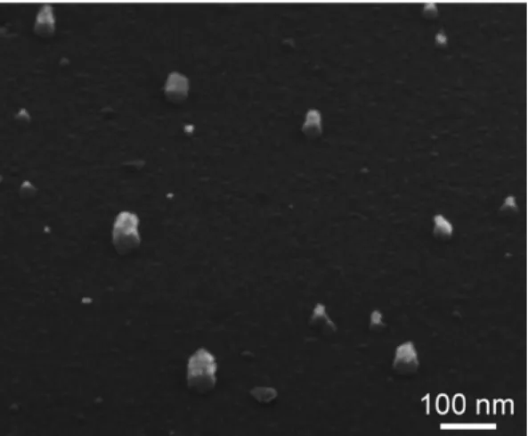
Fig. 1. SEM micrograph of Sample A synthesized at 100 V bias with 5% CH4
concentration for 1 min.
Fig. 2. (a) Cross-sectional bright-field TEM of Sample A showing the diamond nuclei on Si (100) substrate, (b) and (c) Enlarged images from framed region in (a) with the corresponding electron diffraction patterns in (d) and (e) along Si[110] direction, respectively. Solid lines in (d) and (e) showing SiC pattern, and dotted lines diamond pattern.
and CH4 concentration [13]. In the following, we show the results obtained from sample deposited with 100 V and 5% CH4.
Fig. 1shows the surface morphology of Sample A after the bias stage for 1 min. The deposits on the substrate surface exhibit a cone-like shape, and the estimated density of the deposited particles is about 4 × 109cm− 2. It is interesting to see that there is almost a single bright crystallite on the small cones, and on larger cones there are a number of polycrystallites. These crystallites are actually diamond as shown by TEM.Fig. 2(a) is a typical bright-field TEM micrograph of Sample A in cross-section view of the deposited crystals on the Si substrate. The rhombus-like diamond crystals with facets can be clearly seen on top of the Si cones which exhibit dark contrast. All diamond particles were formed only on the Si cones, not on flat Si substrate surface. The height of the Si cones is about 6–8 nm.
Between diamond and Si is the SiC in grey contrast. The image shows that the cone structures in SEM consist of diamond, SiC and Si. As shown in Fig. 2(b) and (c) of the corresponding selected-area diffraction (SAD) patterns along Si [011] zone-axis from the left-hand side (region 1) and right-hand side (region 2), respectively, the SiC and diamond reflections can be indexed as b110N axis pattern, and exhibit single crystalline characteristics. Furthermore, the SiC and Si reflections shows that all SiC are in epitaxy with Si, and the diamond on the left hand side has {111} plane parallel to {111} of SiC, while the right-side diamond is deviated a few degrees from SiC {111}. However, both diamonds have b110N parallel to those of SiC and Si, and probably have {111} facets. Therefore, the diamonds are oriented with respect to Si. The more detailed description for TEM characterization can be found in the reference [10]. From high-resolution TEM observation (not
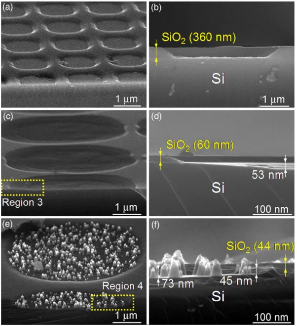
Fig. 3. SEM images of Sample B on patterned Si substrate with SiO2. (a) tilt, and (b) cross-section view of SiO2pattern, (c) surface morphology after the heating
shown), the epitaxial SiC grows on the sides of Si cones which results in the formation of volcano-type holes. It has been suggested that volcano SiC provides the nucleation site for oriented diamonds.
Although the nucleation mechanism of diamond on Si (100) in the early stage of biasing has been realized, the reason for the formation of the Si cone is not well understood. The formation process of Si cone can be demonstrated by using a patterned structure of SiO2on Si substrate (Sample B). InFig. 3(a), the SEM image shows a tilt view of the patterned sample and the size of the hole is about 3.7μm in diameter.Fig. 3(b) is a cross-sectional view of the sample showing that the interface between SiO2and Si substrate is smooth and the thickness of SiO2layer is about 360 nm.Fig. 3(c) displays the morphology after 10 min heating process, the diameter of the hole is enlarged to about 4.3μm and the Si substrate with SiO2pattern can be still seen. An enlarged view of Region 3 ofFig. 3(c) is displayed inFig. 3
(d) which reveals the interface of SiO2with Si substrate. Based on the position of the interface between SiO2and Si substrate as reference which was not affected by the plasma etching, we can measure that the thickness of SiO2 layer was reduced from 360 nm to 60 nm. In the center of holes, the Si substrate was etched away about 53 nm in depth. After the heating and 2 min bias process, Fig. 3(e) shows that there are many cone-like particles topped with diamond nanocrystallites within the holes, and the SiO2layer is still survived. From the reference position of the interface between SiO2and Si substrate, the thickness of
SiO2layer is measured to be reduced from 60 nm to 44 nm, and the Si substrate at the center of the hole has a depth of about 73 nm as shown inFig. 3(f) of an enlarged view of Region 4 in
Fig. 3(e). In particular, some cone-like particles are higher than the interface between SiO2and Si substrate, suggesting that Si cones grow with bias time. Compared with the TEM result (Fig. 2), the average height of Si cones is about one-third or less of the height of cone-like structure, so the reasonable explanation for the formation of Si cone may be due to the etching of Si substrate by the plasma in bias stage.
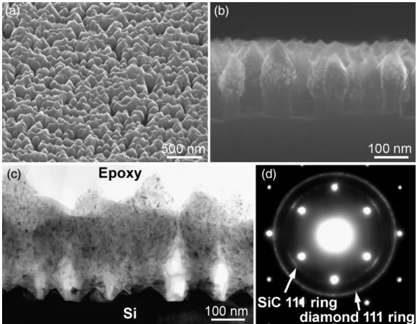
After longer bias application for 4 min, the surface morphology of sample C is shown inFig. 4(a). The density of deposits estimated from SEM is slightly increased to about 6.7 × 109 cm− 2. The image also shows that the particles are already connected to each other after this bias time. The cross-sectional view inFig. 4(b) shows the height of tree-like particles in the range of 300–350 nm with an average of ~335 nm. Also, the appearance shows that top region of the particles is composed of multi-granular diamond, while the half bottom is cylinder shape instead of cone-like one. To realize the formation of the tree-like particles, further TEM characterization was carried out. A typical bright-field TEM micrograph in cross-sectional view shown inFig. 4(c) reveals the tree-like structure with many diamond crystallites in nanometer size on the top half of the trees similar to the SEM observation in Fig. 4(b).
Fig. 4(d) is the corresponding selected-area electron diffraction pattern along Si [011] zone-axis in which diamond {111} and
Fig. 4. Sample C synthesized with 5% CH4concentration for 4 min. (a) SEM micrograph, (b) SEM micrograph in cross-section, (c) bright-field TEM image of tree-like
cubic SiC {111} rings can be identified. This sample has a strong texture for SiC as evidenced by arc regions of strong intensity along the (111) SiC ring which appear in registry with silicon {111} spots. However, there are a large fraction of disoriented SiC crystals as shown by the continuous rings in the diffraction pattern. The SiC also grows with bias time, resulting from reaction of carbon with silicon in the vicinity of vapor phase due to etching. For deposited diamonds, the diamond {111} ring of uniform intensity distribution suggests that diamond nanocrystallites are randomly oriented. The random orientations of diamond particles are likely due to secondary nucleation and gradually disordered SiC. When more diamonds cover on top of a Si cone, they act as the shield for the underneath Si. As a result, the Si cone gradually changes the morphology to cylinder shape for the bottom half. With growth of diamond to the extent of contact with each other, Si may be prevented from further etching by the shield of continuous diamond film, and it stops further deposition of SiC.
From the above results which clearly show the role of Si substrate on the evolution of diamond nucleation process, oriented diamonds can be formed on small Si cones through epitaxial SiC in the early stage of biasing, and formation of polycrystalline diamonds occurs in the later stage due to further Si etching which assists more SiC deposited in misorientation. It has been pointed out that etching of Si substrate occurs in the bias stage by Yugo et al.[9]. The present evidence clearly shows that etching of the silicon substrate progresses during biasing if the surface has not been covered with a continuous film. It is expected in the future that a more delicate bias processing in short bias-enhanced nucleation followed by growth without bias
or with reduction of Si etching and dilute CH4concentration in the later stage should be applied for improvement of oriented diamond in film growth. In addition, control of oriented nucleation of diamond can be helpful to obtain new nanos-tructural diamond films.
Acknowledgements
This work was supported by the National Science Council, Taiwan, R.O.C. under contract of NSC 95-2221-E-009-089-MY3. References
[1] D.M. Gruen, S. Liu, A.R. Krauss, J. Luo, X. Pan, Appl. Phys. Lett. 64 (1994) 1502.
[2] D.M. Gruen, S. Liu, A.R. Krauss, X. Pan, J. Appl. Phys. 75 (1994) 1758. [3] S.G. Wang, Q. Zhang, S.F. Yoon, J. Ahn, Q. Wang, D.J. Yang, Q. Zhou, Q.F.
Huang, Mater. Lett. 56 (2002) 948.
[4] X. Jiang, C.L. Jia, Appl. Phys. Lett. 80 (2002) 2269.
[5] M.Q. Ding, W.B. Choi, A.F. Myers, A.K. Sharma, J. Narayan, J.J. Cuomo, J.J. Hren, Surf. Coat. Technol. 672 (1997) 94.
[6] X.T. Zhou, Q. Li, F.Y. Meng, I. Bello, C.S. Lee, S.T. Lee, Y. Liftshitz, Appl. Phys. Lett. 80 (2002) 3307.
[7] D. Shechtman, A. Feldman, M.D. Vaudin, J.H. Hutchison, Appl. Phys. Lett. 62 (1993) 487.
[8] D. Dorignac, V. Serin, S. Delclos, F. Phillipp, D. Rats, L. Vandenbulcke, Diamond Relat. Mater. 6 (1997) 758.
[9] S. Yugo, T. Kanai, T. Kimura, T. Muto, Appl. Phys. Lett. 58 (1991) 1036. [10] K. Kobashi, Diamond Films– Chemical Vapor Deposition for Oriented
and Heteroepitaxial Growth, Elsevier, Amsterdam, 2005. [11] J.K. Yan, L. Chang, Nanotechnology 17 (2006) 5544. [12] J.K. Yan, L. Chang, Thin Solid Films 498 (2006) 230. [13] J.K. Yan, PhD Thesis, National Chiao Tung University, (2006).