Strain relaxation in In As In Ga As quantum dots investigated by photoluminescence
and capacitance-voltage profiling
J. F. Chen, R. S. Hsiao, Y. P. Chen, J. S. Wang, and J. Y. Chi
Citation: Applied Physics Letters 87, 141911 (2005); doi: 10.1063/1.2081132
View online: http://dx.doi.org/10.1063/1.2081132
View Table of Contents: http://scitation.aip.org/content/aip/journal/apl/87/14?ver=pdfcov Published by the AIP Publishing
Articles you may be interested in
Photoluminescence characteristics of InAs self-assembled quantum dots in In Ga As Ga As quantum well J. Appl. Phys. 101, 126101 (2007); 10.1063/1.2745410
Quantum dot strain engineering of In As In Ga As nanostructures J. Appl. Phys. 101, 024313 (2007); 10.1063/1.2424523
Temperature dependence of the photoluminescence properties of self-assembled In Ga As Ga As single quantum dot
J. Appl. Phys. 100, 103515 (2006); 10.1063/1.2387054
1.55 m emission from In As Ga As quantum dots grown by metal organic chemical vapor deposition via antimony incorporation
Appl. Phys. Lett. 89, 083116 (2006); 10.1063/1.2337163
Effects of rapid thermal annealing on device characteristics of In Ga As Ga As quantum dot infrared photodetectors
J. Appl. Phys. 99, 114517 (2006); 10.1063/1.2202704
This article is copyrighted as indicated in the article. Reuse of AIP content is subject to the terms at: http://scitation.aip.org/termsconditions. Downloaded to IP: 140.113.38.11 On: Thu, 01 May 2014 02:47:51
Strain relaxation in InAs/ InGaAs quantum dots investigated by
photoluminescence and capacitance-voltage profiling
J. F. Chen, R. S. Hsiao, and Y. P. Chen
Department of Electrophysics, National Chiao Tung University, Hsinchu, Taiwan, Republic of China
J. S. Wang
Department of Physics, Chung Yuan Christian University, Chung-Li, Taiwan, Republic of China
J. Y. Chi
Industrial Technology Research Institute (OES/ITRI), Hsinchu, Taiwan, Republic of China
共Received 30 March 2005; accepted 9 August 2005; published online 29 September 2005兲 We present detailed studies of the onset of strain relaxation in InAs/ InGaAs quantum dots. We show that the ground-state photoluminescence共PL兲 emission redshifts with increasing the InAs coverage before relaxation and blueshifts when relaxation occurs. PL spectra of the relaxed samples show two predominant families of dots with very different temperature-dependent efficiency. By comparison we show that the dots emitting at long wavelength are degraded by relaxation while the dots emitting at short wavelength remain coherently strained. Consequently, the PL spectra are dominated by the dots emitting at short wavelength, leading to the observed blueshift. This result suggests that the relaxation does not occur uniformly. In addition, we show that the relaxation occurs in the dot bottom interface. © 2005 American Institute of Physics. 关DOI:10.1063/1.2081132兴
The InAs/ GaAs self-assembled quantum dots 共QDs兲 共Refs. 1–5兲 have attracted considerable attention for their promising technological applications.6–8Increasing the InAs coverage can increase the dot size. However, when the InAs coverage is increased beyond a critical thickness, strain relaxation9in the QD occurs. Local strain has been shown to alter the properties of the QD. Strain-induced intermixing10 and In segregation11has been reported. However, the experi-mental data concerning the effect of relaxation on the size distribution of the dots and their properties have seldom been reported. We have previously characterized the strain relax-ation in InAs QD capped with GaAs 共Ref. 9兲 and found complete carrier depletion in the QD. Capping the QD with an InGaAs layer has been shown to reduce the strain and achieve an emission at over 1.5m.12 This strain-reducing InGaAs layer is expected to influence the relaxation process. Therefore, in this work, we have capped the InAs dots with an InGaAs layer and investigated the strain relaxation by carefully increasing the InAs coverage thickness.
The QD structures were grown on n+-GaAs 共100兲 sub-strates by solid source molecular beam epitaxy in a Riber Epineat machine. On top of a 0.2m-thick Si-doped GaAs 共6–10⫻1016cm−3兲 barrier layer, an InAs layer with different
thickness from 1.97 to 3.33 ML was deposited at 490°C to form the QDs. Then the QDs were capped with a 60 Å In0.15Ga0.85As layer and a 0.2m-thick Si-doped GaAs
共6–10⫻1016cm−3兲 barrier layer to finish the growth. Detail
growth conditions can be found elsewhere.13 A QD sheet density about 3⫻1010cm−2 was observed by atomic field
microscopy共AFM兲 images. For capacitance-voltage 共C−V兲 profiling, Schottky diodes were realized by evaporating Al on the sample. PL measurements were carried out using a double frequency yttrium-aluminum-garnet共YAG兲: Nd laser at 532 nm.
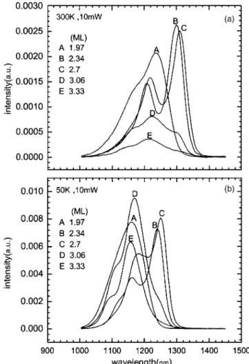
Figures 1共a兲 and 1共b兲 show the 300- and 50-K PL spectra for different InAs coverage of 1.97, 2.34, 2.7, 3.06, and 3.33 ML. The laser power was kept at 10 mW for all samples. A
redshift of the ground-state emission from 1238 to 1300 and to 1310 nm can be seen as the InAs coverage is increased from 1.97 to 2.34 and to 2.7 ML. This redshift was previ-ously observed and explained by an increase in the dots size.14 DLTS measurement shows no trapping signals in these samples, indicating coherent QD formation. However, as the InAs coverage is increases to 3.06 ML, the ground-state peak is blueshifted to 1223 nm accompanied with broadening spectra. Further increasing the InAs coverage to 3.33 ML, the peak is further blueshifted to 1215 nm. This sudden blueshift and linewidth broadening are indicative of strain relaxation. Consequently, the InAs critical thickness for the relaxation shall be between 2.7 and 3.06 ML.
Detailed examination of the PL spectra shows the pres-ence of two predominant families of dots in the relaxed samples. In the 3.06 ML coverage, besides the dots emitting at 1223 nm, another family of dots emitting at about 1300 nm can be seen in Fig. 1共a兲, suggesting that the relaxation does not occur uniformly. From their excitation power de-pendence, the possibility that these two peaks are related by ground and excited state is excluded. The dots emitting at 1300 nm are relatively weak in intensity. Figure 2 shows the temperature-dependent PL spectra of this sample. The two families of the dots show very different temperature depen-dence of the radiation efficiency. At 300 K, the peak intensity of the dots emitting at 1223 nm is only slightly stronger than that of the dots emitting at 1330 nm. However, as tempera-ture decreases to 50 K, the peak intensity at 1223 nm in-creases in efficiency by a factor of 10 as compared to only 2 for the peak at 1300 nm, indicating that the dots emitting at 1300 nm are degraded by relaxation defects through which carriers are recombined. By comparison, the dots emitting at 1223 nm are not degraded by relaxation because its intensity is even stronger than that of the nonrelaxed dots emitting at 1238 nm in the 1.97 ML coverage at low temperatures as shown in Fig. 1共b兲, suggesting that the dots emitting at 1223 nm are still coherently strained. Consequently, the PL spectra
APPLIED PHYSICS LETTERS 87, 141911共2005兲
0003-6951/2005/87共14兲/141911/3/$22.50 87, 141911-1 © 2005 American Institute of Physics This article is copyrighted as indicated in the article. Reuse of AIP content is subject to the terms at: http://scitation.aip.org/termsconditions. Downloaded to IP:
are dominated by the dots emitting at 1223 nm, explaining the observed blueshift. The 3.33-ML sample shows similar two predominant families of dots emitting at 1215 and 1300 nm, respectively. The peak around 1300 nm is weaker than that of the 3.06 ML sample, consistent with a larger degree of relaxation.
Figure 3 shows the temperature dependence of the full-width at half-maximum共FWHM兲 of the ground-state peaks for the samples. The 1.98 ML coverage has the largest low-temperature FWHM 共⬃70 meV兲, reflecting the inhomoge-neous distribution of dots size. When temperature is in-creased, the FWHM decreases gradually for temperatures higher than 150 K. A fast redshift of the peak energy is accompanied with this reduction of FHWM. This behavior has been previously reported15and explained by the transfer of electrons from small to large dots that have confined states at lower energies. When InAs coverage is increases to 2.34 and 2.7 ML, FWHM decreases to about 35–40 meV, due to improved size homogeneity for large dots.14When tempera-ture is increased, the effect for the electron transfer is less apparent and the FWHM is nearly invariable. Relaxation leads to a large FWHM about 60–67 meV共at 50 K兲 for the 3.06 and 3.33 ML coverage. These samples contain two families of dots. The FWHM shown here is obtained from the dots emitting at shorter wavelength. Since these dots are coherently strained, probably due to better size homogeneity,
the low-temperature FWHM is narrower than that of the non-relaxed 1.98 ML. When temperature is increased, the elec-trons transfer from the dots emitting at 1223 nm to the dots emitting at 1300 nm, leading to a rapid decrease in the in-tensity and increase in the FWHM of the peak at 1233 nm for temperatures higher than 200 K. This trend is even more pronounced in the 3.33 ML, where the FWHM rapidly in-creases with increasing temperature higher than 150 K.
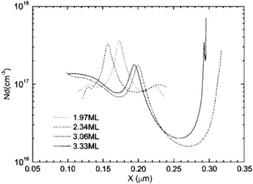
Figure 4 shows the 300-K concentration profiles at 1 MHz for the different InAs coverage. It can be seen that the non-relaxed samples show a strong accumulation peak in the dots and symmetric depletion on both sides. In contrast, the relaxed samples show a relatively weak peak with drastic depletion in the neighboring bottom GaAs layer. This carrier depletion must be induced by relaxation by producing defect traps which were previously reported to be acceptorlike.9,16 The irregular heavy doping around 0.3m provides the evi-dence of the presence of the relaxation traps in the depletion region. Due to a long emission time, the electrons that cannot follow ac signal to emit out of the traps will be swept out
FIG. 1.共a兲 300 K PL spectra for InAs coverage of 1.97, 2.34, 2.7, 3.06, and 3.33 ML, showing a redshift from 1238 to 1310 nm with increasing the InAs coverage from 1.97 to 2.7 ML and a blueshift as the InAs coverage is increased to 3.06 and 3.33 ML.共b兲 The corresponding PL spectra at 50 K.
FIG. 2. Temperature-dependent PL spectra for the 3.06 ML InAs coverage, showing two predominant families of dots emitting at 1223 and 1300 nm共at 300 K兲, respectively. While their peak intensities are nearly comparable at 300 K, as temperature decreases to 50 K, the peak intensity at 1223 nm increases in efficiency by a factor of 10 as compared to only 2 for the peak at 1300 nm, suggesting that the dots emitting at 1300 nm are degraded by relaxation.
FIG. 3. Temperature dependence of the FWHM of the ground-state peaks for different InAs coverage. In the 3.06 and 3.33 ML samples, the FWHM is obtained from the dominant peaks at 1223 and 1215 nm, respectively. 141911-2 Chen et al. Appl. Phys. Lett. 87, 141911共2005兲
This article is copyrighted as indicated in the article. Reuse of AIP content is subject to the terms at: http://scitation.aip.org/termsconditions. Downloaded to IP: 140.113.38.11 On: Thu, 01 May 2014 02:47:51
when dc bias shifts Fermi level well below the traps level. Deep-level transient spectroscopy 共DLTS兲 spectra reveal a broad trap at 0.37 and 0.41 eV共with capture cross sections of 5.45⫻10−17and 9.78⫻10−16cm2兲 for the 3.06 and 3.33 ML
coverage, respectively. We detect no traps in the top GaAs layer. Consequently, this trap is the relaxation trap that causes the carrier depletion. This result shows that the large strain induced in the bottom interface by the evolving dots is relieved by the formation of this defect trap. Given the dot size fluctuation, a certain degree of spatial randomness sets in, thus giving rise to the nonuniform strain relaxation ob-served in the PL data. Our results demonstrate the important role of the evolving strain fields16 as a source of driving force for self-assembled growth, consistent with a phenom-enological model proposed by Xie et al.17 In terms of its Arrhenius plots, the trap detected here is similar to the trap observed in relaxed InGaAs/ GaAs quantum-well structures and shall be related to the relaxation-induced dislocations.18 The fact that the bottom GaAs layer is depleted by re-laxation is different from what we observed previously in relaxed InAs dots without the InGaAs cap layer,9 in which we observed complete carrier depletion in the dots and both the neighboring GaAs layers. We found that, by adding the InGaAs layer, together with a careful control of the InAs coverage, the relaxation-induced depletion can occur only in
the bottom GaAs layer and the QD region still contains free electrons. This result shows that the InGaAs layer has the effect of alleviating the strain12in the top GaAs layer and, as a result, the top GaAs layer remains strained. Since the depletion is caused by relaxation, the fact that the depletion only in the bottom GaAs layer strongly suggests that the relaxation occurs in the QD bottom interface. Similar relax-ation has been observed in GaAs/ InGaAs quantum well structures,19in which the relaxation takes place in the bottom interface while the top interface still remains strained.
The authors would like to thank the National Science Council of the Republic of China, Taiwan for financially sup-porting this research under Contract No. NSC-93-2112-M-009-002.
1F. Heinrichsdorff, M.-H. Mao, N. Kirstaedter, A. Krost, and D. Bimberg, Appl. Phys. Lett. 71, 22共1997兲.
2D. J. Eaglesham and M. Cerullo, Phys. Rev. Lett. 64, 1943共1990兲. 3D. Leonard, K. Pond, and P. M. Petroff, Phys. Rev. B 50, 11683共1994兲. 4J. M. Moison, F. Houzay, F. Barthe, and L. Leprince, Appl. Phys. Lett. 64,
196共1994兲.
5C. W. Snyder, J. F. Mansfield, and B. G. Orr, Phys. Rev. B 46, 9551 共1992兲.
6H. Shoji, K. Mukai, N. Ohtsuka, M. Sugawara, T. Uchida, and H. Ish-ikawa, IEEE Photonics Technol. Lett. 7, 1385共1995兲.
7G. Yusa and H. Sakaki, Electron. Lett. 32, 491共1996兲.
8J. C. Campbell, D. L. Huffaker, H. Deng, and D. G. Deppe, Electron. Lett. 33, 1337共1997兲.
9J. S. Wang, J. F. Chen, J. L. Huang, P. Y. Wang, and X. J. Guo, Appl. Phys. Lett. 77, 3027共2000兲.
10M. O. Lipinski, H. Schuler, O. G. Schmidt, K. Eberl, and N. Y. Jin-Phillipp, Appl. Phys. Lett. 77, 1789共2000兲.
11J. G. Garcia, J. P. Silveira, and F. Briones, Appl. Phys. Lett. 77, 409 共2000兲.
12J. Tatebayashi, M. Nishioka, and Y. Arakawa, Appl. Phys. Lett. 78, 3469 共2001兲.
13J. F. Chen, R. S. Hsiao, S. H. Shih, P. Y. Wang, J. S. Wang, and J. Y. Chi, Jpn. J. Appl. Phys., Part 1 43, L1150共2004兲.
14J. Tersoff, C. Teichert, and M. G. Lagally, Phys. Rev. Lett. 76, 1675 共1996兲.
15L. Brusaferri, S. Sanguinetti, E. Grill, M. Guzzi, A. Bignazzi, F. Bogani, L. Carraresi, M. Colocci, A. Bosacchi, P. Frigeri, and S. Franchi, Appl. Phys. Lett. 69, 3354共1996兲.
16S. S. Li, J. B. Xia, Z. L. Yuan, Z. Y. Xu, W. Ge, X. R. Wang, Y. Wang, J. Wang, and L. L. Chang, Phys. Rev. B 54, 11575共1996兲.
17Q. Xie, A. Madhukar, P. Chen, and N. P. Kobayashi, Phys. Rev. Lett. 75, 2542共1995兲.
18J. F. Chen, P. Y. Wang, J. S. Wang, C. Y. Tsai, and N. C. Chen, J. Appl. Phys. 87, 1369共2000兲.
19J. F. Chen, P. Y. Wang, J. S. Wang, N. C. Chen, X. J. Guo, and Y. F. Chen, J. Appl. Phys. 83, 1251共2000兲.
FIG. 4. 300-K concentration profiles measured at 1 MHz for different InAs coverage of 1.97, 2.34, 3.06, and 3.33 ML. The relaxed 3.06 and 3.33 ML samples show a relatively weak accumulation peak in the dots and drastic depletion in the bottom GaAs layer.
141911-3 Chen et al. Appl. Phys. Lett. 87, 141911共2005兲
This article is copyrighted as indicated in the article. Reuse of AIP content is subject to the terms at: http://scitation.aip.org/termsconditions. Downloaded to IP: 140.113.38.11 On: Thu, 01 May 2014 02:47:51