VLSl
design
for high-speed
LZ-based data
compression
J.-M.Chen and C.-H.Wei
Abstract: A simple real-time parallel architecture for CMOS VLSI implementation of a Ziv-hmpel data compression system is presented. This encoding system employs a linear systolic array to find concurrently the matches between each input data character and its corresponding dictionary, and can easily achieve ideal compression ratio by cascading the chips of the encoding cell. A new encoding architecture is proposed to improve the encoding speed and reduce hardware complexity for the encoding cells. In addition, the number of memory accesses is reduced to save power consumption for high-speed applications. T h e encoder codes one character (more than eight bits) per encoding cycle. The clock rate by Verilog simulator can be constrained below lSns using the Compass standard cell library for the 0 . 6 ~ CMOS process.
1 Introduction
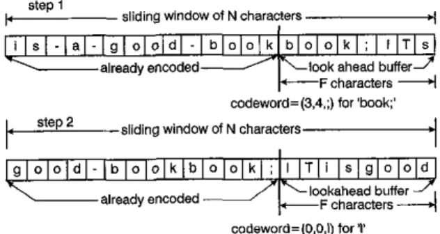
In recent years the need to develop efficient data compres- sion methods has increased considerably owing to the iucreasing applications of data compression in various areas. The most widely used classes of lossless data com- pression algorithms are those developed by Ziv and Lempel in 1977 and 1978, labelled as LZ77 and LZ78, respectively [l, 21. In the LZ77 algorithm, pointers are used to denote phrases in a fixed-size window that precedes the coding position, There is a maximum length for substrings that may be replaced by a pointer, given by the parameter F
(typically 24-25). These restrictions allow LZ77 to be imple- mented using a 'sliding window' of N characters. In this scheme the first N - F characteis have already been
encoded and the last F characters constitute a lookahead
buffer. The window is illustrated in example 1 (see Fig. 1).
step 1
k
- sliding window of N characters 4 -I
l g l o l o i d l
- 1
b l o l o l k l b l o l o l k l ;I
IlTlsalready encoded- look ahead buffer Fcharacters 4
codeword=(3,4,:) for 'book p-siiding window of N characters
,
,
g l o l o l d l - ) b l o l o l k ) b l o l o l k / ; I i I T l i l s l g l o l o l d already encoded
2
L F c h a m c t e r s A lookahahead buffercadeword=(0.0.1) for r'
Fig. 1 Imphemxion ofLZ77 dgorirhm urhg slidffl~ ~'iwfoiv of N &mac
To encode a character, the frst N - F characters of the
window are searched to find the longest match with lookahead buffer. The match may overlap with the buffer but obviously cannot be the buffer itself. The longest match is then encoded into a triple codeword (0, l, U ) where o is
IerS
0 IEE, 1999
IEE Proceedfflgs o&e no. 19990535
DOL 10.1049/ipcds:19990535
Paper fust r e c e i v e d 16th January 1998 and in re<& fonn 26th March 1999 The authors are with the Lkpamnent of Electronics En&eering, National
Chiao Tung University, m c h u , Taiwan, Republic of China
268
the offset of the longest match from the lookahead buffer, 1
is the longest length of match, and a is the first character that did not match the substring in the window. The win- dow is then shifted right I
+
1 characters, ready for the next encoding step. Attaching the explicit character to each pointer ensures that coding can proceed even if no match is found for the first character of the lookahead buffer.In the LZ77 algorithm, whenever there is no match or if there is a match of length one, each symbol that r e s p tively constitutes the matched substrings would be substi- tuted by a codeword of three bytes long. This may result in expansion rather than compression in the encoding process. If many such unfavourable codewords occurred in a file, the compression achieved would be low. The LZSS algo- rithm [3], one of the variants of the LZ77 algorithm, adopts a free mixture of pointer and characters to replace the triple codeword in LZ77 [l] to overcome the expansion problem. A character itself will be used only when a pointer takes more space than the characters it encodes. An extra bit, known asflug, is added to each pointer or character to dis- tinguish between them. The output is packed so that there are no unused bits. Many designers have incorporated this technique in the software implementation which signifi- cantly improves the compression ratio. However, the speed of data compression by software is usually not satisfactory for a real-time system.
Several LZ hardware architectures have been presented in the literature
[ H I .
The most computationally expensive step in the hardware is to search for the maximum match- ing strings in the sliding dictionary. However, the LZ-based algorithm must be executed at a very high throughput rate for real-time transmission and storage. The content addressable memory (CAM) approach [7] can provide con- stant time to search the matching strings for each symbol, but it must consume static DC current for many of the CAM cells during the match action cycle. If the size of the sliding window is increased the power consumption prob- lem will dominate the chip performance.We present the design of a systolic array processor for efficient implementation of the LZSS compression tech- nique by using wrap architecture [9]. This new approach can fmd a maximum match length for each clock cycle. The new hardware structure can execute the data compres- sion task on-thefly in the real-time communication system.
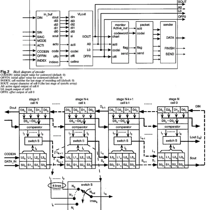
Fig.2 Bcock&grm ofencoder
CODEIN: initial iength value for codeword (default: 0) OFFIN initial ofiset value for codeword (defalt: 0)
INDEX. cell number for l a ? stage of e n d i n g cell (default: 0) SOW: output character of cell 0 (the last stage of ~ystolic a m y )
A 0 active signal output of cell 0
Lo: length oulpul of cell 0
OFF0 ojj..er output of cell 0
Fig. 3 A m y dalafrow of w o p architecture for mmditg systm
To implement the encoder with VLSI ASIC dsign tech- nology, the system is divided into several modules and facilitated by the systolic architecture. As shown in Fig. 2, the encoding system contains several blocks: VLtell, moni- tor, packet, sender, and in-buf. The VLcell block is com- posed of a segment of the systolic array illustratec in Fig. 3 to find a series of optimal matches. The in_l,uf block includes input pads, registers, and buffers to nxeive the input signals and convert them to internal CMOS signals. DIN is the input of encoded character string for the d i e tioniuy registers; SIN and SINC are the input uncoded character string under normal mode and cascade mode, respectively. When the ACT1 signal goes to high the encoder begins to compress the uncoded input character string. The size of the dictionary is configurabb: up to a
suitable window size by adjusting the MODE value of encoder. If the MODE value is set to 0, the encoder can cascade several encoders in a pipeline and the bulyer size of
IEE Proc.-Circuits Device.? Syst.. Voi. 146, No. 5, October 1999
a sliding window embedded in VLcell can he expanded to a suitable width. Typical width of the window is 2-8 K of dictionary, which has 0.25-1 K cells. The bit number n for the offset is 11-13. The primary advantages of our system are high speed and simple hardware structure with expand- able dictionary size to increase the compression ratio easily. We also adopt an effcient output buffer to control the out- put rate and convert the output packets to and from words of fmed width, e.g. 16 bits for compatibility with typical computer hardware. Since power consumption is an impor- tant consideration for high throughput-rate application, we use a parallel process technique to reduce the number of register access times and reduce power dissipation.
2 Wrap architecture for encoding and decoding
In the systolic array described in [IO], data pass from one processor to the neighbouring ones in a regular, rhythrmc pattern. As described in [ll], the array data flow of the 269
wrap architecture for encoding is given in Fig. 3. Each encoding cell, consisting of four dictionary registers DO,
-
D3, and four storage registers SO,-
S3,, is capable of recording four characters. Data flows from left to right along the bottom through the storage registers SO,-
S3, and then wraps back, flowing from right to left along the top through the dictionary registers DO.-
D3.. Notice that the order direction of stage number is opposite to that of the cell number. Each cell selects one of the four register's contents (SO,-
S3,) to compare with the contents of its dictionary registers DO,-
D3, and those of the four dictionary registers obtained from its preceding stage, respectively. Thus, the symbols l0-
l7 represent the corre- sponding match length values for encoding cell k, and the symbol lk represents the optimal length selected from one of four registers LO,, LI,, L2,, and L3,. The symbol represents the length received from the preceding stage (encoding cell k+
1). The decoder system has the same reg- ister structure and data flow but a different decoding unit cell.The encoding cell k selects the maximal length among nine length values (lo
-
l7 and lk), and send the largest length L, with its appending offset 0, value to the encod- ing cell of next stage, cell k-
1. The 0, value is determined by the path of largest length Lk. The offset Ok of cell k isequal to that of 8k
+
i for Lk being equivalent to I, (where I, is one valus of lo-
17).
Otherwise, 0, is copied from the of-set O,,, value of the preceding stage (cell k
+
1) when the largest length Lk is equal to lk Each stage utilises switch S to select the largest h @ h Lk and its appending o f e t value 0,. Nine length values (lo-
l7 and lk) in each encoding cell k are initially set to zero when the encoding cell k begins to process the input string. Assuming that lo first becomes unity in the first stage (cellN),
the position of switch S is switched to node No. Thus, only lo and its appending offsef value 0,(XA9
can be sent to the second stage. In the next cycle lo will continue to add one for the consecutive matchbetween the next input character and the content of same task (assume that I, IS neqiiaibla)
storage register. The value of lo is still larger than the values
of the others ( I ,
-
I7 and I,), even though I ,-
l7 and l, areready to increment by one. Hence, the switch position is still located at node No, and this encoding cell still sends lo and its offsef value 0, (SN) to the next stage. From now on, if lo continues to increase during the following encoding cycles. switch S will stay at node No until lo stops increas-
ing. Thus, we ignore the values of 1,
-
1, and lk during these encoding cycles until lo is reset to zero. From this descrip- tion, it can be seen that the length value is not unique in determining the position of switch S.In our design we utilise only the group code and compar- ison results instead of the real length value to control the position of switch S. Hence, each encoding cell just sends (code, offsef) pairs instead of (length, offset) pair to the next stage. Finally, these pairs are sent to 'monitor' to extract a sequence of matches that exactly include the corresponding input stream. Thus our system doesn't use any counter or magnitude comparator in the series of encoding cells to achieve optimal compression ratio. Hence, these modifica- tions reduce the complexity in hardware implementation.
3 VLSl implementation of encoding scheme
As described in Fig. 3, the encoding cell selects the optimal length based on the match length which indicates the rela- tionship between adjacent input characters. If the match length is monotonically increased among adjacent input characters, these characters will be compressed into the same codeword. Hence we classify the characters as the same group, where the first character is named as group leader.
As an example, cell k and cell k ~ 1 are two consecutive
cells, where cell k is the preceding stage of cell k -~ 1. The uncoded character string is {SOS I...S12...}, being equal to {groupGroupNOT. ..}, and the encoded string is {DODI...D23...}, such as { Theg~ouproupFGroupEND-
YZA ...}, stored in the dictionary registers. As shown in Fig. 4, during clock cycle i cell k compares the new
task (Ik., is received from cell k)
cell k cell k-1
Position of the Switch S:
Clock No. 0 1 2 3 4 5 6 7 8 9 10 I 1 12 .,.,..
CeU K-i
CeU K NdN4 N4Na W d X Ns Ns NI Ns X X X ....,, x &on',
X X X X Ni Ni N, Nj N; W7 N7 N7 N7 ...
Fig.4 E m & of e n c d t g cell
uncoded character Si with the eight encoded characters
D;D;+I
...
Di++' and obtains nine length values (lo. I,, ,,., /7, lk),where
r,
is obtained from the preceding stage. For the sake of simplification, we assume that ther,
value from cell k+
1 is always zero and negligible in Fig. 4. The symbol '-'
represents the comparison operator between the uncoded character and the encoded character, and '=' represents the input character matching the encoded character. From cycles 0 to 4 in cell k the first five uncoded characters
{group} fmd a series of matched string {D3D4DSD6D7} in dictionav. Thus the /4 value will be sent to cell k - 1, i.e. it is the value o f d l k ~ 1, and the switch position should
be at node N4 from cycles 1 to 4. During these five clock cycles the five input characters {group} arc assembled into the same group by cell k, where the fxst uncoded character
SO, g, marked by symbol
'*'
is the group leader and the fol- lowing four characters {roup} marked by symbol 'v' are its group members. Since the , /, length value of cell k is alwaysless than the /4 value of cell k from cycles 0 to 4, the lo value
of cell k is neghgible. During cycle 5 there is no match and it is not necessary to determine the switch position of cell k.
From cycles 6 to 9 the encoding cell k can find a series of matches between the input characters string {S6S7S8S9},
{roup} and the coded characters string {D8D9DIoDll). Thus, these four character {roup} should be assembled into the same group, and the switch position of cell k should be switched to node Ns and send l5 value of cell k to cell k - I .
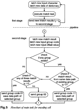
latch new input character latch new data of dictionam
,
" Iexecute match task
to second stage
Dioeiine ..._...~..
latch new input group code latch new inDut offset value
\ J
r
yes
check match result from same data path
of existing group is 'l'? check if WS"1tS i s ' l 7 ves -U' Fig.5 Flo,vchmt of mani taskfor ncoding Lell
The selected group in cell k will he transmitted to cell k ~
1, and it of cell k ~ 1) becomes a candidate to compete
with the eight comparison results of cell k ~ 1 after four
clock cycles. If the group leader of lk-l fxst appears in cell k - 1, the (length, offset) data of lk-l will be transmitted to cell
k ~ 2. As shown in Fig. 4 the group composed of string
{group} becomes the unique group in cell k - 1 from clock cycles 4 to 8, so the switch position of cell k ~ 1 is allocated
Ni node. Therefore the (length, offset) data of comparison IEE Proc.-Circuifs Devices Sysl., Vol. 146, No. 5. October 1999
results between the first five input characters {group} and the encoded string {D3D4DsD6D7} in cell k will be trans- ferred transparently from cell k to cell k - I, cell k ~ 2, ._.
and the final stage (cell 0) according to the amval time of group leader in the future consecutive cells.
As described in Fig. 4, the main task of the encoding cell is to control the switch position. If the amval time of any group leader is earlier than the others, the switch position of that encoding cell will be switched to the node that can construct a data path for the optimal group leader to pass, such as node N4 of cell k during clock 0 or node
N,
of cellk - 1 during clock 4 in Fig. 4. The flowchart of the encod- ing cell's main task can be shown as Fig. 5, where codes 01 and 11 indicate that the character is a group leader and a group member, respectively. Code 00 indicates that the character does not belong to any group. Switch S of the encoding cell shown in Fig. 3 can be treated as a finite state machine which can save the data path of the existing group and control the switch position. If one data path is selected in this encoding cycle, it has the highest priority to be selected during the next encoding cycle, e.g. the fxst group string {group} in cell k from cycles 0 to 4 and in cell
k - 1 from cycles 4 to 8, respectively. On the contrary, the finite state machine will select the optimal data path again when the original data path gets an unmatched result dur- ing the next encoding cycle. For example, during clock cycle 9, in cell k - 1 the switch position is switched to N7
position.
Table 1: Transition table of finite state machine for each state register
Current state Current input N L l l I Next state a( ti+ Tdr) mtl+rdJ
N(tl+rd,+rdx)
cttl+r+rd,,)
1 0 X O 1 1 X 1 0 0 X O 0 1 1 1 0 1 0 0 Z clock periodtr: oositive edae time for the current clock clcve Niill: inversLvalue of L, Ill, MSB of L,
Jd; delay time of D type register for latching new data '
Ti; delay time of combinational logic circuit for NL I11 Td,j delay time of one AND gate
F(tl+JdJ: lo (tl+Td,)for qon, ll (tl+Jd,) for qln, ..., I,(t,+T,Jfor qkn
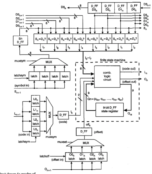
The block diagram of the modified encoding cell is illus- trated in Fig. 6, where the diagram of the fmite state machine is marked by the dash line, and its transition table is shown in Table 1. In Fig. 6, nine state registers are used to generate a new group code L, and its appending offset
values 0,. The individual value of lo-17 is equal to 1 when the respective comparison result is matched, othenvise it is 0 for unmatched status. These fdtered group codes and their appending oflet values amve at the MONITOR to generate the optimal code pair (length, offset). From now on the main task of the encoding cell can be adjusted to encode the group codes based on the current match results, the current state, and the current incoming group code as follows: MSB Ln[l] = (lo Q O ~ )
+
(11 41%)+
( h
.
~ 2 % )+
. . .+
( l , ' %)+
(lk ' %k) (1) LSB L,[0] = lo+
ZI
+
12+
. . .+
Z7+
l k (2) 271latchsyrn
A
Fig. 6 Circuit diagramfor Wcoalig cell
muyset
latchoff
where symbol
'+'
and symbol '.' represent logical AND and OR operators, respectively. We use a simple finite state machine circuit to generate the optimal group code accord- ing to la ~ j7, and lk so that neither counter nor magnitudecomparator are needed. This system has been implemented by using a 0 . 6 ~ standard cell library, e.g. provided by Compass Company, USA.
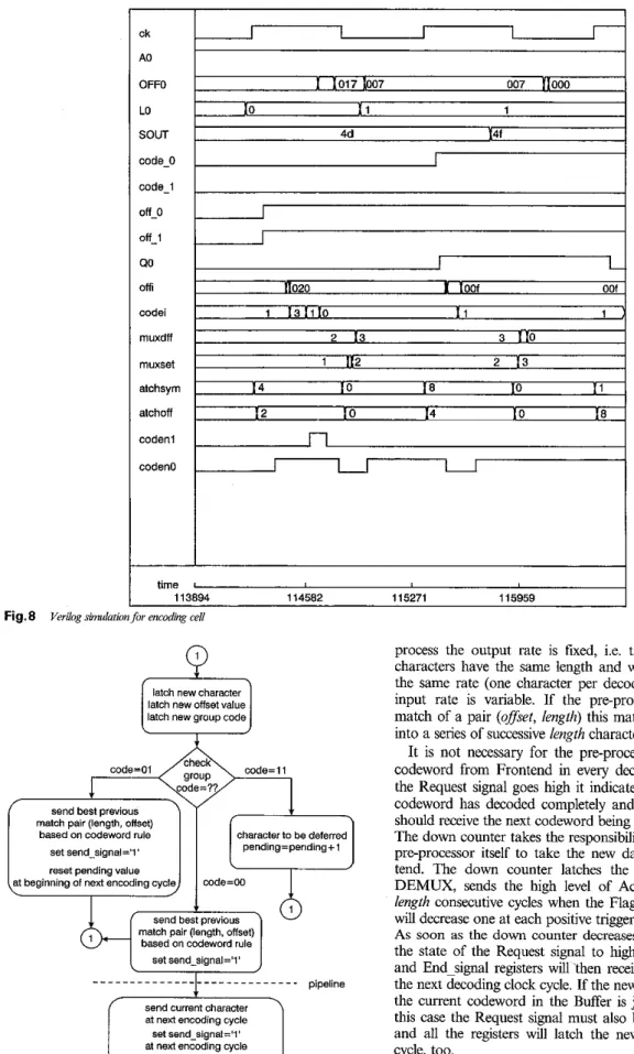
The timing sequence of the encoding cell given in Fig. 6
is shown in Fig. 7. At O n e Tn for encoding cell n, all of the D-type flip-flops latch the individual new values, then com- pare the input character S,, with the eight encoded charaG ters D3,-DOn of cell n and D3,+,
-
DO,,, from the dictionary registers of cell n+
I. The current comparison results &-I7 and lk are transmitted to the f i t e state machine to obtain a new code L, and the new next state Qni. At time Tn+
T, cell n latches the new state of group leadersQn,
where Q, is composed of qnn, qln, ..., q7", qh. Finally, encoding cell n utilises the new state values to obtain the new offset output value 0,. Thus the encoding cell is separated into two pipeline stages to execute the encoding process for one input character. As simulated by the Synopsys synthesis tool, the critical path of cell n isidentifed from the Sa, D3,-DOa, and D3,+,-DO,+, to the output of the new code L,. The critical path delay is about 7ns, calculated from positive edge ck to
M
as shown in212
Fig. 8 by Verilog simulation. Hence the clock period T
should be larger than 7ns to get the correct e n d i n g results for the encoding cell.
3.1 Monitor module
As depicted in Fig. 9, the monitor module receives the character, offset and group codes from cell 0 and decodes the longest length based on g o u p code, where the longest length is equivalent to p e d h g values in Fig. 9. The main function of the monitor, as shown in Fig. 9, is to indicate whether one codeword is found or not by the send signal.
Suppose a pointer uses the space of p uncoded charac- ters, the encoding rule is based on the length value of the codeword. If the length value is greater than that of p , the monitor will send the codeword. Otherwise, the monitor sends the uncoded character.
3.2 Packet module
The packet module receives codewords from the monitor, concatenates these codewords together and segments them into 16-bit words for output. In [12], encoding and decod- ing buffers have been employed for the HUmnan coding algorithm. Since the Huffman code has variable-length codewords it needs a complicated programmable logic array @)AL' to record the lengths of the individual code
I To+2T ITo+3T
,
To+4T T0+5TI TO I
I I I
I
IJo(
I I I
musym se& 0 select I select2 select 3 select0 select 1
D3,-DO,, S,. lk. 0.
N
N
36(
36(
IO"l7 I)# I I I
I I I I
new state of
I
valid valid valid valid validgroup leader Q" Qn Qn Qn Q"
I
I
I I I I Imuxset I select 0
X
selict 1X
s e i ~ c t 2X
sele'ct3X
seidctoI I I I latchoff I I
I
Fig.1 T b n i ~ s e y u e n e e f o r d ~ e Uwords for executing the packing task. The LZSS codeword has two codeword formats, i.e. uncompressed and com- pressed forms. Thus, it is not necessary for the LZSS
code-
word to utilise the PLA table. In our design a simple combinational logic circnit instead of the PLA table is used to control the barrel shifter.
The circuit diagram of the packet module is shown in Fig. 10. The 16-bit register W2 is the output latch. If the sum of Residue and Length is greater than 15, the Full out- put of the accumulator will be set to High and the packet module will put the contents of the W2 register at the posi- tive trigger of Out-clock signal. Since the maximum bit- number of the concatenation of Flag and codeword is greater than 16, the sum of Length and Residue may be equal to 32, sum of 17 and 15. In this case there are two 16-hit packets being ready for output, the system will send W2 contents frst and then W3 contents at the positive trig- ger of Out-clock and that of Out-again, resptively. Here Out-again is generated hy Next-any signal of the accu- mulator.
The parallel concatenation of codewords is done by MUXl and Barrel_Shifter, which provide 16-bit windows on their 33 input hits. MUXl is controlled by the Flag sig- nal and shifts the codeword from WO into W1 so that the rightmost bit of W1 is the last hit of the codeword. Conse- quently the data stored in W1 is ready to concatenate with the next codeword. The Barrel-Shifter is controlled by the residue value which represents the number of the residual bits in W1. The residnal bits in W1 are determined hy MUXI.
3.3 Sender module
When the Over signal of the packet module falls from high to low the system is to f k h the encoding process. When
IEE Proc.-Cilcuils Devices Sysl.. Vol. 146, No. 5, Oelober I999
the value of the residue register is not equal to zero all the final residual bits in W2 or Barrel-Shifter must be sent to the sender module for output. If the packet module has just sent an output in the previous ckl cycle, the 16-bit output of Barrel-Shifter is sent to sender. Otherwise, packet sends the 16-bit output of register W2.
4
A block diagram of the decoding processor is shown in Fig. 11. The functions of the major modules are described as follows. The input to the Frontend is a bit stream with- out explicit word boundaries. The Frontend has to decode
a codeword, determine its length and Flag, and shift the input data stream hy the number of bits corresponding to the decoded code length before decoding the next code- word. The pre-processor separates the codeword into the corresponding offset and character parts, and generates Active=l for the successive length cycles. As the system receives a Ready signal the counter generates three enable signals to start the decoding process. As enable-0 rises to high, the 16-bit register W1 stores the fmt 16-bit register. During enable-1 cycle, W1 stores the second 16-bit input stream and the fust 16-bit input stream must be shifted into WO. The flag and length of the frst codeword are deter- mined at the same cycle. When the enable-2 signal goes high the Frontend produces the fmt codeword and its flag, and the system begins to enter the normal decoding process in the consecutive cycle.
The circuit diagram of the preprocessor for decoding is shown in Fig. 12. The pre-processor has to separate the codeword into character and offset, generate the Active sig- nal to the rightmost cell, and send a Request signal to Frontend to process the next best match. In ow decoding
VLsl design of decoding scheme
ck A0 OFF0 LO SOUT code-0 code-1 off-0 off-I QO Offi codei muxdn muxset alchsym atchofl codenl coden0
match pair (lengm, onset) based on Codeword rule
Set Send_SiQnal='l' reset pending value
I
Ir-
1
10171007 007 !(OOO l o 1 1 1 4d 14fI
character to be deferred pending=pending+lI---"
I
a1 beginning Of next enmding cycle
time 8
113894 114582 115271 1 15959
w d e = w
1
send best previous
match pair (length, onset) based an codeword rule
pipeline
at next encoding cycle
Set send_signal='l' at next encoding Cycle
reset pending value Fig. 9 %wc!mt ofmvniror morhrle
214
process the output rate is fixed, i.e. the output decoded characters have the same length and will be generated to the same rate (one character per decoding cycle), but the input rate is variable. If the pre-processor receives the match of a pair (offset, length) this match will he decoded into a series of successive length characters.
It is not necessary for the pre-processor to receive the codeword from Frontend in every decoding cycle. When the Request signal goes high it indicates that the previous codeword has decoded completely and the huffer register should receive the next codeword being ready for decoding. The down counter takes the responsibility of informing the preprocessor itself to take the new data from the Fron- tend. The down counter latches the length value from DEMUX, sends the high level of Active signal for the length consecutive cycles when the Flag is equal to 1, and will decrease one at each positive trigger of ck timing clock.
As soon as the down counter decreases to two it changes the state of the Request signal to high. The Buffer, Flag and Endsignal registers will 'then receive the new data in the next decoding clock cycle. If the new Flag is equal to 0,
the current codeword in the Buffer is just a character. In this case the Request signal must also be changed to high
and all the registers will latch the new data in the next cycle, too.
Dataflow in the systolic array of the series decoding cell has been described in previous literature [Ill. The main task of the decoding cell n is to compare the input oflet
value with the stored oflet values in cell n, where the stored ofset values are 2n and 2n
+
1 when the cell number is n. If the input oflet value is equivalent to one of the stored offset values 2n or 2n+
1, the output decoded char- acter willbe
copied from S, register or Sa+, register, repeo tively, where Sn+l register comes from the preceding stage (cell n t I). Othenvise, the input character is retransmitted to the next stage (cell n - 1). The original characters will be recovered without distortion by the systolic array of the series decoding cell. The decoding cell [ll] is shown in Fig. 12.5 analysis
The new encoding architecture is implemented by the 0 . 6 ~ standard ceU library supported by the Compass Company in the USA. We utilise the synthesis tool from Synopsys to synthesise the Verilog RTL code to gate-level schematic. The hardware cost including the estimated equivalent wire load for each module and encoding cell were listed in Table 2. In this encoding system the buffer size of the encoding window is 512, and the total gate
Hardware synthesis and simulation and power
active over-signal
c k l c k l
select one to output under specified condnion
out={WO[16:8], W1[6:0]} > >codesize+residue-16 send send3 send
-
out-again= f out-again+
out_clock+
enable-2-trontendeady-
... ... ?si- character ""'...
processor...
-
...
~ 1 275VLcell Receiver Monitor Packet Sender Module name
Gatecount (including 1345 21771 88472 364.5 346 1376.7 275.12
wire load calculated by
equivalent gate count1
Total 90472.8
Vcell
Cell (64 Cellsl (256 Cellsl
count, not including U 0 pads, is about 90473 gates. The gate count is less than that in other architectures [8] with the same buffer size.
To verify our encoding system we compare the input strings of encodmg processor with the output strings of the decoding processor whose block diagram is shown in Fig. 1 1. If there is no difference between them the modified architecture should be correct. We use some input fdes for verification by Verilog simulator [13]. From these simula- tion results we verity that our encoding and decoding cir- cuits are correct. The hardware simulation results of the whole chip including U 0 and power pads are shown in Fig. 13. The DATA of Fig. 13 is the data output consist- ing of flag and encoded codeword. The SEND signal is the handshaking signal to inform the receiver whether the encoding system transmits output data or not. The low level of the FINISH signal indicates that the encoding sys- tem has fmished the entire encoding task. As shown in Fig. 13, the function of our encoding system can work cor- rectly even when the clock cycle is about 11 ns. The operat- ing frequency is the reciprocal of the clock period so the maximum operating frequency can reach 91 MHz and the compression hit rate is about 728Mbitls. To reduce ground bounce noise for high-speed application we use ten pairs of power pads for the drivers of VO pads, and six pairs of power pads for the core of digital circuit and predrivers of U 0 pads. The total VO pin count is 128.
276
For high speed-application power consumption is an important issue. The gate count of the registers contributes the major part of the hardware for most LZ-type compres- sors. In the Zit+Wolfsystem each register must access and latch new data in every clock cycle, and thus the dynamic power consumption is very large. As described in [14], we estimate the percentage activity of the circuit
Pa
and the total capacitance C, driven by gate outputs in circuit. Thus, the estimated power consumption of the complex circuit for CMOS design can be estimated as follows:where
f,
is the clock frequency. From eqn. 3, minimising the percentage of the switching capacitance Pa can save power dissipation. In our design only one quarter of regis- ters execute the data access operation for input characters, codes, and offsets as shown in Fig. 7 during one clock cycle. Therefore minimising the number of memory accesses will reduce the power dissipation for the sake ofreducing P,. The number of memory accesses for our encoding cell is about 7/19 of the Zitc-Wolf architecture [I I], so that the dynamic power dissipation can he lowered with the same throughput rate. Since our implementation is based on CMOS design, there is no DC path during the operating cycle. For the CAM implementation [7l the DC path exists in the circuit of the CAM cell such that the power dissipation of CAM architecture is larger than the CMOS design under the same throughput rate, clock fre-
Pd =
Pa
xc,
x V i D x fc (3)-
ck cr SING SIN s o n ACT1 A0 OFF0 LO CODEIN topck OFFlN SEND DATA FINISH-
I
L
00 00 01 165 65 y20 20 163 143 163 120I
OM I008 rood rOM 10071 1 y o
11
1
I
I
I
1
000 000 ~ 10542 0542 lad4a la948 time,
4 91270 91&0 92410 92980 Fig. 13quency, and the same buffer size conditions. For high- speed applications the power dissipation of our architecture implemented by CMOS process is lower than those of the other implementations for the same compression ratio.
6 Conclusion
A parallel structure for a high-speed LZSS coder has been introduced. This parallel LZSS coder encodes each charao ter in one clock cycle, and its operating frequency can reach 91MHz. This system has several advantages. First, the compression time is linearly proportional to the input length. Only a single clock cycle is required for processing one character, and the clock cycle is bounded by the critical delay of the encoder and independent of window size. S e 0
ondly, the architecture is simple and modularly expandable. In our design only 256 encoding cells are integrated in one chip at most because of the problems of power, clock dis- tribution, and hardware complexity. We can cascade sev- eral chips to increase the dictionary buffer size and achieve
the ideal desired compression ratio.
Although the hardware complexity of our modified architecture is higher than those of other architectures in [4, 61, the speed is much higher. Suppose the trigger cycle C,.ig represents the numbcr of time unit (clock cycle) between two initiations of a pipeline. A trigger cycle Clrig of k means
that two initiations are separated by k clock cycles. Assume
the clock period is T,. The average compression speed bit %/e eh@ ~imulatwn by VedoC sirnuloror
IEE Proc.-Circuifs Devices Sysr., Vol. 146, No. 5. Ocrober 1999
rate of our architecture is (1
*
8)/(Ctri,*
T J , where C,, isequal to one, and T, = Tdl,,el + TdIood-Gecp Assume M and N represent the maximum length of the matching string and buffer size, respectively. The muximm compression speed bit rate in [4] is ( M
*
X)/(T,*
Cl,ig), where Clrig is equal to (Ni2) + M. If we want to achieve the ideal com- pression ratio, the encoding buffer in [U] is 512 at least. Our C,". is much lower than that of [4, 61, so our speed is apparently higher for the same process technology. Thns, the new compression system is more suitable for real-time application to increase the bandwidth of a communication system and can also be used to effectively increase the amount of mass storage available to computer systems. By utilising VLSI technology to implement the system chip, the data compression hardware can be integrated into real- time systems so that data can be compressed and decom- pressed on-the-fly.7 Acknowledgment
This work was supported by the National Science Council of Republic of China under grant NSCX2-0404-E009-338.
8 References
1
2
ZN, J., and LEMPEL, A.: 'A miversal algorithm for sequential data compression', IEEE Tram, lnf Theory, 1977, IT-23, pp. 337-343 ZlV, J., and LEMPEL, A.: 'Compression of individual sequence Via
variable-rate coding', IEEE Trons. Inf Theory, 1978, ll-24, pp. 5 3 k 536
3 BELL, T.C.: 'Better OPML text compression', IEEE Trans. Corn- mun, 1986, COM-34, pp. 11761182
4 JUNG, B., and BURLESON, W.: 'A VLSI systolic array architecture for Lempel-Ziv-based data compression'. Proceedings of IEEE inter- national symposium an Cicuit and systems, June 1994, Vol. 3, pp. 6 s
68
STORER. J.A.: 'Data cammession: methods and theorv' (Cornouter
9 STORER, J.A.: 'Image and text compression' (Kluwer Academic Publishers, Norwell, Massachusetts, 1992)
10 K ~ G ,
s , y
'vu1 array processors~ (fientice.~dl, Englewood ClitTs, NJ, 1988)11 ZITO-WOLF, R.J.: 'A systolic architecture for sliding-whdow data compression'. Proceedings of IEEE Workshop on VLSI sig,ialprocess-
5
7 LEE, C.Y., Gd YANG, R.Y.: 'High-throughbht- data winpassor
design using content addressable ~ E E proe cjrails ~ ~ ~ i , . ~
S p t . . 1995, 142, (I), pp. 69-73
CHEN, C.T., and CHEN, L.G.: 'A novel architecture far LernpeI- Ziv-based data compression'. Proceedings of ICCE international con- ference on Consumer ekoronicr, 1996, pp. 21t&211
13 Cadence Design System Inc., Venlog-XL manual, version 1.7, Sept. 1993
14 WESTE, N.H.E., and ESHRAGHIAN, K.: 'Principles of CMOS VLSI design: a perspective system' (Addison-Wesley Publishing Com- pany, 1993, 2nd ed".), pp.236-238
8