System Modeling and Analysis of Single-Phase Current Regulation Module
(1)Ray-Lee Lin
(1)National Cheng Kung University No. 1, Ta-Hseuh Road
Tainan City, Taiwan [email protected]
(1, 2)Wei-Jhih Wun
(2)Richtek Technology Corporation 5F, No. 20, Tai Yuen Street, Chupei City
Hsinchu County, Taiwan [email protected]
Abstract -- This paper presents the system modeling and analysis of the single-phase current regulation module (CRM) in continuous-conduction-mode (CCM) at steady state for use in the electrical discharge machines (EDMs). Based on the equivalent model of the three-terminal PWM switching cell, the small-signal equivalent circuit models of the single-phase CRM are obtained to derive the corresponding open-loop transfer functions, including control-to-output, line-to-output, output admittance, and input impedance. The derived theoretical transfer functions are verified with the measured results of a prototype circuit.
Index Terms – modeling, current regulation model, CRM, transfer function, electrical discharge, EDM
I. INTRODUCTION
Unlike the conventional contact-type grinding and milling machines, electrical discharge machines (EDMs) of non-contact type are suitable for the accurate concave-shape machining on hard materials with conductivity [1].
Fig. 1 shows the conceptual EDM machining process [2], where the EDM functions as a current source to provide a stable discharging arc between an electrode and a workpiece in dielectric fluid. Before the discharging state, the voltage is applied on the gap by the current source and the impedance of the gap keeps at the high-impedance state.
While the electrode is moved down and starts to discharge on the workpiece, the impedance between the electrode and the workpiece behaves simply equivalent to gap-resistor R in parallel with a parasitic capacitor C [3-5]. The value of this parasitic capacitor C is determined by the geometrical distance and areas of the electrode and the workpiece. Once the electrode is moved up, the impedance of the gap returns to the high-impedance state. The pulse-type discharge current, as shown in Figure 1, is demanded for the applications of the EDMs [6-9].
Similar to voltage regulation modules (VRMs) [10-13], the CRMs provide the pulse-type output current to generate the discharging arc to the workpiece through the gap, as the function of the EDMs [14,18]. Among these prior works, two interleaved four-phase buck-based current sources utilizing different energy-recovery schemes, proposed in [2, 17, 18], for EDMs are used to provide pulse-type current waveform with high slew-rate and flat plateau at steady state.
However, the works of system modeling analysis have been
not yet detailed yet for these two newly proposed CRMs working at steady state.
Fig. 1. Conceptual EDM machining process [2].
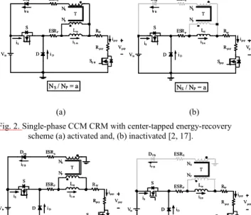
Since the interleaved four-phase buck-based current sources utilize different energy-recovery schemes at steady state can be further simplified as an equivalent single-phase CCM CRM [2, 17, 18], the theoretical transfer functions of the CCM CRMs will be presented in this paper. Due to the high conductivity of the ionized discharge path, the gap equivalent circuit, as shown in Figure 1, can be further simplified as the gap-resistor R by neglecting the gap-capacitor C. Under this assumption, the single-phase CCM CRMs with the center-tapped energy-recovery scheme [2, 17] or the isolated energy-recovery scheme [2, 18] can be simplified in terms of the input DC-voltage source, Vin, the coupled inductor T, the wire resistor RW, and gap-resistor Rgap in series with the switch Sgap, as shown in Fig. 2(a) and 3(a), respectively.
While the main switch S1 and the switch Sgap are turned on, the input DC-voltage source Vin begins to charge the magnetizing inductor Lm of T and provide the gap current igap. Meanwhile, the current path to the input DC-voltage source Vin, in the energy-recovery schemes are blocked by the free-wheeling diode DFB, as shown in Fig. 2(b) and 3(b), respectively.
When the switch, Sgap is turned off to emulate the condition that the electrode moves away from the workpiece, the discharge current in the gap becomes zero. Therefore, the residual energy stored in the magnetizing inductor Lm of T is then transferred from the primary side to the secondary side of T through the free-wheeling diode DFB to the input DC-voltage source Vin.
Lm
T S
D NP
Vin
Rgap
igap
ESRP
NS/ NP= a
NS
ESRS
DFB
iF B
iD
iS iL m
Sg ap
Vgap
RW
Vg ap
Lm
T S
D NP
Vin
Rgap
igap
ESRP
NS/ NP= a
NS
ESRS
DFB
iF B
iD
iS iLm
Sgap
RW Lm
T S
D NP
Vin
Rgap
igap
ESRP
NS/ NP= a
NS
ESRS
DFB
iF B
iD
iS iL m
Sg ap
Vgap
RW
Vg ap
Lm
T S
D NP
Vin
Rgap
igap
ESRP
NS/ NP= a
NS
ESRS
DFB
iF B
iD
iS iLm
Sgap
RW
(a) (b) Fig. 2. Single-phase CCM CRM with center-tapped energy-recovery
scheme (a) activated and, (b) inactivated [2, 17].
Lm
T S
D NP
Vin
Rgap
igap
ESRP
NS/ NP= a
NS
ESRS
DFB
iF B
iD
iS iL m
Sg ap
Vgap
RW
Vgap
Lm
T S
D NP
Vin
Rgap
igap
ESRP
NS/ NP= a
NS
ESRS
DFB
iF B
iD
iS iLm
Sgap
RW
Lm
T S
D NP
Vin
Rgap
igap
ESRP
NS/ NP= a
NS
ESRS
DFB
iF B
iD
iS iL m
Sg ap
Vgap
RW
Vgap
Lm
T S
D NP
Vin
Rgap
igap
ESRP
NS/ NP= a
NS
ESRS
DFB
iF B
iD
iS iLm
Sgap
RW
(a) (b)
Fig. 3. Single-phase CCM CRM with isolated energy-recovery scheme (a) activated and, (b) inactivated [2, 18].
II. DC AND SMALL-SIGNAL ANALYSIS OF SINGLE-PHASE CCMCURRENT REGULATION MODULE
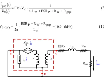
With the three-terminal PWM switch cell, as marked in Fig. 4, the small-signal system block diagram of the open-loop single-phase CCM CRM without energy-recovery scheme is composed of three open-loop small-signal transfer functions: control-to-output Gd, line-to-output GV, and output admittance YP, as shown in Fig. 5.
Fig. 4. PWM switch cell in single-phase CCM CRM without energy-recovery scheme.
Fig. 5. Small-signal system block diagram of open-loop single-phase CCM CRM.
0 Vˆ Vˆ d gap
gap
dˆ in
G =iˆ = = (1)
0 dˆ in Vˆ V gap gap
Vˆ G iˆ
=
= = (2)
0 dˆ gap Vˆ P gap gap
Vˆ
Y = iˆ = = (3)
The relationships in average among the port waveforms of voltages and currents, shown in Equations (4) to (7), can be represented with the circuit configuration of the DC model and the small-signal model for the three-terminal PWM switch cell [19, 20] employed in Fig. 6(a) and 6(b), respectively.
c a D I
I = ⋅ (4)
ap
cp D V
V = ⋅ (5)
dˆ I iˆ D
iˆa = ⋅ c+ c⋅ (6)
dˆ V vˆ D
vˆcp= ⋅ ap+ ap⋅ (7)
(a) (b)
Fig. 6. (a) DC model, and (b) small-signal model for three-terminal PWM switch cell.
By applying the DC and the small-signal model of the three-terminal PWM switch cell, as shown in Fig. 6, the open-loop transfer functions in the small-signal block diagram, as shown in Fig. 5, is derived as follows.
Moreover, the frequencies of the poles and zeros in the open-loop transfer functions can be obtained by utilizing the circuit specifications and parameters listed in Tables I and II, respectively.
Table I CIRCUIT SPECIFICATIONS OF SINGLE-PHASE CCMCRM.
Specifications Values Rated input voltage Vin = 15 V DC
Rated average gap current igap_avg = 1.5 A Switching frequency fS = 150 kHz Equivalent gap resistance Rgap = 3Ω
Table II CIRCUIT PARAMETERS OF SINGLE-PHASE CCMCRM.
Parameters Values Steady-state duty cycle D = 32.5 %
Inductance Lm = 50μH
ESR of inductor ESRP = 25 mΩ Wire resistance RW = 400 mΩ PWM gain
5 . 1 FM= 1
A. DC Analysis
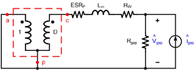
By applying the DC model of the three-terminal PWM switch cell, as shown in Fig. 6(a), the equivalent circuit for the open-loop DC analysis can be constructed, as shown in Fig. 7. This equivalent circuit is composed of a three-terminal PWM DC model, inductor equivalent series resistance (ESR), wire resistor RW, and gap resister Rgap.
The DC transconductance of this equivalent circuit can be determined from Equation (8).
gap W P in
gap
R R ESR D 1 V i
+
⋅ +
= (8)
Fig. 7. Equivalent circuit for derivation of open-loop DC analysis.
B. Open-loop Control-to-Output Transfer Function
By utilizing the three-terminal PWM small-signal model, the small-signal equivalent circuit of open-loop control-to-output can be constructed with perturbation only on duty-cycle, as shown in Fig. 8, in order to derive the open-loop control-to-output transfer function, as shown in Equation (9). Meanwhile, the pole fP-CtO in Equation (9) can be calculated as 10.9 kHz from Equation (10) in terms of the inductance of Lm, the ESR of the inductor, ESRP, wire resistor RW, and gap resistance Rgap according to the circuit specifications and parameters listed in Tables I and II, respectively.
( )
( ) in m P W gap
gap
R R ESR L s V 1 s FM c Vˆ
s iˆ
+ + +
⋅ ⋅
⋅
= (9)
10.9 L =
R + R + ESR 2π
= 1 f
m gap W CtO P
-
P ⋅ (kHz) (10)
Fig. 8. Equivalent circuit for derivation of open-loop control-to-output transfer function.
C. Open-loop Line-to-Output Transfer Function
By replacing the three-terminal PWM switch cell with the three-terminal PWM DC model illustrated in Fig. 6(a), the small-signal equivalent circuit for the derivation of the open-loop line-to-output can be built, as shown in Fig. 9, with considering the small-signal perturbation applied on the DC-input voltage source only.
In order to analyze the audio-susceptibility of the open-loop system, open-loop line-to-output transfer function can be obtained, as shown in Equation (11), by applying the equivalent circuit illustrated in Figure 9. The pole fP-LtO as a function of the inductance of Lm, inductor ESR, wire resistor RW, and gap resistance Rgap in Equation (12) can be computed with the circuit specifications and parameters listed in Tables I and II, respectively.
( )
( ) m P W gap
in gap
R R ESR L s D 1 s Vˆ
s iˆ
+ + +
⋅ ⋅
= (11)
9 . L 10
R R ESR 2 f 1
m gap W LtO P
P + + =
π⋅
− = (kHz) (12)
Fig. 9. Equivalent circuit for derivation of open-loop line-to-output transfer function.
D. Open-loop Output-Admittance Transfer Function With the perturbation only applied to the output load current, the open-loop output-admittance transfer function can be derived according to the equivalent circuit illustrated in Fig. 10. The open-loop output-admittance transfer function includes one zero, fZ-OA, and one pole, fP-OA, as shown in Equation (13). According to the circuit specifications and parameters listed in Tables I and II, respectively, the zero fZ-OA in Equation (13) as a function of the inductance of Lm, the ESR of the inductor, ESRP, wire resistor RW, and gap resistance Rgap can be calculated as 10.9kHz using Equation (14). Unlike the fZ-OA, the pole fP-OA
in Equation (15) is only determined by the inductance of Lm
and the ESR of the inductor, ESRP, wire resistor RW, but not gap resistance Rgap.
( )
( ) ( m P W) gap
gap W P m gap
gap
R R ESR L s
R R ESR L s s Vˆ
s iˆ
+ +
⋅
+ + +
= ⋅ (13)
9 . L 10
R R ESR 2 f 1
m gap W OA P
Z + + =
π⋅
− = (kHz) (14)
35 . L 1
R ESR 2 f 1
m W OA P
P + =
π⋅
− = (kHz) (15)
Fig. 10. Equivalent circuit for derivation of open-loop output-admittance transfer function.
E. Open-loop Input-Impedance Transfer Function
With only the small-signal perturbation on the DC-input voltage source, the small-signal equivalent circuit for the derivation of the open-loop input impedance can be constructed, as shown in Fig. 11.
According to the equivalent circuit illustrated in Fig. 11, open-loop input-impedance transfer function can be obtained, as shown in Equation (16). With the circuit specifications and parameters listed in Tables I and II, respectively, the zero fZ-II in Equation (16) can be calculated as 10.9 kHz from Equation (17) in terms of the inductor, inductor ESR, wire resistor RW, and gap resister Rgap.
( )( ) m P2 W gap
in in
D
R R ESR L s s iˆ
s
Vˆ ⋅ + + +
= (16)
9 . L 10
R R ESR 2 f 1
m gap W II P
Z + + =
π⋅
− = (kHz) (17)
Fig. 11. Equivalent circuit for derivation of open-loop input-impedance transfer function.
III. EXPERIMENTAL RESULTS
By using the Gain/Phase Analyzer, PSM1735, the measured Bode diagrams can be obtained from the prototype circuit of the single-phase CCM CRM, which is built according to the circuit specifications and parameters listed in Tables I and II, respectively. The Bode diagrams plotted from the derived open-loop transfer functions of the single-phase CCM CRM are compared with those measured Bode diagrams, as shown in Figs. 12, 13, 14, and 15.
The measured and the calculated Bode plots of the open-loop control-to-output transfer function are shown in Figure 12, which illustrate that the experimental results are promisingly in consistent with the calculated model till 150 kHz. The pole fP-CtO in the open-loop control-to-output magnitude Bode plot is approximately at 10.9 kHz. Besides, the DC gain of the open-loop control-to-output magnitude
Bode plot at 100 Hz is approximately equal to10 dB.
Fig. 13 illustrates the comparison between the experimental Bode plots of the open-loop line-to-output transfer function and the corresponding calculated results.
Before the switching frequency 150 kHz, the measured magnitude Bode plots and the corresponding calculated model are in close agreement. Unlike the experimental magnitude Bode plot, the measured phase Bode plot is not in close agreement after 30 kHz. Additionally, the pole fP-LtO in the open-loop line-to-output magnitude Bode diagram is approximately at 10.9 kHz.
The measured Bode plots of the open-loop output-admittance transfer function and the corresponding calculated results are compared, as shown in Fig. 14, in which the experimental and calculated models are favorably similar with each other. The zero fZ-OA in the magnitude Bode diagram of the open-loop output-admittance is approximately at 10.9 kHz. In addition, the pole fP-OA
approximately locates at 1.35 kHz.
With the setup of the small-signal perturbation used in the previous measurement of the open-loop line-to-output transfer function, the experimental Bode plots of the open-loop input-impedance transfer function, as shown in Figure 15, are obtained and compared with the corresponding calculated results. Before the half of the switching frequency 75 kHz, the comparison shows that the experimental and the calculated models are consistent promisingly with each other. The zero fZ-II of the open-loop input-impedance magnitude Bode plot approximately locates at 10.9 kHz.
IV. CONCLUSIONS
This paper has presented the system modeling and analysis of the single-phase CCM CRM in steady state for use in the EDMs. For the given circuit specifications and parameters, the experimental results agree closely with the calculated results of the corresponding derived transfer functions. The derived open-loop transfer functions reveal that the inductor, Lm, and the ESR of the inductor, ESRP, dominate the frequencies of the poles and zeros in the open-loop transfer functions of the single-phase CCM CRM.
Therefore, the frequencies of the poles and zeros can be calculated from the open-loop transfer functions of the single-phase CCM CRM by using the given circuit specifications and parameters.
ACKNOWLEDGEMENTS
This work was supported by the National Science Council (NSC), Taiwan, under Award NSC 97-2221-E-006 -275-MY2, and also made use of Shared Facilities supported by the Program of Top 100 Universities Advancement, Ministry of Education, Taiwan. Besides, the authors would like to appreciate Mr. W. Hsu, CEO, Yihawjet Enterprises Company Ltd., Tainan City, Taiwan, for his invaluable technical discussions on electrical discharge machines.
Fig. 12. Measured Bode diagrams of open-loop control-to-output transfer function.
Fig. 13. Measured Bode diagrams of open-loop line-to-output transfer function.
Gain ( dB )
Fig. 14. Measured Bode diagrams of open-loop output-admittance transfer function.
Gain ( dB )
Fig. 15. Measured Bode diagrams of open-loop input-impedance transfer function.
REFERENCES
[1] Complete EDM Handbook, available: http://www.reliableedm.com.
[2] C. C. Hsu, Buck-based current source with energy-recovery scheme for electrical discharge machine, M.S. Thesis, National Cheng Kung University, Taiwan, Nov. 2006
[3] Hoang Vinh Sinh, Banh Tien Long, and Nguyen Cong Hien, “A study of method to control EDM process,” available:
http://www.ritsumei.ac.jp/acd/cg/se/rt/mems/report/HUT-RITS-2004/
Proc/HoangVinhSinh.pdf
[4] A. Behrens, M. P. Witzak, and F. L. Bruhns, “Control and prediction of course of spark erosion process on spark erosion machine,” German Patent DE19 512 291, 1995.
[5] A. Behrens, J. Ginzel, and F. L. Bruhns, “Arc detection in electro-discharge machining,” ISEM XIII Conf. Proc., pp. 283–294, 2001.
[6] N. Saito, K. Kobayashi and T. Oizumi, ‘‘Method and apparatus for electrical discharge machining,” U.S. Patent 3 999 028, 1976.
[7] T. Furukawa, ‘‘EDM pulse generator with a variable output inductor for producing pulse with gradually rising edges,” U.S. Patent 4 441 005, 1984.
[8] Y. Ozaki, K. Tsurumoto, T. Yatomi and M. Yamamoto, ‘‘Electrical discharge machine with control of the machining pulse’s current value in accordance with the delay time,” U.S. Patent 4 695 696, 1987.
[9] B. Sen, N. Kiyawat, P. K. Singh, S. Mitra, J. H. Ye, and P. Purkait,
“Developments in electric power supply configurations for electrical-discharge-machining (EDM),” The Fifth International Conference on Power Electronics and Drive Systems, vol. 1, pp.
659-664, Nov. 2003.
[10] M. T. Zhang, M. M. Jovanovic, and F. C. Lee, “Design considerations for low-voltage on-board DC/DC modules for next generations of data processing circuits,” IEEE Trans. on Power Electronics, vol. 11, no. 2, pp. 328-337, March 1996.
[11] X. Zhou, P. L. Wong, P. Xu, F. C. Lee, and A. Q. Huang,
“Investigation of candidate VRM topologies for future microprocessors,” IEEE Trans. on Power Electronics, vol. 15, no. 6, pp. 1172-1182, Nov. 2000.
[12] F. Zhang, J. M. Zhang, D. M. Xu, and Z. Qian, “A novel high performance voltage regulator module,” in Proc. IEEE APEC, vol. 1, pp. 258-261, March 2001.
[13] M. Ye, P. Xu, B. Yang, and F. C. Lee, “Investigation of topology candidates for 48V VRM,” in Proc. IEEE APEC, vol. 2, pp.
699-705, March 2002.
[14] R. Casanueva, L. A. Chiquito, F. J. Azcondo, and S. Bracho,
“Current source LCC resonant converter for an EDM power supply,” in Proc. IEEE IECON, vol. 2, pp. 1027-1032, Dec. 2001.
[15] R. Casanueva, F. J. Azcondo, C. Branas and S. Bracho, “Analysis, design and experimental results of a high-frequency power supply for spark erosion,” IEEE Trans. on Power Electronics, vol. 20, no. 2, pp. 361-369, March 2005.
[16] R. Casanueva, Azcondo, F. J. Azcondo, and C. Branas, “A new bipolar power supply for spark erosion based on a series-parallel resonant inverter,” IEEE Trans. on Power Electronics, pp.
1904-1909, 24-28 Feb. 2008.
[17] Ray-Lee Lin, Cheng-Ching Hsu, and Shih-Kuen Changchien,
“Interleaved Four-Phase Buck-Based Current Source with Center-Tapped Energy-Recovery Scheme for Electrical Discharge Machining,” in Proceedings of IEEE APEC2008, Austin, Texas, USA, Feb. 2008, pp. 1536-1542.
[18] Ray-Lee Lin, Cheng-Ching Hsu, and Shih-Kuen Changchien,
“Interleaved Four-Phase Buck-Based Current Source with Isolated Energy-Recovery Scheme for Electrical Discharge Machining,”
IEEE Trans. on Power Electronics, vol. 24, no. 7, July 2009, pp.
1788-1797.
[19] V. Vorperian, “Simplified analysis of PWM converters using model of PWM switch part I: continuous conduction mode,” IEEE Trans.
on Power Electronics, vol. 26, No. 3, pp. 490-496, May 1990.
[20] E. Vandijk, J. H. N. Spruijt, D. M. Osullivan, and J. B. Klaassens,
“PWM-switch modeling of DC-DC converters,” IEEE Trans. on Power Electronics, vol. 10, no. 6, pp. 659-665, Nov. 1995.
![Fig. 1 shows the conceptual EDM machining process [2], where the EDM functions as a current source to provide a stable discharging arc between an electrode and a workpiece in dielectric fluid](https://thumb-ap.123doks.com/thumbv2/9libinfo/9127782.411928/1.918.483.839.348.550/conceptual-machining-process-functions-discharging-electrode-workpiece-dielectric.webp)