Research Express@NCKU - Articles Digest
Research Express@NCKU Volume 19 Issue 2 - July 1, 2011 [ http://research.ncku.edu.tw/re/articles/e/20110701/1.html ]
Mechanism Investigation of p-i-n ZnO-Based
Light-Emitting Diodes
Ching-Ting Lee
Institute of Microelectronics, National Cheng Kung University [email protected]
1.
I
ntroductionZnO-based semiconductors have been investigated as promising materials for advanced electronic and optoelectronic devices due to wide direct bandgap. However, it is difficult to obtain p-type ZnO and intrinsic ZnO (i-ZnO), because ZnO-based semiconductors are naturally an n-type semiconductor due to the compensation effect of shallow donors induced by oxygen vacancies or zinc interstitials. In this research, two novel methods were developed to obtain p-type ZnO and i-ZnO films. Using AlN codoped ZnO, the cosputting method was
developed to obtain p-type ZnO films. The novel vapor cooling condensation method was developed to deposit i-ZnO films. In view of the successful deposition of p-type ZnO and i-ZnO films, the first p-i-n ZnO-based light-emitting diodes were simply fabricated in the world. By fabricating the structure of p-i-n ZnO light-emitting diodes, the first step used ZnO and AlN as the sputtering targets to cosputter p-ZnO thin film on sapphire substrate, and then the i-ZnO thin film and the In doped n-ZnO (n-ZnO:In) thin film were deposited by the vapor cooling condensation system 2. Experiment procedures
The radio-frequency (RF) magnetron cosputtering system equipped with a dual RF power supply was used to deposit AlN codoped ZnO films on sapphire substrates. Pure ZnO (99.99%) and pure AlN (99.99%) were used as the target materials and the corresponding RF powers were fixed at 100 and 25 W, respectively. During the deposition process, the N /(N+Ar) flow ratio was kept at 4%. To activate the dopants, the samples were postannealed at 450˚C for 10 min in a N ambient using a rapid thermal annealing (RTA) system to achieve p-type ZnO. The mobility and hole concentration of the p-ZnO are 1.35 cm2/Vs and 1.17×1018 cm-3, respectively. The X-ray diffraction spectrum of p-ZnO presented the only diffraction peak of (0002) plane with the crystallized phase of the wurtzite structure. The associated peak position, full-width at half-maximum (FWHM), and lattice constant are 34.34˚, 0.39˚, and 5.221 Å, respectively.
The vapor cooling condensation system was used to deposit the i-ZnO and n-ZnO:In films. Tungsten boats filled with the ZnO powder and ZnO powder/In tablet were heated. The associated vapor gases were directly driven and
thereafter deposited on the p-type ZnO layer to facilitate the formation of the p-i-n structure using a pumping system. The sublimated vapor materials were condensed on the p-type ZnO layer due to the cooling of liquid nitrogen.
Therefore, the high-quality i-ZnO film with low defects and n-type ZnO:In film were then successfully deposited. The measured carrier concentration of the i-ZnO and n-ZnO:In were 7.6×1015 cm-3 and 1.7×1020 cm-3, respectively. The associated mobility of i-ZnO and n-ZnO:In were 3.2 cm2/Vs and 5.0 cm2/Vs, respectively. The mechanisms of high quality i-ZnO films deposited at low temperature were first proposed in the world [1].
3. Experimental results and discussion
To investigate the ultraviolet (UV) emissions of the i-ZnO layer, temperature-dependent photoluminescence was
Research Express@NCKU - Articles Digest
Fig. 1. Temperature-dependent photoluminescence spectra of i-ZnO film and the inset graph is the temperature dependence of FX peak position.
measured using a He–Cd laser (325 nm) as an exciton source. Figure 1 shows the temperature-dependent PL spectra of the i-ZnO layer measured from 10 K to 300 K. Free exciton (FX) at 10 K which was clearly observed indicated that the i-ZnO layer possessed high optical quality using the vapor cooling condensation technique. For the FX emission shown in the inset of Fig.1, an obvious temperature-dependent redshift from 3.375 eV at 10 K to about 3.325 eV at 300 K was observed. This phenomenon indicate that the transition from bound exciton emissions to FX emission due to the thermal dissociation at a higher temperature.
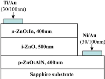
Figure 2 shows the schematic diagram of the fabricated p-ZnO:AlN/i-ZnO/n-ZnO:In LEDs. Figure 3 shows the electroluminescence (EL) spectrum of the p-i-n ZnO-based LEDs operated under different injection currents as a function of photon energy at room temperature. The inset graph is the I–V characteristics of the p-i-n ZnO-based LEDs measured using an HP4156C semiconductor parameter analyzer. The forward turn-on voltage and reverse breakdown voltage are about 2 and −6 V, respectively. The UV emission band centered at about 3.2 eV is attributed to the i-ZnO film without involving any deep level emissions.
4. Conclusions
In this research, cosputter method and vapor cooling condensation method were developed to deposit high-quality p-ZnO film, and i-p-ZnO film and n-p-ZnO:In film on the sapphire substrates. The p-i-n p-ZnO-based light-emitting diodes were fabricated. The EL emission of the p-i-n ZnO-based light-emitting diodes was measured to verify the high performances of the resulting devices. The UV EL peak at 3.2 eV was attributed to the high optical quality with low deep-level defects in the i-ZnO layer deposited by the novel vapor cooling condensation method.
Fig. 2. Schematic diagram of p-ZnO : AlN/i-ZnO/n-ZnO : In LEDs
Fig. 3. Room-temperature EL spectrum of the p-i-n ZnO-based LEDs and the inset graph is the current-voltage characteristic of p-i-n ZnO-based LEDs
Reference
1. H. Y. Lee, S. D. Xia, W. P. Zhang, L. R. Lou, J. T. Yan and C. T. Lee “Mechanisms of high quality i-ZnO thin films deposition at low temperature by vapor cooling condensation technique”, J. Appl. Phys. 108, 073119 (2010).