國立台灣大學電機資訊學院電子工程學研究所 碩士論文
Graduate Institute of Electronics Engineering College of Electrical Engineering & Computer Science
National Taiwan University Master Thesis
超薄金氧半結構電容-電壓與電流-電壓特性之量子力 學模型與驗證
A Comprehensive Quantum-Mechanical Model for C-V and I-V Characteristics in Ultrathin MOS Structure and
Experiment Verification
李建緯 Chien-Wei Lee
指導教授:胡振國博士 Advisor: Jenn-Gwo Hwu, Ph.D.
中華民國 102 年 7 月
July, 2013
Acknowledgement
兩年的研究生生涯終於告一段落了,在碩班期間 受過很多人的幫助與指
導,在此向這些生命中的貴人們表達感謝
首先,感謝指導教授胡振國博士兩年來的指導,在選擇題目上老師給了我 很大的自由度,讓我可以對有興趣的研究題目盡情發揮所長,特別是老師破天 荒的同意了我在碩一升碩二的暑假去東 工業大學做短期研究員,這是唯有對 學生信任而且充分了解學生的指導教授才做得到的,我在此向老師致上十二萬
分的謝意;其次,感謝 CVLAB 的全體成員,因為每一個人 直接或間接的
給予我許多幫助,不論是研究上或是生活上,使實驗室之於我就像是第二個家
一樣溫暖,以下是特別感謝的學長姐:江榮進 許家銘 呂涵薇 柏皓 林
建智 陳姿妤 張博凱 林立 敬凱 楊朝舜 吳侑倫,以及同一屆的:徐
培倫 林星佑 林黃玄,然後是 樂的學弟妹:逄錦昇 廖建舜 廖禹晴,沒 有你們,就沒有這雖然辛苦但卻也無比開心的兩年,願 CVLAB 的溫情能夠一
的傳下去,繼續造福每一個學弟妹;最後是特別感謝的朋友們:陳彥宏 聖為 紀偉廷 張良卉 樓淑 ,雖然研究所期間大家 很忙碌,碰面次數 不多,但你們的存在總是能帶我走出一個個低潮,以及陪我分 生活上的每一 分喜悅,願你們也 能在人生的每一個階段逐夢踏實 得到屬於自己的幸福
要感謝的人 事真的太多了,每一個人 每一件事 是我人生中的寶藏,
如果要把這些 寫進來,那我想一定比這篇論文的正文還要長吧!在寫此謝誌
之時,屬於我自己的人生也即將要起飛了,3 天後是去紐約進行為期近兩個月 的 102 年國際事務青年人才培訓計畫,而 3 個月後則是為期三年的台 電研發
役,那三年 三十年之後呢?充滿未知數的人生,很 我期待 如果把人 生當成一個超巨大的 Monte-Carlo Simulation,那只要盡量讓自己成為一個高能 粒子,那 機的判斷式不論是 Boltzmann Fermi-Dirac 抑或是 Bose-Einstein,
我想 能提高自己跳過 barrier 而進入下一個反應階段的機率吧!
最後,是一個論文寫作者的小小期望,那就是希望這篇論文能對讀者和後 續研究有所幫助,如果把曲高和寡比喻在半導體的載子運動中,那就像是 MOS
的 CLF>CHF一般,本篇論文致力於可讀性的改進,期望能如同載子低頻響應一
般,大家 能有所共鳴
最後的最後,再一次的謝天 陳之藩先生的引用數想必破萬了 ,以及對這 個世界說:我,準備好了!!
李建緯 中華民國 102 年 7 月 3 日
摘要
本研究分為兩大部分 在第一部分中,提出了一個新的統計物理模型,用於 計算二維電子氣之態密度,並提出較精準的表面位能近似方法,用於計算金氧半 結構在 累 強反型區的量子效應 本研究使用指數函數來近似表面位能並解得 表面量子化能階,此外,採用了不準確原理和動量空間中的薛定鍔方程來估算在 二維 三維過渡區的態密度 模擬的結果顯示出我們所提出的近似方法以及態密 度理論可以有效的解決先前研究的兩大問題:因為使用線性函數來近似表面位能 所造成不可忽略的誤差,以及由二維態密度過渡到三維態密度中所產生的態密度 以及電荷濃度分佈的不一致性
在第二部分,我們透過實驗量測出不同氧化層厚度的超薄金氧半結構的電容 -電壓和電流-電壓特性曲線 超薄氧化層結構中的氧化層是由陽極氧化法生長,
而厚度之測定是藉由對比量測所得的電容-電壓曲線與理論的電容-電壓特性曲 線,其氧化層厚度介於 1.8 奈米到 2.8 奈米之間 而在另一方面,自撰程式模擬 的電容-電壓與電流-電壓特性,主要是基於以下原則:1.應用本研究第一部分提 出之理論 2.用修改過的 Tsu-Esaki 模型計算氧化層穿 電流 3.計算出不同 閘極偏壓時,準費米能階與熱平衡費米能階的能量差異,從而算出複合-產生電 流 4.考慮閘極周圍的邊際電場效應 模擬的結果與實驗對照顯示出我們的理 論模型成功的解釋了超薄金氧半結構的電容-電壓與電流-電壓特性曲線 這是世 界上能第一個可以定性說明並量化模擬超薄金氧半結構的的深空乏電容-電壓關
係與其特殊的電流-電壓特性曲線的研究
Abstract
This research is divided into two parts. In the first part, we derive a new statistical physics model of two-dimensional electron gas (2DEG) and propose an accurate approximation method for calculating the quantum-mechanical effects of metal-oxide-semiconductor (MOS) structure in accumulation and strong inversion regions. We use an exponential surface potential approximation in solving the quantization energy levels and derive the function of density of states in 2D to 3D transition region by applying uncertainty principle and Schrödinger equation in k-space.
The simulation results show that our approximation method and theory of density of states solve the two major problems of previous researches: the non-negligible error caused by the linear potential approximation and the inconsistency of density of states and carrier distribution in 2D to 3D transition region.
In the second part, we extracted the C-V and I-V data of the ultrathin MOS structures with different oxide thicknesses from experiments. The oxide layer of the ultrathin MOS capacitors are grown by anodic oxidation (ANO), and the physical thickness of the oxide layer is 1.8nm~2.8nm, which is estimated by fitting C-V curves with theoretical data of previous researches. On the other hand, the simulated C-V and I-V curves are obtained by: 1. applying the theories established in the first part, 2.
calculating the tunneling current by a modified Tsu-Esaki model, 3. estimating the
energy difference between electron quasi-Fermi level and hole quasi-Fermi level and the generation-recombination current, 4. considering the fringing field effect at the edge of the electrode. The results show that our model successfully explain the differences laid in MOS C-V and I-V characteristics with different doping types of substrates. This is the first research in the world which both qualitatively and quantitatively explains the deep-depletion C-V curves in leaky MOS cases and the unusual I-V characteristics of MOS(p) in reverse-biased region.
Contents 摘要摘要
摘要摘要---I Abstract---III Contents---V Table Captions---VII Figure Captions---VIII
Chapter 1 Introduction---1
1-1 Motivation---1
1-2 Experimental---2
1-3 Simulation Tools---3
1-4 Measurements---6
1-4-1 Capacitance Correction---6
1-4-2 Thickness of Oxide Layer---7
1-4-3 Interface Trap Density Extraction---8
Chapter 2 Theory of Quantization Effects in MOS Accumulation and Strong Inversion Layer---14
2-1 Introduction and Problems with Previous Researches---14
2-2 An Exponential Surface Potential Approximation Approach---18
2-3 Theory of Density of States with Uncertainty Principle Correction---24
2-4 Discussion---29
2-4-1 Simplifications Used in the Simulations---29
2-4-2 Applying the Method to Hole Accumulation Case---31
2-4-3 The Solution of the Inconsistency Problem in Previous Researches---32
2-4-4 The Validation of Some Assumptions Used in This Work---34
Chapter 3 Theoretical C-V & I-V Model and Experimental Verification of Ultrathin MOS Structures ---62
3-1 Introduction---63
3-2 Measured C-V & I-V Characteristics of Ultrathin MOS Structures and the Failure of TCAD
Simulations---64
3-3 New Theoretical model for C-V and I-V Characteristics of Ultrathin MOS Structure---67
3-3-1 Method for Calculating the Quasi-Fermi Level Near the Si-SiO2 Interface---67
3-3-2 A Modified Tsu-Esaki Model for Calculating the Tunneling Current in Ultrathin MOS Structure---69
3-3-3 Qualitative Analysis of C-V and I-V Characteristics of Ultrathin MOS(n) Structure ---71
3-3-4 Qualitative Analysis of C-V and I-V Characteristics of Ultrathin MOS(p) Structure ---72
3-4 Simulations, results, and Discussion---76
3-4-1 Simplifications used in the simulation---76
3-4-2 Results and Discussion of ultrathin MOS(n) structures---78
3-4-3 Results and Discussion of ultrathin MOS(p) structures---78
3-5Applications of the Model---80
3-5-1 MOS C-V and I-V Behaviors in Illuminated Environment---80
3-5-2 MOS C-V and I-V Behaviors after Long Period Injection Current Stress---82
Chapter 4 Conclusion & Future Works---110
4-1 Conclusion---110
4-2 Future Works---112
References---116
Appendix I---123
Appendix II---128
Appendix III---130
Table Captions
Table No. Caption Page
Table 1-1. The parameters and method used in fabricating process. 9 Table 1-2. The failed of two frequency correction method is large area
topgate cases.
9
Table 2-1. Definition and value of some parameters [15, 23, 25, 29] used in this work
37
Table 2-2. Comparison of the results of the simulations in Sec. 2-2. 39 Table 2-3. Comparison of the results of the simulations in Sec. 2-3 & Sec.
2-4.
41
Table. 3-1. Parameters used in chapter 3. [23, 35, 42-44] 84
Figure Captions
Figure No. Caption Page
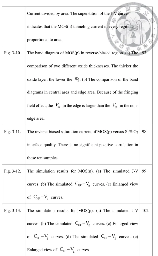
Fig. 1-1. The unusual currents shown in MOS(p) reverse-biased region.
Within the thickness range of 1.9~2.7 nm, the thicker the oxide layer, the larger the gate leak current, which is totally contrary to normal tunneling current. However, this abnormal
phenomenon disappears when oxide layer thickness is larger than 3nm.
10
Fig. 1-2. Fabricating process of ultrathin MOS structures. 10 Fig. 1-3. Schematic diagram of anodic oxidation method. 11 Fig. 1-4. Temperature profile of RTP system used in POA process. 11 Fig. 1-5 Side view of ultrathin MOS structure. 12 Fig. 1-6. Schematic diagram of initializing an 800
×
500 grids spacematrix in order to solve the potential in the gate fringing region.
12
Fig. 1-7. (a) The two elements model for leaky MOS structures. The Cp’ and Rp’ can be directly obtained by a single measurement of HP 4284. (b) The three elements model which add the Rs term as the series resistance. To find the value of the three elements,
13
two measurements under different AC frequencies are needed.
Fig. 2-1. The energy band diagram of the simulation case 1 in this work.
Because of the barrier confinement, there are quantized energy levels in the inversion region.
43
Fig. 2-2. Calculation results of cases 1 and 2 by Eqs. (2-5) ~ (2-8): (a)(b) Conduction band potential EC
( )
z and carrier concentration(z)
n versus position z. The EC
( )
z s solved by Poisson equation and the linear approximated surface potential V(z) arequite different in cases 1 and 2. (c)(d) The semi-classical results
( )
n3D z and the quantum-mechanical results n2D
( )
z (calculated by Eqs. (2-6) ~ (2-8)), and the inconsistency index of n3D( )
z /n2D( )
z in cases 1 and 2. The increasing trend of the inconsistency index points out inconsistency problem in 2D-3D transition region.45
Fig. 2-3. Calculation results of cases 1 and 2 by Eqs. (2-10) ~ (2-31):
(a)(b) Conduction band potential EC
( )
z and carrier concentration n(z) near the surface in cases 1 and 2. (c)(d) Thedifference between EC
( )
z solved by poisson equation and the potential approximated by Eq. (10a). (e)(f) The carrier48
inconsistency problem between semi-classical and quantum- mechanical (Eqs. (2-10) ~ (2-31)) calculations.
Fig. 2-4. The comparison between the wave functions of previous
researches (Airy function) and this work (Bessel function of the first kind, see Eq. (28)) in case 2.
49
Fig. 2-5. The comparison (not in proportion) between the 2D density of states g2D
( )
E and 3D density of states g3D( )
E . Since thequantized energy states
E
n becomes denser when E becomes higher, g2D( )
E is never going to converge to g3D( )
E in the 2D-3D transition region, and it is why the quantum-mechanical calculations in Sec. 2-1 and Sec. 2-2 cannot fix the inconsistency problem (see also Eqs. (32) ~ (34)).50
Fig. 2-6. (Not in proportion) (a) The comparison between different types of density of states in k-space: g3D
( )
E dE is a shell,( )
2D E E
g d is a ring, and g2D−3D
( )
E Ed has the shape between a ring and a shell. The blue shaded region (g2D−3D( )
E Ed ) is filled or partially filled because of the uncertainty of wavevector. (b) The concept of the filling rate function R(k). In 2D,
( )
R2D k is a delta function; in 3D, R3D
( )
k =1; in 2D-3D 52transition region R2D−3D
( )
k values from 0 ~ 1 and is proportional to Ψn( )
kz 2. In order to simplify the simulation,we let R2D−3D
( )
k =2 , ,
exp z z n
z n
k k k
−
− ∆
in this work. (c)
The quantized energy bands are broadened because of the uncertainty principle.
Fig. 2-7. Calculation results of cases 1 and 2 by using the uncertainty principle (UP) correction (Eqs. (2-38) ~ (2-45)): (a)(b) Conduction band potential EC
( )
z and carrier concentration(z)
n near the surface in cases 1 and 2. (c)(d) The difference between EC
( )
z solved by Poisson equation and the potential approximated by Eq. (2-10a). (e)(f) The carrier inconsistency between semi-classical and quantum-mechanical (Eqs. (2-38) ~ (2-45)) calculations. With the correction of uncertainty principle, the carrier inconsistency problem is solved.55
Fig. 2-8. The potential diagram of Case 2. Condition (2-10c) is still a simplified approximation of potential, but it’s well enough for us to solve the inconsistency problem.
56
Fig. 2-9. The calculation results for case 3 (hole accumulation) by using 58
the uncertainty principle (UP) correction. (a) Valence band bending and carrier concentration near the surface. (b) The difference between EV
( )
z solved by Poisson equation and the potential approximated by Eq. (2-10a). (c) 2D-3D carrier distribution and its comparison to semi-classical calculation.Unlike case 1 and case 2, the hole concentration is larger than the semi-classical result around 10nm ~ 20nm region (see Fig.
2-7). Also, carriers in case 3 have a wider distribution and a lower peak concentration than carriers in case 2. It is due to that hole has a longer wavelength than electron in Silicon.
Fig. 2-10. The result of the Fourier transform of Eq. (2-28). In this Figure, we use the 1st, 5th, and 10th eigen-states of case 2 as examples.
(a) Ψn
( )
z (b) F{
Ψn( )
z}
2. (c) The real and imagine components of Ψ10( )
kz . Note that Ψn( )
kz 2 =( ( ) )
2( ( ) )
2Re n kz Im n kz
Ψ + Ψ
(d) The results of Fourier transformation on partial region of Ψ10
( )
z . The region near to the Si/SiO2 interface is corresponding to the region with higher kinetic energy and momentum, and vice versa.60
Fig. 2-11. (Not in proportion) The energy-position diagram of case 2. 61
Electrons in position 1 have higher kinetic energy than electrons
in position 2, and the maximum kinetic energy is
( )
En−V z=0 . This helps to explain why
k
clmax,1>k
clmax,10>max,5
k
cl in Fig. 2-10(b). Also, the wave packet of each electron keeps moving back and forth between the interface and the potential barrier EC( )
z , which indicates that∆ z
n and,
k
z n∆
may be functions of z.Fig. 3-1. (a) MOS(p) J-V curves with different oxide layer thicknesses.
(b) MOS(n) J-V curves with different oxide layer thicknesses.
The arrows in both figures indicate the saturation voltages of reverse-biased current.
85
Fig. 3-2. The high and low AC frequencies’ C-V curves of ultrathin
MOS structures: (a)
C
HF− V
gof MOS(p) (b)
C
LF− V
g of MOS(p) (c)C
HF− V
gof MOS(n) (d)
C
LF− V
g of MOS(p).87
Fig. 3-3. The C-V curves of MOS structures in depletion regions. The arrows in (a) & (c) indicate the deep depletion phenomenon starting voltages in depletion regions. These arrows’ places are almost the same as the arrows in Fig. 3-1 (a) & (b).
89
Fig. 3-4. Simulated I-V and C-V curves for (a)(c) MOS(p) (b)(d)
MOS(n) structures with oxide thickness from 1.8 nm to 2.8 nm.
The simulation software is Atlas (ver. 5.18.3.R, 20/3/2012) of SILVACO Company.
91
Fig. 3-5. Using the quantization model in Chapter 2 with the
consideration of gate leakage current, we can solve the quasi- Fermi level near the surface.
92
Fig. 3-6. The modified Tsu-Esaki tunneling model in this study. 92
Fig. 3-7. Band diagram of ultrathin MOS(n) structure under different reverse-biased voltages.
93
Fig. 3-8. Band diagram of ultrathin MOS(p) structure under different forward-biased voltages.
94
Fig. 3-9. (a) MOS(p) tunneling Current divided by area. The superstition of the J-V curves indicates that the MOS(p) tunneling current in accumulation region is proportional to area. (b) MOS(p) tunneling current divided by perimeter. The superstition of the J-V curves indicates that the MOS(p) reverse-biased saturation current is proportional to perimeter. (c) MOS(n) tunneling
96
Current divided by area. The superstition of the J-V curves indicates that the MOS(n) tunneling current in every region is proportional to area.
Fig. 3-10. The band diagram of MOS(p) in reverse-biased region. (a) The comparison of two different oxide thicknesses. The thicker the
oxide layer, the lower the
Φ
B. (b) The comparison of the band diagrams in central area and edge area. Because of the fringingfield effect, the
V
ox in the edge is larger than theV
ox in the non- edge area.97
Fig. 3-11. The reverse-biased saturation current of MOS(p) versus Si/SiO2
interface quality. There is no significant positive correlation in these ten samples.
98
Fig. 3-12. The simulation results for MOS(n). (a) The simulated J-V curves. (b) The simulated
C
HF− V
g curves. (c) Enlarged view ofC
HF− V
g curves.99
Fig. 3-13. The simulation results for MOS(p). (a) The simulated J-V curves. (b) The simulated
C
HF− V
g curves. (c) Enlarged view ofC
HF− V
g curves. (d) The simulatedC
LF− V
g curves. (e) Enlarged view ofC
LF− V
g curves.102
Fig. 3-14. The
V
ox and current ratio Jt h,(
edge)
/Jt h,(
central)
near the edge of gate (the point x=0 is the edge of the gate). The current density at the edge is up to 5×1 07 times of the current density in the central area.102
Fig. 3-15. The J-V characteristics of (a) MOS(p) (b) MOS(n) in dark/
illuminated environment. The arrows in the figure are corresponding to the arrows in Fig. 3-16 and Fig. 3-17.
103
Fig. 3-16. The C-V characteristics of MOS(p) in: (a) dark environment (b) illuminated with 20 mW/cm2 light source (c) illuminated with 35 mW/cm2 light source (d) illuminated with 65 mW/cm2 light source.
105
Fig. 3-17. The C-V characteristics of MOS(n) in: (a) dark environment (b) illuminated with 20 mW/cm2 light source (c) illuminated with 40 mW/cm2 light source (d) illuminated with 65 mW/cm2 light source.
107
Fig. 3-18. Band diagram analysis for light induced hole tunneling current in MOS(p) reverse-biased region.
108
Fig. 3-19. (a) J-V curves (b) C-V curves of the fresh sample and the sample after 700s negative voltage stress.
109
Fig. 3-20. Band diagram analysis for long period gate injection current stress induced current lowering in reverse-biased region of MOS(p).
109
Fig. 4-1. The C-V characteristics for extremely leaky MOS structures. (a) MOS(p) (b) MOS(n)
115
Chapter 1 Introduction
1-1 Motivation 1-2 Experimental 1-3 Simulation Tools 1-4 Measurements
1-4-1 Capacitance Correction
1-4-2 Thickness of Oxide Layer
1-4-3 Interface Trap Density Extraction
1-1 Motivation
It’s been more than four decades that people found the unusual I-V characteristic of metal-oxide-semiconductor (MOS) structure with ultrathin oxide layer (thickness <
4 nm) in reverse-biased region [1]. It is unusual because of the thicker the oxide layer, the larger the reverse-biased current, which is contrary to the nature of normal tunneling
current. The gate metal in Ref. 1 is Au, and the substrate is n-type silicon with 1016 cm-
3 doping concentration. Also, in other researches, researchers found the same
phenomenon in MOS(p) structure with Al gate and 1015 cm-3~1016 cm-3 doping concentration [2-3], and we also found the same characteristics in our measurements (see Fig. 1-1). These previous researches tried to give possible explanations to the unusual I-V characteristics, but they didn’t give physical models which could quantitatively simulate the unusual I-V curves.
Thus, the motivation of this research is to find out a physically right model which can explain the both the I-V and C-V curves of the ultrathin MOS structure qualitatively and quantitatively.
1-2 Experimental
In this research, all of the ultrathin MOS samples (both MOS(p) and MOS(n)) are fabricated by the following process (see also Fig. 1-2, Table 1-1). First, the silicon substrates are cleaned by the stardard RCA process. The resistance of the silicon substrates are 1~10 Ω cm⋅ ; the dopant is boron for MOS(p) (equivalent doping
concentration
15 3
3 10 cm
−≈ ×
), and phosphor for MOS(n) (equivalent doping concentration15 3
1 10 cm
−≈ ×
).Second, we use the anodic oxidation (ANO) method [4-5] to grow the ultrathin
oxide layer. In the ANO process, we tilted the Pt electrode by an angle (18 ~ 20 ) in order to grow different thicknesses of oxide layer on a same substrate. The closest distance between the electrode and the substrate is around 0.5 cm (see Fig. 1-3).
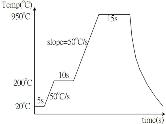
Third, a post-oxidation annealing (POA) process is applied to improve the quality of the oxide layer. We use a rapid thermal process (RTP) system to accomplish the annealing process. The temperature setting profile of RTP is shown in Fig. 1-4.
The fourth step to the sixth step are gate metal evaporation, photolithography, and back electrode metal evaporation. We use aluminum (work function around 4.1~4.28 eV, depending on crystal orientation of dielectric layer) as gate metal and back electrode. In the photolithography step, a negative photo resist and wet etching process is applied. The pattern of Al gate is square and its parameters are shown in Table 1-1.
The side view of finished MOS structure is shown in Fig. 1-5.
1-3 Simulation Tools
All the simulation in this work is done by using the programing software MATLAB, and the code is written by ourselves, which can be found in the Appendixes.
In the simulating process, one of the most important tasks is to solve the potential energy in space, i.e., to solve the Poisson equation:
2
0
V
r
ρ
∇ = −
ε ε
(1-1)Because the carrier distribution
ρ
in eq. (1-1) is complicated, usually it’s hard to find an analytical solution for Eq. (1-1). Thus, the most common way to solve to discretize the differential equation. For example, if we want to solve the 1D case of Eq. (1-1), the discretized form of (1-1) is:0
V(x h) V(x) V(x) V(x-h)
(x)
r
h h
h
ρ ε ε
+ − −
− = − (1-2)
where h is the length of the grid, and we let h=0.1 nm in our simulation. By iterating Eq. (1-2), we can get a converged solution for V(x).
Eq. (1-2) is the simplest example for the discretized Poisson equations, and it can be used to solve the potential profile in the non-fringing region of MOS structure.
In this research, in order to find out the potential profile in 2D space, we discretize the 2D space into several regions and set the grids with different sizes in different regions (see Fig. 1-6). Considering both precision and program efficiency, we set extremely small grid size in the regions which we want very precise information, and set a large grid size in the regions where data have a flat gradient to position. In Fig. 1-6, we initialize a space matrix with 800×500 grids in our simulation and distinguish the matrix into five regions. In region D, the grids are 0.1nm×1nm rectangular. Thus, the discretized Eq. (1-1) is
V(x h, y) V(x, y) V(x,y) V(x-h,y)
V(x, y 10h) V(x, y) V(x,y) V(x,y-10h)
(x, y)
10 10
10 Si
h h
h
h h
h
ρ ε
+ − −
−
+ − −
−
+ = −
(1-3)
Similarly, on the dividing line between regions D and E, the discretized Eq. (1-
1) is
V(x h, y) V(x, y) V(x,y) V(x-5.5h,y) 5.5
0.5 ( 5.5 )
V(x, y 10 h) V(x, y) V(x,y) V(x,y-10h)
(x, y)
10 10
10 Si
h h
h h
h h
h
ρ ε
+ − − −
× +
+ − −
−
+ = −
(1-4)
And the discretized Eq. (1-1) on the dividing line between regions C and D is
[ ] [ ]
[ ] [ ]
V(x h, y) V(x, y) V(x,y) V(x-0.5 ,y) 0.5
0.5 ( 0.5 )
V(x, y 10h) V(x, y) V(x,y) V(x,y-10h)
10 10 0
10
Si ox ox
ox ox
ox ox
d
h d
h d
h h
h
ε ε
ε ε
+ − −
−
× +
+ − −
−
+ =
(1-5)
where
d
oxis the thickness of the oxide layer. The right side of Eq. (1-5) is equal to 0 because quantum confinement effect of carriers makesρ(x, y)= 0 (we will explainmore about the quantum mechanical effect in Ch. 2).
Eq. (1-4) demonstrates how to calculate the discretized Poisson equation between different grid sizes, and Eq. (1-5) demonstrates how to calculate the discretized Poisson equation between two different materials. Thus, by sufficient iteration times, we can obtain the potential profile V(x,y) in Fig. 1-6.
1-4 Measurements
The capacitance-voltage (C-V) and current-voltage (I-V) characteristics are measured by HP 4284 RLC meter and HP 4140B pA meter respectively. However, the measured C-V curves need correction when the leakage current is large.
1-4-1 Capacitance Correction
The two equivalent circuit models are shown in Fig. 1-7 which try to extract the differential capacitance in a leaky MOS capacitor. In Fig. 1-7(a), the Cp’ and Rp’ can be directly calculated by the amplitude and the phase of impedance, which means a single measurement done by HP 4284 is enough to obtain the values of Cp’ and Rp’. In Fig. 1- 7(b), because of the added term Rs, two measurements under different AC frequency is needed to find the values of Cp, Rp, and Rs. The Cp can be calculated as [6]
(
12 1 22 2)
2 2 22 2 122 11 1 2 2
2 2
1 2
' ' ' '
'- ' 1
4 ' ' ' '
p
R C R C
f C f C
R C R C
C f f
π
−
+
= − (1-6)
However, the three-element model is improved by some following researches [7-8]. Also, in our measurements, we find that the larger the area of the top gate, the more inaccurate the method (see Table 1-2). Some research added the lateral resistance into consideration [7]. Other modified the model and even added an inductance element to a five-element model [8]. In our opinion, we consider the inaccuracy of two frequency correction may origin from the non-linearity of the I-V characteristic of MOS
capacitor. Namely, outside a certain range, the linear model in Fig. 1-7(b) may not be right. A possible equation of the non-linear impedance is:
1 R exp
s p
p
V q V
Z R
I j C
ω
nkT
∆ ∆
= ∆ = +
(1-8)
where n is around 7.5~8.5 in the accumulation region of Fig. 1-1. However, the non- linear Eq. (1-8) is problematic when we try to use it in capacitance correction. Thus, in the measurements, we measure as least three frequencies and use different frequency pairs to check the consistency of the corrected capacitance. If the consistency is checked, than we can confirm the two frequency correnctino method is still effective to the C-V data.
1-4-2 Thickness of Oxide Layer
After the C-V correction in 1-4-1, we can use the differential capacitance in the accumulation region to fit the theoretical C-V curves, and then find out the thickness of the oxide layer. The theoretical C-V curves are obtained by previous researches [9-10]
which considered the quantum mechanical effects in MOS structure. The fitting method is using the least squares method to decide what thickness is the best fitting. The fitting range of the C-V curves for are -1.1~ -1.8 (V) for MOS(p) and 0~ 0.8(V) MOS(n).
1-4-3 Interface Trap Density Extraction
The combined high-low frequency method [11] is used to extract the interface trap density Dit in this work. We calculate the interface trap induced capacitance Cit by
1 1
1 1 1 1
( ) ( )
it it
LF ox HF ox
C qD
C C C C
− −
= = − + − (1-7)
where the
C
ox is the saturated capacitance in accumulation region. TheC
LF is the C-V curves measured by a low frequency AC small signal, which is low enough to let every interface states contribute to interface trap induced capacitance. On the contrary, theC
HF is measured by a high enough frequency signal to let no charges in interface states in or out during the small signal cycles.Table 1-1. The parameters and method used in fabricating process.
Structure MOS(p) MOS(n)
Wafer cleaning Standard RCA
Oxide layer growth ANO: 15V, 7 mins, tilted angle 18 ~ 20 , closest distance between electrode and sub substrate is 0.5 cm.
RTA N2, 20 torr, 20℃(5s) 200℃(10s) 950℃(15s) Temperature ascending slope: 50℃/s
Gate metal Aluminum, 300 nm
Gate pattern Square: 1 5 0×1 5 0 , 3 0 0×3 0 0 , 6 0 0×6 0 0 (µm)2
Back electrode Aluminum, 300 nm
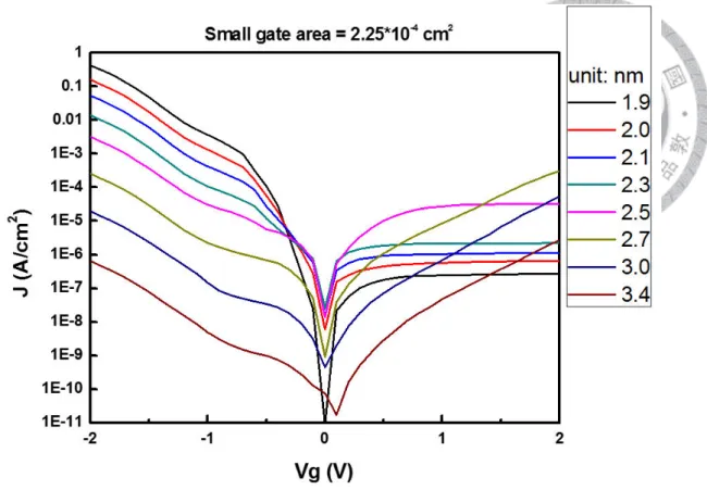
Table 1-2. The failed of two frequency correction method is large area topgate cases.
Correction frequency pair
Thickness fitting for Small gate
Thickness fitting for Medium gate
Thickness fitting for Large gate Sample
A
100k/1m 1.9 (nm) 1.7 (nm) 1.0 (nm)
10k/100k 2.0 (nm) 2.05 (nm) 2.05 (nm)
Sample B
100k/1m 2.4 (nm) 2.2 (nm) 1.3 (nm)
10k/100k 2.55 (nm) 2.55 (nm) 2.6 (nm)
Fig. 1-1. The unusual currents shown in MOS(p) reverse-biased region. Within the thickness range of 1.9~2.7 nm, the thicker the oxide layer, the larger the gate leak current, which is totally contrary to normal tunneling current. However, this abnormal phenomenon disappears when oxide layer thickness is larger than 3nm.
Fig. 1-2. Fabricating process of ultrathin MOS structures.
RCA wafer
cleaning Anodic Oxidation Post-Oxidation Annealing
Al gate
Evaporation Photolithography Back Electrode (Al)
Evaporation
Fig. 1-3. Schematic diagram of anodic oxidation method.
Fig. 1-4. Temperature profile of RTP system used in POA process.
Fig. 1-5 Side view of ultrathin MOS structure.
Fig. 1-6. Schematic diagram of initializing an 800×500 grids space matrix in order to solve the potential in the gate fringing region.
Fig. 1-7. (a) The two elements model for leaky MOS structures. The Cp’ and Rp’ can be directly obtained by a single measurement of HP 4284. (b) The three elements model which add the Rs term as the series resistance. To find the value of the three elements, two measurements under different AC frequencies are needed.
Chapter 2
Theory of Quantization Effects in MOS Accumulation and Strong Inversion Layer
2-1 Introduction and Problems with Previous Researches
2-2 An Exponential Surface Potential Approximation Approach
2-3 Theory of Density of States with Uncertainty Principle Correction
2-4 Discussion
2-4-1 Simplifications Used in the Simulations
2-4-2 Applying the Method to Hole Accumulation Case
2-4-3 The Solution of the Inconsistency Problem in Previous Researches
2-4-4 The Validation of Some Assumptions Used in This Work
2-1 Introduction and Problems with Previous Researches
When MOS or MIS (metal-insulator-semiconductor) structures are in accumulation (n-type substrate) or strong inversion (p-type substrate) region, there are
electrons of high concentration near the surface of insulator layer. Because of the barrier confinement of the high barrier potential of insulator and the semiconductor bending potential (see Fig. 2-1), these electrons are only allowed to exist in quantized energy levels rather than continuous energy band. In order to find out the carrier distribution in the accumulation or the strong inversion layer, it’s necessary to solve the wave function and its eigenvalues of energy. Thus, we should solve the Schrödinger’s equation (2-1) for wave function and the Poisson’s equation (2-2) for potential function:
2 2
(z) 2
(E V(z)) 0
n z
n n
d m
dz
Ψ + − Ψ =
ℏ
(2-1)2 2
(z) (z)
s
d V dz
ρ
= − ε (2-2)
However, the two second-order differential equations above are almost impossible to be solved simultaneously and to obtain analytical solutions because combining them together makes a non-linear four-order differential equation.
An alternative numerical method of solving these equations is Poisson- Schrödinger iteration [12]. First, solve the potential function (2-2) by using the well- known semi-classical formula (2-3) for carrier distribution to generate a possible initial solution:
0
(z) N 2
C 1 n d
eζ χ
ζ ζ π
∞
= × × −
∫
+ , (2-3) whereζ = − (E E ) / kT
C , andχ = (E
F− E ) / kT
C .The relation between n(z) and ρ(z) in Eq. (2-2) is:
(z) q[n(z) p(z) N
DN ]
Aρ =− − − +
(2-4)where q is the elementary charge. Second, in order to solve
Ψ
n(z)
andE
n more easily, we approximate the function V(z) in Eq. (2-1) to some special form. Some previous researches [13-17] assumed the V(z) has the a linear form in semiconductor:V(z)=qξz, if z>0 (2-5a) V (z)= ∞, if z ≤0, (2-5b) where ξ is the surface electric field considered as a constant when nearing the
semiconductor surface to insulator. Then, because in z-direction the electrons are confined in the well, some previous studies suggested considering it as a 2D electron gas (2DEG) system and using the density of states of 2D cases [13-17]:
g(E) mt2
=π
ℏ , (2-6) where mt = m mx y is the transverse mass; Eq. (2-6) already includes the factor of
two spin directions of electrons. Thus, it could be derived that [13,15]:
1/3 2 2
2 2
(z) t ln 1 exp F n Cn z n 2 z
n
m kT E E E m q
n Ai
kT q
ξ
π ξ
−
= ℏ
∑
+ × − ℏ (2-7)2/3 1/3 1
(q )
, 1, 2, ...
(2 m )
n n
z
E ξ s n
= − ℏ − =
, (2-8)
where
C
n is the normalization constant forΨ
n, Ai represents for Airy function, ands
n stands for the nth root for Ai(s)=0.After obtaining the new distribution of electrons from Eq. (2-7), apply it into Eqs. (2-2) and (2-4) to solve the real shape of V(z). Then, find the best fit of the new V(z) in the form of Eq. (2-5a) and solve Eq. (2-1) again to get a new electron distribution. Keep iterating this Poisson-Schrödinger solving loops unless the results pass the check of convergence. Applying the values of parameters in Table 2-1, we obtain the results as shown in Fig. 2-2.
In Fig. 2-2, it shows that there are two major problems of the calculation based on the method above: 1. No matter how we choose the value of the “constant electric field”, the real shape of V(z) is not linear even within a small range (10nm) from the insulator-semiconductor surface, which means the assumption of linear V(z) causes
non-negligible errors. 2. In Fig. 2-2(b), we define the ratio
n
3D(z)/ n (z)
2D as the inconsistency index. Then
2D(z)
is obtained by Eq. (7), and then
3D(z)
is calculated by Eq. (2-3) under the same band bending, i.e. using theE (z)
C solved by Eq. (2-2) in Fig. 2-2(a). The further the index deviated from 1, the worse the consistency. Logically speaking, because the n(z) is a continuous function, the inconsistency index shouldapproach to 1 when z becomes larger. However, as shown in Fig. 2(c) and Fig. 2(d), the electrons distribution has an extremely bad consistency in the 2D to 3D transition region. The
n
2D(z)
even has a difference of several orders fromn
3D(z)
in the transition region, and this difference becomes larger when z becomes larger.2-2 An Exponential Surface Potential Approximation Approach
To resolve the problems above, we must abandon the unreasonable assumption that “the electric field is a constant when nearing the semiconductor surface to insulator”. Eq. (2-2) can also be written in the form:
(z) (z)
s
d dz
ξ ρ
=
ε
(2-9)which suggests that after the peak of n(z) (around z≈0.7 nm), the constant electric
field assumption is invalid. Since the range of validation is less than 1nm, the linear approximation method is only useful in finding the first quantization energy levels.
Therefore, we propose a much better approximation function for surface potential:
V(z) V 1 exp0 z q z, if z 0
A ξ
= − − + > (2-10a)
V (z)= ∞, if z ≤0 (2- 10b)
V(z) V 1 exp0 z , if 0 z 10 nm A
≈ − − < < (2-10c)
V(z) V q z, if z 10nm = +
0ξ >
, (2-10d) whereV
0, ξ and A are the fitting parameters. The parameter A is about 2nm ~ 4nm.Because of Fermi-Dirac distribution, the first few states determine most of the
electrons’ positions in inversion or accumulation region, which means that obtaining
the accurate energy levels of the first few states is crucial. Also, in Eq. (2-1), if the
n
(z)
Ψ
is only non-zero in the range of 0 ~ 10 nm (see Fig. 2-4), then we can apply condition (2-10c) in Eq. (2-1) and let2 2
0 0 0
2 2
2 2
(V E ), V , exp
2
z z
n n
m m z
t k
γ
A= − = = −
ℏ ℏ (2-11) and use the relationship
2 2
2 2 2 2 2
2 2, 2, 2 2 2
4 4
d d d d d d d
dz A dz A dz dz d dz d
γ γ γ γ γ γ
γ γ
Ψ Ψ Ψ
= = = + (2-12)
Eq. (2-1) becomes
( )
2 2
2 2 2
2 2 2 0
(z) (z)
(z) 0
4 4
n n
n n
d d
t k
A d A d
γ γ γ
γ γ
Ψ Ψ
+ + − + Ψ = (2-13)
Divide Eq. (2-13) by
2
4 A
2γ
, and let0 0
2 2 exp
2 k A k A z
κ
=γ
= − A (2-14) Eq. (2-13) becomes
2 2
2 2
( ) 1 ( ) 4
1 ( ) 0
n n n
n
d d At
d d
κ κ
κ κ γ κ κ
Ψ Ψ
+ + − Ψ =
(2-15) To solve Eq. (2-15), we use the two following boundary conditions:
0 20
(z) | 0 ( ) | 0
n z= n
κ
κ=k AΨ = ⇔ Ψ =
(2-16a)(z)| 0 ( )|
00
n z=∞ n
κ
κ=Ψ = ⇔ Ψ =
(2-16b) The solution to Eq. (2-15) is a Bessel function [18]:( ) ( )
1 2 2 2
( ) n n
n
κ
c J−t Aκ
c J t Aκ
Ψ = + (2-17)
Consider the boundary condition (2-16a), the relation between c1 and c2 can be found
as:
( )
( )
2 0
1
2 2 0
2 2
n
n
t A t A
J k A
c
c = − J− k A (2-18) We can choose
( ) ( )
1 2 2 0 , 2 2 2 0
n n
t A t A
c =J k A c = −J− k A (2-19) Consider the boundary condition (2-16b) and use the following polynomial expansion
of Bessel function [18]:
( ) ( )
( )
0
1
! 1 2
m v m
v
m
J z
m v m
κ
∞ +
=
−
=
∑
Γ + + (2-20)when z→ ∞
( κ
→0)
, the asymptotic function of Eq. (2-17) can be written as:( ) ( )
( ) ( )
( )
2 2
0 2 0 2 0
1 1
| 2 2
2 1 2 2 1 2
n n
n n
t A t A
n t A t A
n n
J k A J k A
t A t A
κ
κ κ
κ
−
→ −
Ψ = Γ − + − Γ +
(2-21)
Use Eq. (2-14) to replace κ with z:
( ) ( ) ( ) ( ) ( )
2 2
0 0
2 0 2 0
| 2 2
2 1 2 1
n n
n n
n n
t A t A
t z t z
n z t A t A
n n
k A k A
z J k A e J k A e
t A t A
− −
→∞ −
Ψ = −
Γ − + Γ + (2-22)
The coefficient of et zn in Eq. (2-22) must be zero. There are two possible solutions:
( )
1 0
2t An 1 =
Γ − + (2-23a)
( )
2 2 0 0
t An
J k A = (2-23b) Solution (2-23a) requires
2 t A
n1 0, n 0,1,2,3,...
− + = =
(2-24)which makes Eq. (2-17) become
( )
1(
2 0)
( 1)( )
( 1)(
2 0)
1( )
0n
κ
Jn+ k A J− +nκ
J− +n k A Jn+κ
Ψ = + = (2-25)
Because when n is an integer, the Bessel function has the relation [18]:
( ) ( )
1( )
1 1n ( 1)
n n
J + x = − + J− + x (2-26)
Thus, solution (2-23a) cannot be the answer, which indicates Eq. (2-23b) is the only
possible answer.
The way to find out all possible
t
n in Eq. (2-23b) is using program and let2
nv = t A =
discrete values from2k A
0 to 0, and use the interpolation method to find out allt
n which makes 2(
2 0)
0t An
J k A = . Then assign those values to
t
0,t
1,…,t
n in a descending order. Using the relation in Eq. (2-11), we can find that:2 2
E V0 , 1, 2,...
2
n n
z
t n
= −ℏm =
(2-27)
By using the programming software MATLAB, the values to all
E
n can be found within 0.01 second.Since
c
1= 0
, we can rewrite the unnormalized wave function as:( )
2 2 0 exp 2n t An
z J k A z
A
Ψ = − (2-28)
and let
N
n be the normalized coefficient. Use the normalization condition:( ) ( )
0
2 0 2
0 2
2 1
n n n k A n
N z dz N κ Adκ
κ
∞ Ψ = Ψ − =
∫ ∫
(2-29)2
Nn can be found as:
( )
0
0 2 1
2 2
2
n k A n
N κ Adκ
κ
− −
=
∫
Ψ (2-30)Assume the use of 2D system’s density of states, i.e., Eq. (2-6), is valid, we can derive
(z)
n under the exponential surface potential approximation by simulating Eq. (2-7) as:
2 2
2 0
(z) 2 ln 1 exp 2 exp
2
n
t F n
n t A
n
m kT E E z
n N J k A
kT A
π
−
= ℏ
∑
+ × − (2-31a)Although condition (2-10c) can help us to find values for the first three or first
four energy states of acceptable accuracy, we still need condition (2-10d) to solve the
higher states. Thus, the old method in Eqs. (2-5) ~ (2-8) is useful again (Eq. (2-10d)
and Eq. (2-5) only differ by a constant.). Note: 1. Since the nth state has n peaks for
( )
2n z
Ψ , the number n of the Ψn
( )
z solved by Eq. (2-10d) should start with the state which has one more peak than the last state solved by Eq. (2-10c). 2. The Ψn( )
z solved by applying (2-10d) in Eq. (1) is not accurate in the range of 0 ~ 10nm from thesurface, but would be a good approximation for z > 20nm. Therefore, we rewrite Eq.
(2-31a) as:
2 2
2 0
2
1/3 2 2
2
(z) { ln 1 exp 2 exp
2
ln 1 exp C z 2 }
n
t F n
n t A
n b
F n n z
n n b
m kT E E z
n N J k A
kT A
E E E m q
kT Ai q
π
ξ ξ
≤
>
−
= + × −
−
+ + × −
∑
∑
ℏ
ℏ
(2-31b)
where b is the number of states obtained by using condition (2-10c).
In Fig. 2-3 and Table. 2-2, we can find that the new approximation method
makes the values of
E
n more reasonable i.e.,E
n become denser and∆ E
n become smaller while n becomes larger. Also, the difference between real potential andapproximated potential is much lesser than the old method.
In Fig. 2-4, we can see the comparison between the wave functions of previous
researches (Airy function) and this work (Bessel function of the first kind, see Eq. (2-
28)). Although the functions’ forms are different, the shapes of them are similar. The
difference of the distributed range of 4th-state wave functions between previous work
and this work is due to the difference of the approximated potentials (see Fig. 2-2(b)
and Fig. 2-3(b)); obviously, our approximation method is better than previous work.
Also, the wave functions of the first few states is almost confined within 10nm from
surface, which shows the validity of using condition (2-10c) in Eq. (2-1).
Although the problem of the potential approximation is solved, the inconsistency problem of n(z) in the 2D-3D transition region is still not fixed (see Fig.
2-3(e) and Fig. 2-3(f)). The cause of such simulation results is that the relation between
energy (E) and density of states in 2D system (denoted as
g (E)
2D ) is [13,14]:2 2
g (E)
D t(E E )
nn
m U
= π ℏ × ∑ −
, (2-32) where U(x) is the unit step function:( ) ( )
1, if 0 0, if 0
U x x
U x x
= ≥
= < (2-33) However, the relation between energy and density of states in 3D system (denoted as
g (E)
3D ) is(
*)
3 / 2( )
1/ 23 2 3
g (E) 2 E E
2
e
D C
m
= π −
ℏ (2-34) Since
E
n becomes denser when E becomes higher, Eq. (2-32) is never going to converge to Eq. (2-34) in the 2D-3D transition region (See Fig. 2-5).2-3 Theory of Density of States with Uncertainty Principle Correction
The inconsistency problem indicates that the assumption of using the density of
states of 2D system is not valid for the so-called “2DEG” system in our cases. It doesn’t
mean that the quantization of energy will not happen, but means that we need to modify
the theory of calculating density of states in such cases. In this part, we present a time
efficient way to estimate the real relation between energy and density of states by using
the uncertainty principle.
The uncertainty principle states that the standard deviation of position
∆ z
nand the standard deviation of momentum
∆ p
z n, has the following relation:, ,
, 1
2 2
n z n n z n
z p or z k
∆ ∆ ≥ ℏ ∆ ∆ ≥
(2-35)
where ∆kz n, =