國立臺灣大學電機資訊學院電子工程學研究所 碩士論文
Graduate Institute of Electronics Engineering College of Electrical Engineering & Computer Science
National Taiwan University Master Thesis
低功耗三角積分時間至數位轉換器
Delta-Sigma Time-to-Digital Converters for Low Power Applications
張智凱 Chih-Kai Chang
指導教授:呂良鴻 博士 Advisor: Liang-Hung Lu, Ph.D.
中華民國 105 年 7 月
July, 2016
致謝
本論文的完成,首先要感謝呂良鴻教授的悉心指導,感謝老師對我研究所花 的精力與時間,老師對於研究嚴謹的要求,更使我能在研究上能深入探索,透過 多次討論逐漸修正論文方向,使得本論文能夠完整呈現。
感謝論文口試委員中央大學的邱煥凱教授、交通大學的郭建男教授能夠撥冗 於論文口試時給予寶貴的意見,您們提出的批判與建議使得論文內容能更加完備。
感謝國家晶片系統設計中心提供的晶片實作、教育訓練以及量測服務,以及 所有工程師與講師的協助與指導。
感謝台大電子所ADSI 實驗室全體成員,博班的煥昇、易耕、博智、博軒、渝
楷學長們不時地給予我研究上的建議以及幫助,帶我順利熟悉研究生活;碩班學 長弘鈺、瑋倫、沛耕、律文、浩然,以及志鴻、其穎、林森、家維、裕豐,與你 們在實驗室一起討論、研究的過程都讓我受益良多。
我要謝謝我的父母與家人們的栽培及鼓勵,沒有你們的支持,我無法完成我 的學業,也謝謝嘉逸在這段時間精神上的支持。
摘要
此論文中闡述了低功耗的三角積分時間至數位轉換器的設計技巧,以時間暫
存器來傳遞時域的量化誤差來達到高解析度的時間至數位轉換器。利用 90-nm
CMOS 製程,所提出的一階三角積分時間至數位轉換器,操作在 0.3 伏特的情況
下,晶片功耗為1.5 微瓦,並且在 50k 赫茲的頻寬內有效位元數(ENOB)為 10.9 位
元。此外,進一步利用相同的設計技巧實現二階的三角積分時間至數位轉換器,
並以此時間至數位轉換器應用至電容式感測器介面電路,操作在 0.6 伏特的情況
下,晶片功耗為11 微瓦,此電容式感測器介面電路輸入電容範圍為 0~5 皮法拉,
並在2k 赫茲的頻寬內效位元數(ENOB)為 9.8 位元。
Abstract
The thesis presents low power design techniques for delta-sigma time-to-digital (TDC) converters. By using time register to transfer the time-domain quantization error, the resolution of the TDC can be improved due to noise-shaping of the quantization error.
Fabricated in 90-nm CMOS, the first-order delta-sigma TDC consumes a current of 5
A from a 0.3-V supply. The circuit demonstrates an equivalent number of bits (ENOB) of 10.9 bits in 50 kHz signal bandwidth. Moreover, a capacitance-to-digital (CDC) converter with a second-order delta-sigma TDC is also presented. Consuming 18.4 A from a 0.6-V supply, the second-order CDC achieves an ENOB of 9.8 bits in 2 kHz signal bandwidth with an input capacitance range of 5 pF.
Contents
致謝 ... i
摘要 ... vii
Abstract ... ix
Contents ... xi
List of Figure ... xiv
List of Tables ... xvii
Chapter 1 Introduction ... 1
1.1 Motivation ... 1
1.2 Thesis organization ... 2
Chapter 2 Background ... 3
2.1 Applications ... 3
2.2 Performance metrics of TDC ... 6
2.2.1 Static performance ... 6
2.2.2 Dynamics performance ... 7
2.2.3 Counting rate and dead time ... 9
2.3 General TDC architecture ... 10
2.4 Delta-sigma TDC ... 16
Chapter 3 A Noise-Shaping Time-to-Digital Converter with Gated-Free Ring Oscillator ... 24
3.1 Introduction ... 24
3.2 Proposed delta-sigma TDC ... 25
3.2.1 Conventional gated ring oscillator TDC ... 25
3.2.2 Proposed delta-sigma TDC ... 27
3.3 Circuit implementation ... 29
3.3.1 Time Register ... 29
3.3.2 Leakage Suppression Switches ... 30
3.3.3 Gated-free ring oscillator ... 31
3.3.4 Noise analysis ... 32
3.4 Experimental Results ... 35
3.4.1 Measurement at 0.3-V supply voltage ... 35
3.4.2 Measurement at 0.6-V supply voltage ... 39
3.5 Conclusion ... 43
Chapter 4 Time-Mode Capacitive Sensor Interface with Second-Order Time-to-Digital Converter ... 45
4.1 Introduction ... 45
4.2 Proposed capacitance-to-digital converter ... 47
4.2.1 1-1 MASH TDC ... 47
4.2.2 Proposed second-order TDC ... 50
4.2.3 Capacitance-to-time converter ... 53
4.3 Circuit implementation ... 55
4.3.1 Gated switched-ring oscillator ... 55
4.3.2 Quantization error generator ... 56
4.3.3 Gate-delay buffers ... 57
4.4 Experimental Results ... 60
4.5 Conclusion ... 64
Chapter 5 Conclusion ... 65
Reference ... 67
List of Figure
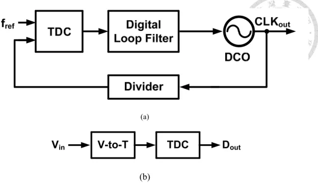
Fig. 2.1. (a) General architecture of ADPLL (b) and time-mode ADC. ... 4
Fig. 2.2. Quantization characteristic of the TDC. ... 7
Fig. 2.3. Timing figure of the time-to-digital conversion. ... 9
Fig. 2.4. (a)Conventional delay-line-based TDC and (b) Vernier type delay-line-based TDC. ... 10
Fig. 2.5. (a) SR latch followed by an XOR with its timing diagram and (b) the relationship between the delay time of SR latch and the input time difference. .... 12
Fig. 2.6. (a)Concept of a TA (b) and input/output transfer curve of a TA ... 13
Fig. 2.7. Conceptual timing diagram of a 3-bit CTDSA. ... 14
Fig. 2.8. Continuous time measurement of the interval. ... 16
Fig. 2.9. Discrete time measurement of the time interval... 16
Fig. 2.10. Schematic of GRO and its transient operation. ... 17
Fig. 2.11. Architecture of the GRO-TDC. ... 18
Fig. 2.12. Illustration of noise shaping in the discrete time measurement. ... 19
Fig. 2.13. Operation of the SRO-TDC... 20
Fig. 2.14. Leakage induced timing skew error in GRO. ... 20
Fig. 2.15. Simulation results of the TDC effective resolution. ... 21
Fig. 3.1. (a)The simplified block diagram and (b) the timing diagram of the GRO-TDC. ... 25 Fig. 3.2. (a) The architecture of the proposed TDC and (b) its conceptual timing
Fig. 3.3. Block diagram of the time register. ... 29
Fig. 3.4. Transient operation of the time register. ... 30
Fig. 3.5. Schematics of the leakage suppression switches... 31
Fig. 3.6. Schematic of the gated-free ring oscillator ... 32
Fig. 3.7. Simulated output spectrum of the TDC. ... 33
Fig. 3.8. Chip photo. ... 35
Fig. 3.9 Measured (a) DC transfer curve and (b) corresponding INL at 0.3-V supply. .. 36
Fig. 3.10 Measured PSD for a 885-Hz input at 0.3-V supply. ... 37
Fig. 3.11 Schematic of input-delay lines. ... 37
Fig. 3.12 Measured single-shot precision of the prototype TDC at 0.3-V supply. ... 38
Fig. 3.13 Measured (a) DC transfer curve and (b) corresponding INL at 0.6V-supply. . 39
Fig. 3.14 Measured PSD for a 22.6-kHz input at 0.6-V supply.. ... 40
Fig. 3.15 Measured single-shot precision of the prototype TDC at 0.6-V supply. ... 41
Fig. 4.1. Time-mode capacitance-to-digital converter. ... 47
Fig. 4.2. Simplified block diagram of the 1-1 MASH TDC. ... 47
Fig. 4.3. Timing diagram of the 1-1 MASH TDC. ... 48
Fig. 4.4. Proposed second-order TDC. ... 51
Fig. 4.5. Timing diagram of the proposed TDC... 52
Fig. 4.6. (a) Capacitance-to-time converter and (b) its timing diagram. ... 53
Fig. 4.7. Gated switched-ring oscillator. ... 55
Fig. 4.8. Quantization error generator. ... 56
Fig. 4.9. (a) Gated-delay buffer unit and its timing diagram (b) without and (c) with delay cell To. ... 57
Fig. 4.10. Circuits schematic of the proposed error feedback structure. ... 58
Fig. 4.11. Chip photo. ... 60
Fig. 4.12. Output spectrum with 3pF input. ... 61 Fig. 4.13. Measured RMS noise of the CDC. ... 62 Fig. 4.14. Linearity test setup ... 62
List of Tables
Table 3-1 TDCPERFORMANCE AND COMPARISON WITH STATE-OF-THE-ART. ... 41 Table 4-1 COMPARE WITH STATE-OF-THE-ART ... 63
Chapter 1
Introduction
1.1 Motivation
In recent years, CMOS has become more attractive due to its low cost in volume and inherent capability in high level integration. Since the progress of CMOS process is driven by the digital circuits, the device size decreases in advance CMOS technology.
This progress results in a reduction of the transistor gate-oxide thickness, thus, lower operation voltage of the transistors. Due to the lower operation voltage, the intrinsic gain of a single transistor becomes lower and so as the input voltage range. As a result, the analog design becomes more challenge in nanotechnology.
To lower the design challenge of the analog design, digital-assisted analog design becomes more important. Therefore, time-mode signal processing (TMSP) gains more interest. Using TMSP, conventional representation of the signal in voltage domain is replaced by representation of the signal in time domain. Thus, the signal is represented by the time difference between two signal rising edge. Exploiting the time-mode operation, many power-hungry and large area analog circuits can be replaced by digital circuits. On the other hand, layout of highly digital circuits can be automatically generated by digital synthesis. Therefore, various architecture of the time-to-digital
converters have been published to accomplished a more energy efficient and cost effective system. Since the gate delay increases as supply voltage decreases, the resolution of a conventional delay-line based TDC is proportional to the supply voltage.
A higher supply voltage is needed to enhance the resolution of a delay-line based TDC which results in higher power consumption. Other approaches such as successive approximation (SAR) and two-step TDC have published to achieve higher resolution without raising the supply voltage. However, complex calibration is needed to overcome the PVT variation and process mismatch because of analog parameter dependency of these TDC. In addition to these TDCs, TDC paves a way to achieve sub-gate delay resolution without calibration. Several TDC has been published to achieve more energy efficient TDC. In this thesis, TDC design techniques are proposed to enhance the TDC performance and a capacitance-to-digital converter (CDC) is fabricated with a proposed second-order TDC using the proposed techniques.
1.2 Thesis organization
This thesis is organized as follows. In Chapter 2, the background of the TDC, and several prior arts of the TDC circuits with an emphasis on TDC is provided. In Chapter 3, a noise-shaping TDC with gated-ring oscillator is presented. By exploiting gated-free operation, the timing error associated with charge injection and leakage from the oscillator can be reduced. As a result, the proposed architecture achieves higher resolution in low power design. Based-on Chapter 3, a capacitance-to-digital converter with a low power second-order TDC is proposed in Chapter 4. Finally, a conclusion is provided in the Chapter 5.
Chapter 2
Background
2.1 Applications
Time-to-digital converter (TDC) has been used in a wide variety applications such as all-digital phase-locked loops (ADPLL), biomedical imaging time-of-flight (ToF) positron emission tomography (PET), fluorescence life time imaging microscopy (FLIM) and ToF range finding.
In biomedical imaging or range finding applications, TDC often integrated with single-photo avalanche diode (SPAD). For PET application, the TDC is used to detect two gamma rays from the annihilation events that happened in a patient’s body.
Detecting the time difference between the two gamma rays to analysis the location of the emission, the TDC resolution directly impact the signal-to-noise ratio (SNR) of the image.
Another important application for the TDC is FLIM. In this application, the TDC detects the decay time of the fluorophore. One can obtaine the chemical or physical properties depending on the lifetime of the fluorophore. In general, the lifetime of fluorophore ranging from nanosecond to millisecond. However, the fluorophore lifetime is sensitive to environment interference and is decreased by the interference. Therefore, the typical TDC for FLIM application is designed to have about 50 ps resolution with
50 ns dynamic range. Moreover, since the deadtime of the SPAD is reduced to nanosecond. The deadtime of the TDC becomes the main issue in the FLIM application.
The TDC also plays an important role in ADPLL since it can replace the traditional analog intensive phase detector and charge pump as shown in Fig 2.1 (a). The highly digital architecture can simplify the design complexity of the circuits in advance CMOS technology and can utilize digital loop filter instead of the area consuming RC loop filter. The programmability of the loop parameter is also an attractive advantage for the ADPLL design. In the ADPLL application, the trend for the TDC is to achieve high resolution since the resolution of the TDC dominates the in-band phase noise of the ADPLL. The single-sided noise power spectral density STDC is givn by
refref
π out tdc
TDC π
ref
2π sin ( ) 2
2 f 2
f f
f
S f f
f 12
(2.1.1)
where fref is the reference frequency, fout the ADPLL output frequency, and τtdc the TDC resolution. The TDC should have large dynamic range to detect large phase error.
In recent years, time mode signal processing (TMSP) also gains more interest because
(a)
V-to-T TDC
V
inD
out(b)
Fig. 2.1. (a) General architecture of ADPLL (b) and time-mode ADC.
of the difficulties in design analog circuits at low operation voltage. Fig 2.1 (b) shows an example of time-mode analog-to-digital converter which is composed of a voltage-to-time converter and a time-to-digital converter.
2.2 Performance metrics of TDC 2.2.1 Static performance
The static input-output behavior of an ideal TDC is given by a quantization characteristic as shown in Fig 2.2. The term quantization characteristic means that a continuous time inputs being mapped to the digital words. The step width of the quantization characteristic (TLSB) is the least significant bit (LSB) of a TDC, which means the range of the time interval being mapped to a single digital word. Different from an ideal TDC that the first step occurs at the position T00…01 = TLSB, the first step and the complete characteristic of a practical TDC might be shifted along the time axis.
The converter is said to have an offset error if the characteristic is shifted. In general, the gain of a ideal TDC kTDC is the steepness of the quantization characteristic which shown as the slope of the dot line in Fig 2.2. For a practical TDC, the gain may be varied from its ideal value. The variation of the gain is quantified by the gain error Egain, which can be expressed as
gain 11...11 00...01
LSB
1 ( ) (2N 2).
E T T
T
(2.2.1)It should be noted that the offset and gain error of the converter can be modeled by an additive or multiplicative term to the input time interval, so those errors do not cause non-linear distortion.
Non-linear imperfection in a TDC is its deviation of the quantization characteristic from its ideal shape and can be specified through the differential nonlinearity (DNL) and the integral nonlinearity (INL). DNL is defined as the difference between the actual and the ideal step widths in the quantization characteristic The INL is a macroscopic description of the arching of the quantization characteristic which defined as the
deviation of the step position from its ideal value normalized to one TLSB. The ideal value is defined by a straight line that can be a line connecting the first and the last step or a best fit line. Usually, DNL and INL are normalized to one TLSB.
2.2.2 Dynamics performance
For the static performance of the converter multiple measurement are average thus that any noise can be removed from the measurement results. For practical use, the noise can’t be neglected and reduces the effective resolution. For classical analog-to-digital converter, the dynamics performance is verified by applying a sinusoidal signal and evaluating the output spectrum. The resulting spectrum contains a peak at signal frequency and smaller peaks at multiples of the signal frequency and a noise floor. The smaller peaks are cause by the non-linear imperfections of the converter and the noise floor results from both quantization and physical noise. The signal-to-noise-and-distortion ratio is (SNDR) defined by
1/4 2/4 3/4 1 T
inT
refD
out00 0 01 10
11 T
LSBFig. 2.2. Quantization characteristic of the TDC.
signal noise.floor non-linear
10 P
SNDR log .
P P
(2.2.2)
For TDC measurement, the problem is that it is hard to generate a time domain sinusoidal waveform with an accuracy better than the TDC. Thus, the single-shot precision (SSP) test is used to test the TDC. Instead of applying a sinusoidal time interval to the TDC, the SSP test is done by applying a fixed time interval T repeatedly to the TDC. The TDC would produce the same output in each measurement without noise. However, noise causes the variation of the measurement results. The standard deviation of the output is the SSP results of the TDC which describes the capability of a TDC to reproduce the measurement in the presence of noise. In general, the single-shot precision depends on the measured time interval. The reason for this is that the delay along delay line is the accumulated gate delay of the delay cell and each delay element contributes certain delay variation. The longer measured time interval the more delay cells are used and contribute to the overall timing variation.
Due to the fact that the SNR of a TDC is hard to be measured, the definition of a TDC dynamic range is not the same as the ADCs. Therefore, the dynamic range of the TDC is simply defined as the maximum time interval that can be measured.
2.2.3 Counting rate and dead time
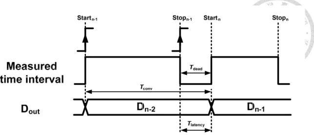
It is apparently that the measurement of a time interval takes time. The time between the start event and output of the measurement result is specified as the conversion time
T
conv and time between the stop events and the output results is called latency Tlatency as shown in Fig 2.3. The time for a TDC to start a new measurement after the end of the previous measurement is called dead time Tdead.Fig. 2.3. Timing figure of the time-to-digital conversion.
2.3 General TDC architecture
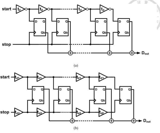
Fig 2.4 (a) shows a conventional delay-line-based digital TDC which is also called
flash TDC. This architecture uses only standard cell of the CMOS process which is suitable for advance CMOS technology. Featuring low cost, low power and high integration level, this architecture gains particular interest. And the resolution of the TDC can be expressed asLSB d
T
t .
(2.3.1)The main drawback of this TDC is that the timing resolution of the TDC is limited to its minimum gate delay which is about tens of picoseconds in 90-nm CMOS.
(a)
(b)
Fig. 2.4. (a) Conventional delay-line-based TDC and (b) Vernier type delay-line-based TDC.
delay-line to the conventional architecture as shown in Fig 2.4 (b) [1]. For the improved TDC, the start and stop are both fed to a series of delay cells and are fed into an arbiter in each stage. The delay td2 is designed to be smaller than the delay td1 so that the stop signal can catch up the start signal along the delay line stages. The output code of the TDC is the summation of the stage output. By adding another delay-line at the stop signal path, the resolution of the conventional delay-line-based TDC can be improved to
LSB d1 d2
T
t
t .
(2.3.2)Theoretically, the resolution of the improved TDC can be design to be any value. The difference of the delay td1 and td2 can be made to be as small as possible. In practice, the resolution of the TDC is limited by the process variation. Mismatch of the delay cells and physical noise of the transistors would limit its overall resolution. Besides, this architecture needs extra hardware for extending input range. For the Vernier delay line, the maximum dynamic range is limited to
DR LSB
T
N T ,
(2.3.3)where N is the number of delay cells in the delay line. Introducing a clock signal with the period equal to the dynamic range of the Vernier delay line TDR and counts the rising edge of the clock, the dynamic range of the TDC can be sufficiently extended.
Calibration circuit is needed to insure that the clock period is equal to the dynamic range of the Vernier delay line TDR [1]. A Vernier ring TDC has been published to overcome the limitation of the input range [2] without the need of calibration.
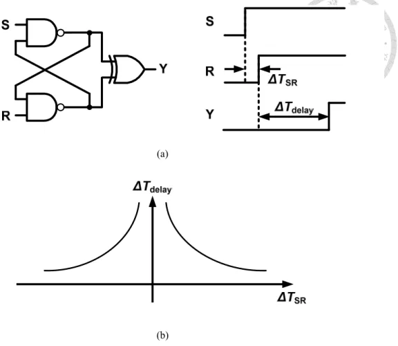
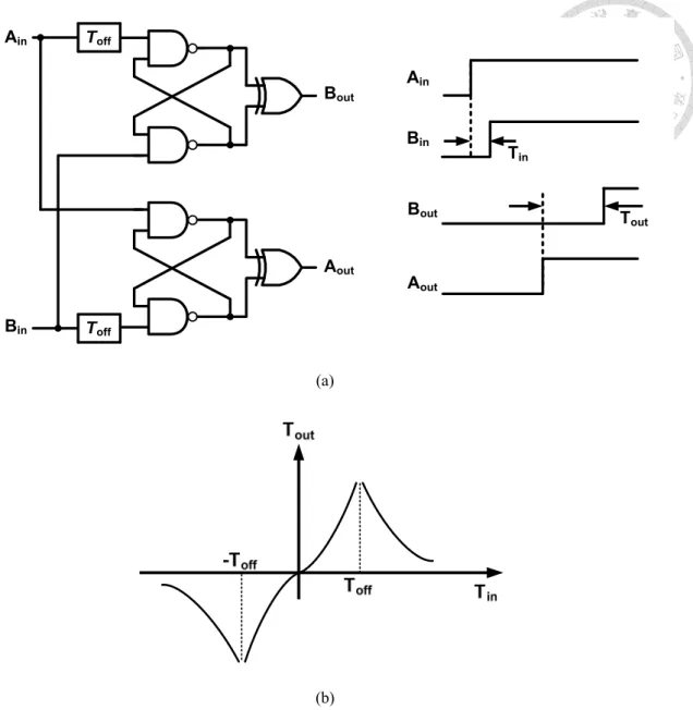
Time amplification TDC achieves high resolution with low area [3]. This TDC employed a two steps conversion to resolve the time interval. The input time interval is first quantized by a coarse TDC to generate the coarse output code and the residual time from the coarse TDC is fed to a time amplifier. The fine TDC then resolves the amplified residual time and produces the fine output code. The key building block of the
TDC is the time amplifier (TA) utilizes the metastability of a SR latch to amplify a time interval. The SR latch exhibits variable delay when nearly coincident input edges are fed to the SR latch as shown in Fig 2.5 (a). Fig 2.5 (b) shows the relationship between the delay time of SR latch and the input time difference. The relationship can be described as [3]
delay TH SR
Δ
T
logV
log
ΔT ,
(2.3.4) where τ and α are constant defined by the physical quantities, and VTH is the threshold voltage of the exclusive OR (XOR). Adding a delay Toff in one of the input path, the transfer curve shown in Fig 2.5 (b) can be shifted for the y-axis. Combining two SR latch with additional delay Toff, the time amplifier can be realized as shown in Fig 2.6.The time amplifier output time Tout is the delay time of the top SR latch minus the delay
(a)
(b)
Fig. 2.5. (a) SR latch followed by an XOR with its timing diagram and (b) the relationship between the delay time of SR latch and the input time difference.
time of the bottom SR latch and can be described as follows
out Δ delay,top Δ delay,bot
T
T
T .
(2.3.5)Substituting (2.3.4) into (2.3.5), the output time can be rearranged as
out log off in log off in
T
T
T
T
T
.
(2.3.6) where Tin is the time difference between the two input edges and is ranging from -Toff toT
off. By adding the time amplifier to realize the two-step TDC, the resolution of the time domain quantizer can be greatly relaxed.Time-to-digital converter based on cyclic time domain successive approximation
Bout
Toff
Toff Ain
Bin
Aout
Ain
Bin
Bout
Aout
Tin
Tout
(a)
(b)
Fig. 2.6. (a)Concept of a TA (b) and input/output transfer curve of a TA
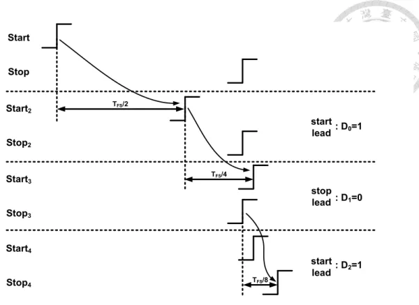
(CTDSA) achieves high resolution with wide dynamic range [4]. The conceptual timing diagram of a 3-bit CTDSA is shown in Fig 2.7. The CTDSA measures the time difference between two signal, start and stop in Fig 2.7. At the beginning of the measurement, the signal start is delayed by a time TFS/2. The delayed signal is shown as
start
2 in Fig 2.7 and the MSB of the TDC is determined to be one since the signal start2leads the signal stop2. The signal start2 would then be delayed by a time TFS/4 and the second bit is generated to be zero because the signal stop3 leads signal start3. Finally, the stop3 is delayed by a time TFS/8 and the LSB is one. Compare to the delay-line based TDC, the successive approximation (SAR) method can effectively reduce the required hardware for wide sensing range due to the use of single delay element with adjustable delay time. The delay cell with adjustable delay time is fulfilled by using cascaded inverter with digital controlled capacitive loading.
Although the TDC with time amplification or successive approximation can achieves high resolution, complicated calibration is needed to calibrate the time amplifier’s gain
Start
Stop
Start2
Stop2
Start3
Stop3
Start4
Stop4
TFS/2
TFS/4
TFS/8
: D0=1
: D1=0 start lead
stop lead
start lead : D2=1
Fig. 2.7. Conceptual timing diagram of a 3-bit CTDSA.
or the delay time of the delay element.
Apart from the TDC mentioned above, several architectures have been published to achieve fine-resolution. A pipeline TDC [5] achieves 300-MHz conversion rate with 1.76-ps resolution and a cyclic TDC [6] achieves 10-MHz conversion with 0.63-ps resolution while consuming 0.82 mW. For those TDCs, sophisticated calibration usually needed to calibrate its non-linearity. A stochastic TDC [7] realized in 14nm FinFET technology has been proposed to achieve 1.17-ps resolution with 100-MHz conversion rate without calibration.
2.4 Delta-sigma TDC
Before this section, the mentioned TDC operations are analogous to the conventional flash, two step, pipeline, SAR ADC. In this section, the TDC analogous to ADC that achieves the noise-shaping property is presented. The effective resolution can be greatly improved as the quantization noise is first-order shaped. Fig 2.8 shows a measured time interval Tin[n] represented by a pulse width and a delay-line-based TDC continuously measures the time. The dot-line shows the continuous quantization of the time interval and the time Tin can be described as follow
Da[n]Da[n-1]
TLSB= [n]Tin
[n]
[n-1] .
(2.4.1) where the Da[n] and Da[n-1] are the accumulated digital outputs, TLSB the timingFig. 2.8. Continuous time measurement of the interval.
resolution of the TDC, ε[n] and ε[n-1] are the quantization errors. Equation (2.4.1) shows that the total quantization error within the time Tin[n] is the difference of two quantization errors from the consecutive delay line sampling. Taking z-transform of (2.4.1) yields
-1 -1
a LSB out LSB in
(1-z )
D
(z)T
D
(z)T
T
(z)
(z) (1-z ), (2.4.2) which shows the quantization noise is first-order shaped. The theoretical rms value of the quantization noise power can be written as-( +1 )
LSB 2
rms
π
12 2 1
L
T L
OSR ,
L (2.4.3)
where the OSR is the oversampling ratio, and L is the order of the noise-shaping function.
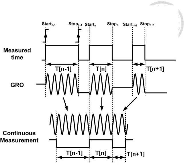
In practice, the measurement of the input time interval is non-continuous as shown in
Fig 2.9. The measurement of a time interval is often initiated by the rising edge of signal
Fig. 2.10. Schematic of GRO and its transient operation.
start and ends at the falling edge of the signal stop and the next measurement will not
start until the next rising edge of signal start.
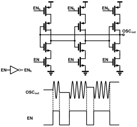
Due to the fact that the measurement is discrete, a TDC with gated-ring oscillator (GRO) [8] is proposed to achieve the noise-shaping property. The simplified schematic of the GRO is shown in Fig 2.10 , consists of three cascaded inverters and three pairs of switches controlled by the signal EN & ENb. The GRO only oscillates when the signal EN is high and hold its phase when EN is low. Feeding the input time to the GRO as shown in Fig 2.11, the conceptual operation principle of GRO-TDC is shown in Fig
2.12. Controlling the by the measured time, the GRO only oscillates during the
measured time interval. The digital output is produced by counting the rising edge of the GRO during the measured time interval. The discrete measurement of the GRO-TDC can be mapped into a continuous measurement of a delay-line-based TDC shown in Fig2.8 which achieves first-order noise shaping of the quantization noise. The output of the
GRO-TDC can be represented as follow
in out
LSB LSB
[n] [n-1]
[n]=
T
[n] .D T T
(2.4.4)
Using GRO to realize the TDC, the GRO-TDC achieves sub-gate delay resolution while occupying low area without calibration. Compare to other TDCs, the GRO-TDC
Fig. 2.11. Architecture of the GRO-TDC.
consumes large power due to the use of a multi-path GRO. Ideally, the phase is preserved completely when the GRO is turn off. However, the charge injection from the switches and the leakage of the transistors cause harmful error to the oscillator phase as shown in Fig 2.13. Multi-path structure reduces the leakage problem at the cost of high power consumption.
Many other TDCs have been published to mitigate the leakage problem. Fig 2.14 shows a conceptual timing diagram of a switched-ring oscillator TDC [9]. The SRO-TDC uses the input time window as the control signal of the ring oscillator. The SRO oscillates at its maximum frequency fmax when the input is high and oscillates at the minimum frequency fmin when the input is low. The phase change of the SRO within
Fig. 2.12. Illustration of noise shaping in the discrete time measurement.
a sampling period can be described as
SRO[n] 2π
D
out[n] Q[n] Q[n+1],
(2.4.5)where the Dout is the digital output of the TDC and
Qthe quantization error. The digital output is the number of oscillator rising edges happened within a clock cycle. And the input Tin is represented asin max min SRO C min
2π
T
[n](f
f )
[n] T f .
(2.4.6) Substituting (2.4.6) into (2.4.5), the TDC output can be obtained asout in max min C min
[n]- [n+1]
[n] [n] ,
2π
Q Q
D T (f f ) T f
(2.4.7)
Fig. 2.13. Leakage induced timing skew error in GRO.
T
inOSC
outT
Cwhich shows the first-order shaped of the quantization noise. Since the ring oscillator is not fully gated, the leakage problem can be reduced. Although the leakage problem can be reduced, the raw resolution TLSB of the SRO-TDC becomes 1/(fmax-fmin). Compare to the GRO-TDC which has a raw resolution of 1/fmax, the SRO-TDC has a reduction in its raw resolution. Thus, the SRO-TDC needs high OSR to achieve high resolution.
Besides, the SRO is always oscillating even if there is no input feeding into the TDC, the power of the TDC therefore increases.
A 1-1-1 MASH TDC is presented to further improve the TDC performance [10]. Similar to a 1-1-1 MASH ADC, a third-order TDC is formed by cascading three first-order TDC. The 1-1-1 MASH TDC works as follow: the measured input time is fed to the first TDC and the first TDC produces the digital output
10
010
110
210
-1610
-1410
-1210
-1010
-810
-6OSR
effective resolution (s)
L=1 L=2 L=3 L=order of noise shaping funtion
Fig. 2.15. Simulation results of the TDC effective resolution.
D
out1. Then, the time domain quantization error of the first TDC is fed to the second TDC and the quantization error of the second TDC is fed to the third TDC. With the help of digital signal processing the combination of the three TDC output achieves third-order noise-shaping. Considering the z-transform of a TDC digital output, each output of the three stages is:-1 out1(z) LSB in(z)+ (z) (z -1)1
D
T
T
(2.4.8)-1 out2(z) LSB 1(z)+ (z) (z -1)2
D
T
(2.4.9)-1 out3(z) LSB 2(z)+ (z) (z -1),3
D
T
(2.4.10)where TLSB is the oscillation period of the oscillator used in the TDC. By combining the three stage outputs in the digital domain, the overall digital output of the 1-1-1 MASH TDC is
-1 -1 2
out(z) out1(z) out2(z) (1-z ) out3(z) (1-z )
D
D
D
D
(2.4.11)-1 3 3
in
LSB LSB
(z) (1-z ) (z)+
T ,
T T
(2.4.12)
where
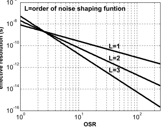
3is the quantization error in the third stage. According to (2.4.3), the rms value of quantization noise power of a third-order TDC is 100 times lower than the first-order TDC if the OSR is chosen to be 20. Due to the large improvement of the quantization noise power in the proposed TDC, the requirement of the oscillation periodT
LSB for a high resolution TDC can be released. To mitigate the leakage problem of the ring oscillator, the ring oscillator in the 1-1-1 MASH TDC uses large capacitance.Simulation has been done for an example TDC with TLSB equals to 16 ns. Fig 2.15 shows the simulated effective resolution of the TDC with different order of noise shaping function. If an OSR of 250 is employed, the third-order TDC can achieve a 0.2-fs resolution which is much lower the physical noise floor of the TDC. It should be
noted here that the oscillator period TLSB of each stage should be the same to completely cancel the quantization error of the first stage and the second stage.
A 1-3 MASH forth-order TDC [11] achieves picosecond resolution with an OSR of 5. The forth-order TDC is capable of achieving high resolution with high signal bandwidth. This TDC is implemented using two stage architectures. The first stage is the conventional first-order GRO-TDC. Consisting of a GRO-TDC and an error-feedback filter, the second stage is implemented as a third-order TDC. The high order TDC enhances the signal bandwidth of the TDC but the resolution of the TDC still suffered from the GRO leakage current and the switching noise from the switches.
Chapter 3
A Noise-Shaping Time-to-Digital Converter with Gated-Free Ring Oscillator
3.1 Introduction
An energy efficient delta-sigma time-to-digital converter (TDC) is presented in this chapter. The proposed delta-sigma TDC achieves high resolution by leveraging oversampling and noise-shaping. Compared with conventional circuit techniques, non-ideal effects associated with switching noise and transistor leakage can be generally prevented due to the use of a gated-free ring oscillator and leakage-suppression switches in the circuit implementation.
The remainder of this chapter is organized as follows. Section 2 describes the architecture of the proposed TDC while the circuit design and experimental results are presented in Section 3 and 4, respectively. Finally, a conclusion is provided in Section 5.
3.2 Proposed delta-sigma TDC
3.2.1 Conventional gated ring oscillator TDC
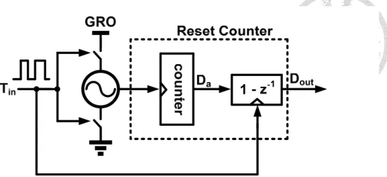
A simplified block diagram of a conventional TDC using gated ring oscillator [8]
and its timing diagram are shown in Fig. 3.1. The measurement of the input time interval is conducted by enabling the ring oscillator and counting the rising edges during this period of time. The ring oscillator oscillates when the input at Tin is high. On the other hand, when Tin goes low, the oscillator preserves the oscillation state by holding
1 - z-1 Dout
Tin
Reset Counter OSC
(a)
(b)
Fig. 3.1. (a)The simplified block diagram and (b) the timing diagram of the GRO-TDC.
the charge at the output node. As illustrated in Fig. 3.1(b), the solid line of OSC indicates the oscillator output waveforms while the dotted line shows the expected waveforms if the ring oscillator is not gated. By preserving the oscillation state, the quantization error is transferred to the next cycle. Consequently, the input can be expressed as
[ ]= [ ] + [ 1] [ ]
in out GRO Q Q
T n D n T
T n
T n
(3.2.1)where the TGRO is the oscillation period of the gated ring oscillator and TQ is the quantization error of the TDC. According to (3.2.1), it is apparent that the quantization noise of the gated ring oscillator TDC is first-order noise shaped. However, special care has to be taken in the ring oscillator design to mitigate its non-ideal effects such as switching noise from gating transistors and leakage of the inverter stages. In order to avoid the error caused by switching noise and leakage, the transistor size and the output capacitance of the inverter stages should be relatively large. As a result, the oscillation frequency of the gated ring oscillator is severely limited, making it less attractive for high-resolution TDC designs.
3.2.2 Proposed delta-sigma TDC
Figure 3.2 shows the proposed TDC and its conceptual timing diagram. Unlike
conventional gated ring oscillator TDC, the proposed circuit does not preserve the state of the ring oscillator and no gating transistors are required. Instead, a NAND gate is added in the ring to control its oscillation as shown in Fig. 3.2(a). As illustrated in Fig.3.2(b), the ring of the proposed TDC starts oscillating at the rising edge of the start
signal. At the rising edge of stop, the time register generates a time interval Treg, which(a)
(b)
Fig. 3.2. (a) The architecture of the proposed TDC and (b) its conceptual timing diagram.
is given by TFS minus the time-domain quantization error from the previous cycle, that is TFS-TQ[n-1]. TFS represents the full scale discharge time of the capacitor. After the falling edge of Treg, the control signal stopint is triggered and fed to the multiplexers to stop the oscillation. It is noted that the time interval from the falling edge of Treg to the second rising edge of VGFRO is the quantization error TQ[n]. Therefore, this error is memorized in the time register for the next cycle and the digital output is obtained by counting the rising edge at the output of the ring oscillator. In order to have a gated-free operation, the proposed TDC allows the oscillator to start at the same state rather than preserve the state of the ring oscillator. By shifting the time-domain quantization error as illustrated in Fig. 3.2(b), the input time interval of the TDC is given by
[ ] ( [ ] 1) [ 1] [ ]
in out GFRO FS Q Q
T n
D n
T
T
T n
T n
(3.2.2) where TGFRO is the period at the output of the gated-free ring oscillator. The TFS is a constant time interval due to the time register. With z-transform of (3.1.2), the digital code at the output can be expressed as( ) (1 1) ( )
[ ] in FS Q 1,
out
GFRO
T z T z T z
D z
T
(3.2.3)
showing a first-order noise shaping property for the TDC. The reason for the plus one at the digital output is that the gated-free ring oscillator is always stopped at the first rising edge after the stop signal is rising.
3.3 Circuit implementation 3.3.1 Time Register
To realize the operation of the proposed TDC, a time register is utilized in the design, consisting of switches SWn and SWp, two capacitors, a resistor and logic gates as shown in Figure 3.3. Unlike voltage-mode ADC circuits, the time-domain quantization error is difficult to be memorized and transferred. Therefore, a time-to-voltage operation is adopted to store the time-domain information [6] and the two capacitors operating alternatively in consecutive cycles are used for this purpose. Figure 3.4 shows the transient operation of the time register by illustrating the nodal voltage V1 and V2. At the end of the measured time interval, in other words, the rising edge of the signal stop, the first capacitor starts to discharge. The full scale discharge time of the capacitor is TFS
defined by the RC time constant of the circuits. For instance, the TFS is simply 0.693R0
C
0 if the inverter threshold is VDD/2. Since the first capacitor has been discharged for a time interval of TQ[n-1] during the previous cycle, the remainingFig. 3.3. Block diagram of the time register.
discharge time of first capacitor would be TFS-TQ[n-1] in the nth cycle, as depicted in Fig.
3.4. As the voltage of the first capacitor drops to the switching threshold of the inverter,
the time register starts discharging the second capacitor until the second rising edge of the ring oscillator. Consequently, the time-domain quantization error of current cycleT
Q[n] is memorized by the second capacitor while the first capacitor is reset to VDD. The operations of the two capacitors exchange in the next cycle to generate the required Tregfor the TDC. It is noted that TFS should be larger than 2TGFRO to ensure the time register work properly. The mismatch of the two capacitors is neglected here because the noise caused by the mismatch of the two capacitors would be filtered out by the decimation filter for filtering out high frequency quantization noise.
3.3.2 Leakage Suppression Switches
Although the leakage problem is alleviated for the ring oscillator due to the absence of the gating transistors, it may still lead to undesirable errors for the time register. Due to the low voltage operation in the proposed design, the size of switches should be large
Fig. 3.4. Transient operation of the time register.
enough to minimize the time to charge the capacitor otherwise the conversion speed and the input range is limited. But the leakage problem becomes exaggerated as the large size switches is used. Therefore, a leakage-suppression technique [12] is adopted to realize the switches SWp and SWn.
Figure 3.5 shows the circuit schematic of the
switches controlled by S0-S3. When the leakage suppression switches are off, negative voltages Vsg and Vgs are provided for M1 and M2, respectively. The reversed source-gate voltage results in a significant reduction of the leakage current. Compared with the single transistor switches, the leakage suppression technique consumes more power and occupies more area. Since the ring oscillator often operates at a frequency much higher than the input rate, using the leakage-suppression switches in the gated ring oscillator is impractical due to excessive power overhead. The cascaded structure of the leakage suppressions limits the oscillator frequency. On the other hand, as these switches in the proposed TDC only toggles once in each clock cycle, it is well suited for the implementation of the time register3.3.3 Gated-free ring oscillator
One of the key building blocks of the proposed TDC is the gated-free ring oscillator.
The schematic of the gated-free ring oscillator is shown in Fig 3.6. To ensure the proposed TDC work properly, the frequency variation of the gated-free ring oscillator
Fig. 3.5. Schematics of the leakage suppression switches
should be considered. In order to realize a high resolution TDC, it is better to minimize the period of the ring oscillator (TGFRO). Due to the limited speed of the counter, the period of gated-free ring oscillator is designed to be 6 ns. The lengths of the transistors are designed to be slightly larger than the minimum size of the device to mitigate the process variation. From one hundred times Monte-Carlo (MC) simulations, the standard deviation of the oscillation period is 270 ps. Because of the large passive device size used in the time register, the standard deviation of full scale discharge time (TFS) of the time register is only 8 ps which is tolerable in the proposed design.
3.3.4 Noise analysis
Considering the quantization noise power, the SNR of the proposed TDC can be calculated as [10]
signal q.rms
10log
P
SNR P
(3.3.1)
1=10 log 6(2 +1) 10 20 ( + ) log(OSR) 20 log(2 -1), 2
L L L
N (3.3.2)
M1 M2
M3 M4
M5
M6
M7
M8
Fig. 3.6. Schematic of the gated-free ring oscillator
where L is the order of the noise function, OSR oversampling ratio, and N the bits of the quantizer. In the proposed design, the L is set to be 1, the OSR is set to be 10, and a 7 bits quantizer is used. The theoretical SNR of the proposed TDC is calculated to be 74.6 dB, that is, an ENOB of 12.1 bits. However, the resolution of a practical TDC is limited by the jitter from the ring oscillator, the jitter from the time register, and the charge injection and charge redistribution from the switches. Those circuit non-idealities severely degrade the TDC performance especially in the low voltage design. Among those non-idealities, the jitter from the ring oscillator dominates the TDC performance.
The charge redistribution and the charge injection can be neglected here because of the large capacitor used in the time register and the thermal noise from the switches and the resistor only depend on the size of the capacitor. Large device size is used to implement the inverters to suppress the flicker noise. In order to achieve a micro-power design, the transistors of the ring oscillator can’t be excessively large and so as the parasitic capacitance. The size of the transistors used in the ring oscillator is just slightly larger
102 103 104 105
-100 -80 -60 -40 -20 0
frequency [Hz]
Output spectrum [dB]
Fig. 3.7. Simulated output spectrum of the TDC.
than the minimum size to mitigate the process variation. Assuming that the jitter of the ring oscillator is caused by white noise, the SNR of the TDC can be derived as
2 signal
jitter
10log 22 T SNR
OSR
(3.3.3)
where Tsignal is the full scale of the input time, and the σjitter is the rms jitter of the ring oscillator. The transistor level simulation shows that the rms jitter of the ring oscillator is about 29 ps. Thus, for an OSR of 10, the theoretical SNRof the TDC is 94.6 dB. Fig
3.7 shows the simulated output spectrum of the TDC with the presence of ring oscillator
jitter. The integrated noise within 50-kHz bandwidth is 67 ps.3.4 Experimental Results
3.4.1 Measurement at 0.3-V supply voltage
The TDC is fabricated by using a 90-mm CMOS process. Figure 3.8 shows the photomicrograph of the prototype circuit with a chip area of 0.0082 mm2. Operated at a full scale input of 700 ns, the core circuit consumes a total power of 1.5 W from a 0.3-V supply.
The static characteristics of the TDC were first investigated by applying a ramp input.
For a 1-MHz input signal and a 0.999998-MHz clock, the transfer curve is obtained as shown in Fig. 3.9(a) after filtering the output with a 50-kHz digital low-pass filter.
Figure 3.9(b) illustrates the integral nonlinearity (INL), which is extracted from the
linear fit of the transfer curve, indicating a maximum INL value of +1.83/-1.84 LSB.With a 40-ps peak-to-peak sinusoidal input at 885 Hz, the power spectrum density (PSD) of the TDC output is characterize. The experimental results are shown in Fig. 3.10, where the first-order noise shaping is clearly observed. Note that, since it is difficult to generate a highly linear time-domain sinusoidal input, a small input signal generated by
Fig. 3.8. Chip photo.
an on-chip delay line is used to evaluate the TDC noise performance as shown in Fig.
3.11. Adding varactors on the delay path, the delay of the stop signal is controlled by
applying sinusoidal wave to the varactors. Using this method, the input jitter can be minimized since the jitter from the instrument can be removed. The measured integrated noise of the proposed TDC is 113 ps within a bandwidth of 50 kHz. In contrast to the simulation results, the low frequency noise from the flicker noise in the ring oscillator and the supply noise dominates the overall resolution.0 100 200 300 400 500 600 700 0
2048 4096 6144 8192
Input time [ns]
Output code
(a)
0 1024 2048 3072 4096 5120 6144 7168 8192 -4
-2 0 2 4
Output code
INL [LSB]
(b)
Fig. 3.9 Measured (a) DC transfer curve and (b) corresponding INL at 0.3-V supply.
In addition, single-shot-precision (SSP) test was performed by applying a constant input to the TDC. In order to minimize the input clock jitter, the time difference of the two input clocks is generated by the delay of a connector cable. The experimental results of the SSP are shown in Fig. 3.12. With an input of 3.1 ns, the RMS noise of the filtered output code is 75.6 ps. It is noted that the discrepancy between the RMS noise
102 103 104 105
-100 -80 -60 -40 -20 0
Frequency [Hz]
Output Spectrum [dB]
Fig. 3.10 Measured PSD for a 885-Hz input at 0.3-V supply.
Fig. 3.11 Schematic of input-delay lines.
from the SSP test and the integrated noise from the dynamics test is due to the different measurement setup.
34 35 36 37 38 39
0 1 2 3 4 5 x 10
5Output Code
Hi t Co un t
Fig. 3.12 Measured single-shot precision of the prototype TDC at 0.3-V supply.
3.4.2 Measurement at 0.6-V supply voltage
The power consumption of the TDC at 0.6-V supply voltage is 56 W with a full-scale input range of 70 ns. By applying a 10-MHz and a 9.9999-MHz clock to the TDC, the measured DC transfer curve is obtained after filtering the output code with a 250-kHz digital filter as shown in Fig 3.13. The INL of the proposed TDC is obtained from the deviation of the transfer curve from the best fit line as shown in Fig 3.13 (b) and the worst case INL is +7.1/-6.3 LSB.
Fig 3.14 shows the output spectrum for a 10-ps peak-to-peak, 22.6-kHz time-domain
0 10 20 30 40 50 60 70
0 2048 4096 6144 8192
input time [ns]
Output code
(a)
0 1024 2048 3072 4096 5120 6144 7168 8192 -10
-5 0 5 10
INL [LSB]
Output code (b)
Fig. 3.13 Measured (a) DC transfer curve and (b) corresponding INL at 0.6V-supply.
sine-wave input. The integrated noise within 250 kHz is 15.7 ps. The results of SSP test is shown in Fig 3.15 with an approximately constant input of 197 ps and the RMS noise of the filtered output code is 3.2 ps.
The GFRO is the major source of the thermal/flicker noise within the TDC. The device noise of the GFRO shows as the phase noise of the GFRO and the phase noise exhibits 1/f2 and 1/f3 profiles in the thermal and flicker noise limited regions. Because of the reset counter, the output of the TDC has a flat spectrum in the thermal noise limited region. In the flicker noise limited region, the spectrum exhibits -10dB/decade slope.
To best characterize the TDC performance, the calculation of the ENOB considers both the linearity and the noise performance of the TDC [11]. The SNDR of the TDC is defined as
TDC 10 S
D N
10log (
P
),SNDR
P P
(3.4.1)
where Ps, PD and PN are time-domain signal power, distortion power, and noise power
103 104 105 106
-120 -100 -80 -60 -40 -20 0
frequency [Hz]
Output spectrum [dB]
Fig. 3.14 Measured PSD for a 22.6-kHz input at 0.6-V supply..
to the static test and the SSP test as
2 range
s=1 1( )
P
2 2 T
(3.4.2)(6.02 lin+1.76) 10
D S 10- N
P
P
(3.4.3)2
N SSP
P
.
(3.4.4)where Nlin is defined as
N
lin Bits log (INL+1). 2Then the ENOB of the TDC can be
21 22 23 24 25
0 1 2 3 4 5 6 7 8 9x 10⁵
Output code
Counts
σ
ssp=3.2 ps
Fig. 3.15 Measured single-shot precision of the prototype TDC at 0.6-V supply.
Table 3-1 TDCPERFORMANCE AND COMPARISON WITH STATE-OF-THE-ART.
Delta Sigma TDC
[8] [9] [10] [11] This Work Order 1st 1st 3rd 4th 1st Process(nm) 130 90 130 65 90
Supply(V) 1.5 1 1.2 1 0.3 0.6 Area(mm2) 0.04 0.02 0.11 0.03 0.0082
fBW(MHz) 1 1 0.1 15 0.05 0.25 fs(MS/s) 50 500 50 150 1 10
Trange(ns) 12.29 12.5 20 5.4 700 70
resolution (ps) 0.28* 1.09* 5.6 2.64* 391* 54*
Power(uW) 21000 2000 1700 3520 1.5 56 FoM(pJ/conv.) - 0.86 - 0.19 0.0076 0.112/0.018**
*Estimated resolution ( Tint,2rms12).
**The FoM is calculated without distortion power.
obtained as
TDC
1.76 6.02
ENOB
SNDR
(3.4.5)For comparison, a widely used figure of merit (FoM) is given as [4]
2 2
TDC ENOB
Power
FoM
BW
(3.4.6)
The performance of TDC is tabulated in Table 3-1. With 1.5-W power, 10.9 ENOB and 50-kHz bandwidth, the proposed circuit demonstrates the lowest FoM among the state-of-the-art TDC designs. Table 3-1 also shows the TDC performance while operating at 0.6-V supply. The TDC achieves an ENOD of 10 bits at 250-kHz signal bandwidth and draws a total power of 56 W from 0.6-V supply. As the non-ideal effects associated with the switching noise and transistor leakage are alleviated in the proposed circuit technique, the trade-off between oscillation frequency and timing skew error is therefore relaxed such that the performance of the TDC can be optimized.
3.5 Conclusion
This chapter presents a highly-digital TDC using a gated-free ring oscillator.
Fabricated in a 90-nm CMOS process, the circuit achieves an ENOB of 10.9 bits with 50 kHz bandwidth while consuming 5 A from a power supply of 0.3V. Operating at 0.6-V supply voltage, the proposed TDC achieves 10 bits ENOB with 250 kHz bandwidth and draws 93 A from a power supply of 0.6V. It is well suited for low-cost and low-power time-to-digital conversions with sufficiently high resolution.
Chapter 4
Time-Mode Capacitive Sensor Interface with Second-Order
Time-to-Digital Converter
4.1 Introduction
Capacitive sensors present high power consumption and low conversion speed due to the use of analog-to-digital converter (ADC) and the capacitance-to-voltage circuits [15][16]. Additionally, the reduction of the supply voltage in nanometer technologies leads to the scaling difficulties in mixed-signal data conversion based on a signal representation in voltage-domain. In order to overcome the limitations that the ADC-based interface circuits present for capacitive sensor, several time-mode capacitive sensor interfaces has been published [17][18][19]. To achieve high resolution with energy efficiency, second-order modulator has been implemented in the proposed design. In this chapter, capacitance-to-digital (CDC) converter with capacitance-to-time converter and a proposed second-order time-to-digital (TDC) converter is presented. Instead of using the MASH architecture, the proposed TDC composed of only one oscillator and the Gated-delay buffers. Based on the concept of time register, the gated-delay buffers memorize the quantization error of the TDC and
feedback to the input of the TDC to fulfill the second-order modulator. Due to the highly digital architecture and the signal representation in the time-domain, the TDC allows reducing the required supply voltage and the power consumption with sufficient resolution.
The rest of this chapter is organized as follows. Section 4.2 illustrates the architecture of the proposed second-order capacitance-to-digital converter, while detail circuit implementation and experimental results are presented in Section 4.3 and 4.4, respectively. Finally, a conclusion is provided in Section 4.5.
4.2 Proposed capacitance-to-digital converter
The proposed capacitance-to-digital converter consists of a capacitance-to-time converter and a second-order TDC as shown in Fig 4.1. To better understand the operation principle of proposed second-order TDC, a 1-1 MASH TDC [13] will be illustrated before the proposed TDC.
4.2.1 1-1 MASH TDC
To enhance the TDC performance, high order TDC implemented using MASH structure has been demonstrated in [10][11]. In order to give an insight to the proposed
Capacitance-to-Time TDC D
out Fig. 4.1. Time-mode capacitance-to-digital converter.Fig. 4.2. Simplified block diagram of the 1-1 MASH TDC.