Investigation of the interlayer characteristics of Ta
2O
5thin films deposited
on bare, N
2O, and NH
3plasma nitridated Si substrates
Yi-Sheng Lai, Kuan-Jen Chen, and J. S. Chena)Department of Materials Science and Engineering, National Cheng Kung University, Tainan, Taiwan 共Received 3 December 2001; accepted for publication 1 March 2002兲
Low-temperature N2O and NH3 plasma nitridations on Si surfaces are conducted to prevent the thermodynamic instability at the Ta2O5/Si interface. The surface and interface of the Ta2O5/Si systems, without or with nitridation, were examined by x-ray photoelectron spectroscopy 共XPS兲, atomic force microscopy, transmission electron microscopy, and secondary ion mass spectrometry. Capacitance–voltage (C – V) measurements were carried out to investigate the electric/defect characteristics of the Ta2O5/Si systems. For the non-nitrided Si substrate XPS detects no surface
oxide formed prior to Ta2O5 deposition. In contrast, NH3 plasma nitridation forms a nitrogen-rich
SiOxNy layer, while N2O plasma nitridation produces an oxygen-rich SiOxNy layer on Si. C – V
measurement reveals high densities of fixed charges, trapping sites, and interface states in the Ta2O5/non-nitrided Si sample, indicative that a defective interlayer was formed during Ta2O5
deposition. Ta2O5on both nitrided systems exhibits a reduced amount of fixed charges and trapping
sites. Nevertheless, NH3 plasma nitridation is not as effective as N2O plasma nitridation in
diminishing the density of interface states. The different electric/defect characters between the NH3
and N2O nitrided systems are attributed to the further oxidation of the nitrogen-rich SiOxNylayer
produced by NH3 plasma nitridation, which induces defects at the dielectric/Si interface.
Effectiveness of the nitridation process, therefore, depends on the stability of the nitrided layer during deposition of Ta2O5. © 2002 American Institute of Physics. 关DOI: 10.1063/1.1471926兴
I. INTRODUCTION
As the feature size of ultralarge scale integration devices shrinks, thinner gate oxides are necessary to achieve better channel potential control, higher drive current, and lower threshold voltage of metal–oxide–semiconductor field-effect transistors 共MOSFETs兲. The conventional SiO2 gate
dielec-tric has reached its limits due to the high direct tunneling current. High dielectric constant k materials such as Ta2O5, 1–3 TiO2, 4 ZrO2, 5 HfO2, 6 Al2O3, 7 and BaxSr1⫺xTiO3, 8
are thereby being considered to replace the SiO2. Of these, tantalum pentoxide (Ta2O5), which has been
widely investigated as a thin film capacitor, is a promising candidate for gate dielectric application.
The interfacial characteristics between the gate dielectric and Si are considered to be the most challenging issue for the performance of MOSFETs. Due to the lattice mismatch be-tween high k materials and the Si substrate, an incoherent interface will be developed. This incoherent interface will induce defects or strains that will degrade the electrical per-formance considerably, such as high interface state density, high leakage current, and low breakdown strength. Based on thermodynamics, the Si substrate would reduce the Ta2O5
film and form an interfacial layer, which is considered to be a Si–oxide (SiOx)9layer or a Si–Ta–O layer.10,11Growth of
the interlayer will increase the teq 共equivalent SiO2
thick-ness兲 of the MOS structure. Consequently, an additional bar-rier layer should be added to prevent the reaction. Nitridation
of the Si substrate before Ta2O5deposition is widely used to
prevent the growth of an interfacial layer during Ta2O5
depo-sition and postannealing. Techniques of nitridation include rapid thermal annealing 共RTA兲,12 jet vapor deposition,13and remote plasma chemical vapor deposition 共RPCVD兲.14 The nitridation process usually generates a layer containing Si, O, and N, referred as the ‘‘SiOxNy’’ layer. However, most of the
studies reported in the literature concern the effect of nitri-dation on the teqand leakage characters of Ta2O5.1–3,11The
material characteristics of the SiOxNy layer, both as formed
and after Ta2O5 deposition, have not been thoroughly
inves-tigated. In this work, we have modified the Ta2O5/Si
inter-face by conducting a low-temperature N2O or NH3 plasma
treatment on Si at 450 °C. The process temperature, 450 °C, is much lower than the nitridation temperatures reported in the literature 共T⬎800 °C for conventional furnace or RTA treatments兲.15 Chemical bonding states and microstructures of the Si surfaces, with or without plasma nitridation, are examined before the Ta2O5 deposition. After depositing Ta2O5, the Ta2O5/Si cross sections are analyzed, and defect states at the Ta2O5– Si interfaces are extracted from capacitance–voltage (C – V) measurements on the Al–Ta2O5– Si MOS structures. The correlations between the
formation of defects and the material characteristics of samples under various nitridation treatments are discussed below.
II. EXPERIMENT
Bare n-type共100兲 silicon wafers 共resistivity: 1–10 ⍀ cm兲 were used as substrates. The Si surface was cleaned by a a兲Author to whom correspondence should be addressed; electronic mail:
6428
关Ta(OC2H5)5兴 with oxygen, without exposing the sample to
the air. The total chamber pressure was controlled at 1 Torr and temperature was set at 450 °C during Ta2O5 deposition.
The thickness of the resulting Ta2O5 films was in the
range of 25–35 nm, as determined by the ellipsometer. Chemical bonding states of Ta2O5 films and nitrided Si
sur-faces were examined by VG ESCA-210 x-ray photoelectron spectroscopy共XPS兲 equipped with a monochromatic Mg K␣ source. Due to charge accumulation on the insulator surface, the spectra were corrected by shifting the peak of the Si 2 p3/2
to 99.0 eV. The surface roughness and morphology were ex-amined using Digital Instruments Nano-Scope III atomic force microscopy共AFM兲. High-resolution transmission elec-tron microscopy关共TEM兲, Philips TECNAI F20兴 was used to study the cross-sectional microstructure of the samples. Sec-ondary ion mass spectrometry 关共SIMS兲, Cameca IMS-4f兴 analysis was carried out to measure the depth profiles of relevant elements. O2⫹ ions were used as the primary ion beam for SIMS depth profiling. To obtain the electrical char-acteristics of Ta2O5 films, Al/Ta2O5/Si MOS capacitors were fabricated. The top electrodes were circular dots of 130
m diameter. A computer-controlled HP 4284 LCR meter was used for C – V measurements at a frequency of 100 kHz with an ac small signal of 25 mV.
III. RESULTS
A. Characteristics of Si surfaces with or without plasma nitridation
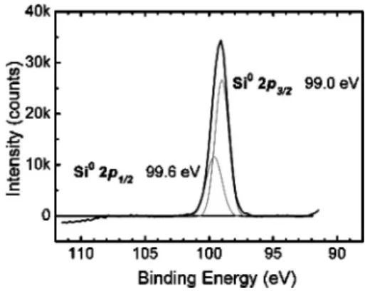
Figure 1共a兲 shows the XPS spectra of Si 2p core levels on the bare Si surface immediately after RCA cleaning and HF dip. The Si0 signal represents the Si bonding in diamond structure where one Si atom bonds to the four nearest Si neighbors. The background from the inelastic electron scat-tering is removed before the spectrum is deconvoluted. The spin–orbit splitting of 0.612 eV16and the area ratio of 1:217 between the Si 2 p1/2, 2 p3/2 were used for fitting the
spec-trum with the Si 2 p1/2and 2 p3/2 peaks. The positions of the decomposed 2 p3/2 and 2 p1/2 peaks were 99.0 and 99.6 eV, respectively.
To investigate the bonding configuration of the native-grown SiOxlayer, we exposed the cleaned Si surface to air at
room temperature for 4 h. The XPS spectrum of Si 2 p core levels is shown in Fig. 1共b兲. The deconvoluted peaks include the Si02 p1/2, 2 p3/2signals emanated from the Si substrates,
and the Si⫹ (Si–Si3O), Si2⫹ (Si–Si2O2), Si3⫹ (Si–SiO3),
Si4⫹(Si–O4) signals. The symbol of ‘‘A-BxCy’’ represents a
bonding structure of one A atom bonded with x B atoms and
y C atoms. Si4⫹ signal denotes the formation of stoichio-metric SiO2 on the surface, while Si⫹, Si2⫹, and Si3⫹ are
intermediate states. The energy shift of the three intermediate states relative to the Si0 peak is referenced from Himpsel
et al.18 The splitting between the Si0 and Si4⫹ signal is 3.8 eV for native-grown SiOx on Si.
In order to clarify the Si surface state before Ta2O5
deposition, we put a cleaned wafer into the CVD chamber and performed a thermal cycle similar to the process before Ta2O5 deposition, whereby the substrate temperature was
raised from room temperature to 450 °C. After being un-loaded, the sample was immediately examined ex situ by using XPS. The XPS spectrum of Si 2 p core levels on the Si surface is shown in Fig. 2. The absence of the Si4⫹ peak suggests that no native oxide had grown on the Si surface before Ta2O5 deposition.
FIG. 1. XPS spectra of Si 2 p core levels on the:共a兲 Si 共100兲 surface after RCA clean and HF dip and共b兲 cleaned Si 共100兲 surface after being exposed to air for 4 h.
FIG. 2. XPS spectra of Si 2 p core levels on the RCA cleaned Si surfaces after ramping to 450 °C and cooling down in the CVD chamber.
As for the nitrided samples, the XPS spectra of N 1s core levels obtained from the Si surfaces experiencing N2O or NH3 plasma nitridation process are shown in Figs. 3共a兲
and 3共b兲. Figure 3共a兲 suggests that the N 1s core levels of the N2O plasma nitrided Si surface is composed of three bonding
configurations. The binding energies are ⬃397.8 eV for N–Si3 structure,19,20⬃398.6 eV for N–Si2,19,20and⬃401.0
eV for N–Si2O,21,22 respectively. However, the integrated
area for the N–Si2O peak is quite small. On the other hand,
the N 1s spectrum of the NH3 plasma nitrided Si surface
关Fig. 3共b兲兴 is composed of two components, which are N–Si3
and N–Si2 structures. The XPS intensity 共integrated area兲
ratio of the N 1s peak to the sum of the N 1s peak and O 1s peak关IN2/(IN2⫹IO2)兴 is 0.65 for the NH3plasma nitridation
sample and 0.08 from the N2O plasma nitridation sample,
respectively. Therefore, even though the nitrogen content in SiOxNy is very different, the N atoms tend to bond with
silicon atoms rather than oxygen atoms for either N2O or
NH3 nitridation.
Figure 4 shows the XPS spectra of Si 2 p core levels on the Si surfaces after plasma N2O and NH3 nitridation. Be-cause the oxygen content is quite high in the SiOxNy layer produced by plasma N2O nitridation, we have deconvoluted the peaks in a configuration similar to that of the native SiOx/Si system 关Fig. 4共a兲兴. The splitting of the energy
be-tween Si0 and Si4⫹ peaks is 4.4 eV in Fig. 4共a兲, which is larger than that in Fig. 1共b兲. This change of the Si0, Si4⫹ energy splitting is most likely due to the different thicknesses of SiO2.23On the other hand, the Si 2 p XPS spectrum of the
plasma NH3nitrided surface关Fig. 4共b兲兴 is difficult to
decon-volute due to the complex bonding environment for Si at-oms. Accordingly, we have assigned the Si0, intermediate state 共Si1⫹, Si2⫹, and Si3⫹兲, and Si4⫹ peaks in Fig. 4共b兲.
The Si4⫹ peak may be associated with Si–O4 共for Si in
SiO2兲 and Si–N4 共for Si in Si3N4兲 bondings. It is thus
de-noted as Si–OxN4⫺x, x⫽0 – 4.
From the spectrum of the Si 2 p core levels, we can cal-culate the thickness of the over layer by the following equation:18
dSiO2⫽SiO2sin␣ln
冋
共I4⫹/I0兲
共I⬁/I0兲 ⫹1
册
, 共1兲where␣is the photoelectron takeoff angle共90° in our work兲, and SiO2 is the photoelectron mean-free path in the SiO2
film experimentally determined to be 21 Å24for the Mg K␣ line. I4⫹and I0are the integrated photoelectron intensities of the Si4⫹ peak from SiO2 and the Si0 peak from bulk Si,
respectively. (I⬁/I0) is the intensity ratio of the Si4⫹ peak from an infinitely thick SiO2 to the Si0 peak of a bare Si
substrate, which is determined experimentally to be 0.50 for Mg K␣ radiation of our XPS system. We can estimate the SiOxNy 共mostly SiO2兲 layer formed after N2O plasma
nitri-dation to be about 22 Å. In contrast, the thickness of the SiOxNy layer formed by NH3 nitridation is difficult to esti-mate because the parameters 共 and I⬁/I0兲 for SiO
xNy are
not available. However, the Si XPS spectrum indicates that Si atoms in this layer are mostly in the Si4⫹ (Si–OxN4⫺x,x⫽0 – 4) state 关Fig. 4共b兲兴. Therefore, by
as-suming that the parameters for the SiOxNylayer are similar
to that for the SiO2 layer, we can roughly estimate the
thick-ness of the SiOxNy layer formed by NH3 plasma nitridation
from the intensity ratio (I4⫹/I0) in Fig. 4共b兲. The estimated thickness is approximately 11 Å.
As a result, NH3 and N2O plasma nitridation processes
both produce an SiOxNy layer. However, the SiOxNy layer
formed by N2O nitridation is rich in oxygen, whereas the
FIG. 3. XPS spectra of N 1s core levels on the Si surfaces after:共a兲 N2O and共b兲 NH3plasma nitridation. Peaks at 397.8, 398.6, and 401.0 eV repre-sent binding structures of N–Si3, N–Si2, and N–Si2O, respectively.
FIG. 4. XPS spectra of Si 2 p core levels on the Si surfaces after共a兲 N2O and共b兲 NH3plasma nitridation.
SiOxNy layer formed by NH3 nitridation is rich in nitrogen.
This is reasonable because N2O is a strong oxidizing agent
and easily releases oxygen to form SiO2 on Si. In
compari-son, plasma N2O nitridation produces a thicker SiOxNylayer
than plasma NH3 nitridation for the same time共10 min兲 at the same temperature 共450 °C兲. The greater thickness of SiOxNyproduced by N2O nitridation shall also be attributed to the high oxidizing strength of N2O. Nitrogen atoms in both SiOxNylayers, however, are mostly bonded to Si atoms rather than to oxygen atoms. In addition, studies in the lit-erature have reported that N atoms in the N2O nitrided layer
are mostly concentrated at the interface near the Si substrate.19–21,25–27 Accordingly, the N atoms in the N2O
plasma produced SiOxNy layer are likely to pile up at the
SiOxNy/Si interface.
The morphological change after plasma nitridation was
examined using AFM and Fig. 5 shows the plasma N2O and
NH3 nitrided Si surface. The root-mean-square values of the
surface roughness Rrmsare 3.55 and 3.59 Å, respectively. In
comparison, the roughness of the RCA cleaned bare Si sur-face (Rrms⫽3.69 Å) is a little higher than that of the plasma
nitrided surface. It is clear that plasma treatment on Si will not degrade the surface morphology. Therefore, the dielectric/Si interface morphology should not be a factor for the consequent differences in the electrical properties of the three systems.
B. Ta2O5 films deposited on non-nitrided and nitrided
Si substrates
After plasma nitridation, Ta2O5 films were deposited in
situ on N2O or NH3 nitrided Si substrates. As a control
sys-tem, Ta2O5 films were also deposited on non-nitrided Si.
From cross-sectional TEM examination, the physical thick-ness of the interfacial layers in Ta2O5/Si, Ta2O5/N2O
plasma nitrided Si, and Ta2O5/NH3plasma nitrided Si
struc-tures are all about 22⫾2 Å. Figure 6 shows the HRTEM micrograph on the cross section of the Ta2O5/NH3 plasma
nitrided Si sample, indicating that the interlayer has a uni-form amorphous structure, and the other two samples exhibit similar characters. Because XPS measurement shows that the substrate without plasma nitridation has almost no oxide on it 共Fig. 2兲, the whole interlayer in the Ta2O5/non-nitrided Si
sample is grown during Ta2O5deposition. On the other hand,
the thicknesses of SiOxNy layers formed by NH3 and N2O
nitridation are estimated to be 11 and 22 Å, respectively. Therefore, the interlayer of the Ta2O5/NH3 nitrided Si also
grows thicker during Ta2O5 deposition, whereas that of
Ta2O5/N2O nitrided Si does not. The various degrees of in-terlayer growth and its effect on the electrical properties of Ta2O5 MOS capacitors are discussed later.
SIMS depth profiles of as-deposited Ta2O5films on N2O and NH3 plasma nitrided Si surface are shown in Figs. 7共a兲 and 7共b兲, respectively. The N content of NH3plasma
nitrida-tion sample is significantly higher than that of the N2O
plasma nitridation sample. Therefore, the high nitrogen con-tent in the SiOxNylayer formed by NH3plasma nitridation is
still preserved after Ta2O5 deposition.
Figure 8 shows the C – V curves of the as-deposited Ta2O5/Si, Ta2O5/N2O nitrided Si, and Ta2O5/NH3 nitrided
Si samples. The relative dielectric constants k of the as-deposited Ta2O5/Si, Ta2O5/N2O nitrided Si, and
FIG. 5. AFM images of: 共a兲 RCA cleaning and HF dip, 共b兲 plasma N2O nitrided Si, and共c兲 plasma NH3nitrided Si substrates.
SiOxNylayer is nitrided by NH3plasma. Thickness of the SiOxNylayer is
Ta2O5/NH3 nitrided Si samples are 12.3, 15.7, and 15.0, respectively. The k values of Ta2O5 films on the nitrided Si are higher than that on bare Si, revealing that the interfacial layer formed by depositing Ta2O5on bare Si exhibits a lower
k value than the plasma nitrided SiOxNy layer.
The flatband voltage Vfbextracted from the C – V curve
共swept from ⫺5 to ⫹5 V兲 of the as-deposited Ta2O5/Si is
⫺1.58 V. This Vfb value has higher negative charges than
that of the conventional SiO2/Si, which is indicative of more
positive fixed charges Qf presented in the dielectrics. On the
other hand, when Ta2O5 films were deposited on plasma
N2O nitrided Si and NH3 nitrided Si, the Vfb values were
⫺0.46 and ⫺0.40 V, suggesting that the positive fixed charges are significantly reduced on the plasma nitrided in-terface.
A forward-and-reversed voltage sweep was performed to study the stability of the dielectrics from inversion to accu-mulation and vice versa. The curves were swept from nega-tive bias 共⫺5 V兲 to positive bias 共⫹5 V兲 and then immedi-ately returned back to the starting point 共⫺5 V兲. Figure 8 indicates a clockwise hysteresis behavior of the C – V curve is observed, which is caused by the trapping of negative charges in the oxide defect states when the MOS capacitor is stressed.28,29These defect states are so-called ‘‘slow trapping
sites.’’30,31The following equation can be used to calculate the density of the slow trapping sites Nh:31
Nh⫽
Ci⌬Vfb
qA , 共2兲
where Ciis the capacitance of the insulator layer,⌬Vfbis the
hysteresis offset of the flatband voltage, q is the electron charge, and A is the capacitor area. The Nh value extracted
from Fig. 8 for the as-deposited Ta2O5/Si is 1.8
⫻1012 cm⫺2. However, the ⌬V
fb of the Ta2O5/N2O and
Ta2O5/NH3 nitrided Si is smaller than 5 mV, and the
calcu-lated Nh values for the two samples will be below 1.3
⫻1010 cm⫺2. Therefore, the charge trapping is greatly
re-duced by the plasma nitridation process.
The interface state density Ditis also extracted from the
C – V curves using Terman’s method.32The Ditnear the
mid-gap is 1 – 2⫻1013cm⫺2eV⫺1for Ta2O5on non-nitrided and
NH3 nitrided samples but it is 1 – 2⫻1012cm⫺2eV⫺1 for
Ta2O5on the N2O nitrided sample. Accordingly, NH3plasma
nitridation seems not to be as effective as N2O plasma
nitri-dation in reducing the interface state density. The physical meanings of the electrical measurement results will be dis-cussed in Sec. IV.
IV. DISCUSSION
Table I summarizes the electrical characters共k, Vfb, Nh,
and Dit兲 of the Ta2O5 MOS structures deposited on
non-nitrided, N2O nitrided, and NH3 nitrided Si substrates. From
Table I, one can see that both nitridation processes result in high k and low Vfb, Nh, but the NH3 nitridation process
does not reduce Dit, as N2O nitridation does.
Low-temperature N2O plasma nitridation is apparently an excel-FIG. 7. SIMS depth profiles of as-deposited Ta2O5films on:共a兲 N2O and共b兲
NH3plasma nitrided Si surface.
FIG. 8. Normalized C – V curves of as-deposited Al/Ta2O5/Si共solid line兲, Al/Ta2O5/N2O nitrided Si共dashed line兲, and Al/Ta2O5/NH3 nitrided Si MOS structures共gray line兲.
TABLE I. Electrical characteristics extracted from C – V curves of Ta2O5/Si, Ta2O5/N2O nitrided Si, and Ta2O5/NH3nitrided Si samples. Sample k Vfb共V兲 Nh共cm⫺2兲 Dit共cm⫺2eV⫺1兲 Ta2O5/Si 12.3 ⫺1.58 1.8⫻1012 1 – 2⫻1013 Ta2O5/N2O nitrided Si 15.7 ⫺0.46 ⬉1.3⫻10 10 1 – 2⫻1012 Ta2O5/NH3nitrided Si 15.0 ⫺0.40 ⬉1.3⫻10 10 1 – 2⫻1013
共from ⬃11 to ⬃22 Å兲, while the interlayer of the N2O
ni-trided sample does not grow during Ta2O5 deposition. The interlayer may grow thicker by two means. First, Si atoms from the substrate may be oxidized in oxygen atmosphere during the deposition of Ta2O5. Second, some Si atoms from the substrate may react with Ta–oxide. Both ways produce SiOxand the interlayer will consequently grow. However, by
reacting with Ta–oxide, the grown interlayer may be a Si–Ta–O mixture, as proposed by Alers et al.10 This layer may be considered as a SiO2– Ta2O5 solution, formed by
dissolution of Ta2O5 in SiO2, or vice versa. Assuming
sub-stitutional dissolution, the dissolution process may be de-scribed by the following defect chemistry equations:
共i兲 2SiO2↔2SiTa
⬘
⫹4OOx⫹V
O ••
共dissolution of SiO2 in Ta2O5兲,
共ii兲 Ta2O5↔2TaSi•⫹5OO
x⫹V
Si
⬙
共dissolution of Ta2O5 in SiO2兲,where dots共•兲 and primes 共
⬘
兲 represent the positive and nega-tive charges relative to the perfect crystal lattice, respectively.33 Both equations indicate that the Si–Ta–O layer will contain some defects, which are likely to be elec-trically active and result in both significantly negative Vfband a wide C – V hysteresis loop. In addition, since this re-action also involves the Si substrate, a considerable amount of interface states Ditwill also be generated by the reaction.
Therefore, the C – V curve of the Ta2O5 deposited on
non-nitrided Si implies that reaction of Si with Ta–oxide could be a major mechanism for forming the interlayer.
On the other hand, the interlayer of the NH3 nitrided
sample also grows during Ta2O5 deposition but this sample
does not exhibit negative Vfb deviation and large Nh.
Ac-cordingly, the growth of the interlayer in this sample does not form a defective region, so that it may not be related to the reaction with the Ta–oxide. However, Dit of the NH3
nitrided sample is as high as that of non-nitrided sample, while Ditis 1 order lower in magnitude for the N2O nitrided sample. The value of Dit represents the density of interface states located exactly at the dielectric/Si interface. There must be another source of defects, which will deteriorate the dielectric/Si interface of the NH3 nitrided sample.
The major difference in the SiOxNy layers produced by
NH3 nitridation and N2O nitridation is their N and O
con-tents. It has been reported that SiOxNy will release nitrogen
and become oxygen rich when annealing in N2O or NO
be-cause Si–O bonding occurs in a lower energy state than Si–N bonding.26However, the energy barrier for the removal
On the contrary, the SiOxNy layer produced by N2O ni-tridation is originally rich in oxygen, and contains only a small amount of nitrogen and the nitrogen that is piled up at the SiOxNy/Si interface.19–21,25–27 The oxygen-rich SiOxNy (⬇SiO2) layer will not react with Ta–oxide and the pileup of nitrogen at the SiOxNy/Si interface may hinder further
oxi-dation of the layer at the low process temperature 共450 °C兲. Therefore, low-temperature N2O plasma nitridation produces
a robust SiOxNy interlayer with good stability, which will
appreciably improve the electrical characteristics of Ta2O5
deposited on Si. However, formation of the oxygen-rich SiOxNy interlayer will inevitably degrade the dielectric
con-stant of Ta2O5. Further investigation should be carried out to
minimize the thickness of the SiOxNyinterlayer formed
dur-ing plasma nitridation.
V. CONCLUSIONS
In this work, we have investigated the significance of plasma nitridation on the structural and electrical character-istics of Ta2O5/Si systems. As compared to the nontreated
sample, low-temperature NH3 or N2O plasma nitridation on
Si provides an excellent means to reduce the fixed charges and trapping sites in the metal–Ta2O5– Si MOS structure.
However, NH3 plasma nitridation is not as effective as N2O
plasma nitridation in reducing the density of interface states. The different electric/defect characteristics among the non-nitrided, NH3 nitrided, and N2O nitrided systems are
attrib-uted to the different degrees of interlayer growth during the deposition of Ta2O5.
Both nitridation processes produce SiOxNy layers;
how-ever the SiOxNy layer produced in NH3 plasma is nitrogen
rich while the layer formed in N2O plasma is oxygen rich.
During Ta2O5 deposition, the oxygen-rich SiOxNy layer
maintains its structure and thickness but the nitrogen-rich SiOxNy layer will slightly oxidize. Further oxidation did not generate extensive defects in the interlayer; however it in-volves Si atoms from the substrate, and will consequently induce defects at the dielectric/Si interface. Therefore, the interfacial character of the NH3nitrided system is inferior to
that of the N2O nitrided system. In contrast, for the
non-nitrided Si substrate, the whole thickness of the interlayer is grown during Ta2O5 deposition. This interlayer is very
de-fective and shows a high density of interface states. It is thus suggested that the interlayer is a Si–Ta–O mixture, formed by the reaction of Si atoms with the Ta–oxide.
In conclusion, an effective nitridation process must gen-erate an interlayer, which will prevent the oxidation of the Si substrate during Ta2O5 deposition and is in thermodynamic
equilibrium with Ta2O5. N2O plasma nitridation provides
such an interlayer and it is therefore a promising way to fabricate Ta2O5 gate dielectrics for advanced complementary
MOS devices.
ACKNOWLEDGMENTS
The authors gratefully appreciate financial support from the National Science Council of Taiwan, Republic of China 共Contract No. NSC-89-2216-E-006-076兲.
1M. Houssa, R. Degraeve, P. W. Mertens, M. M. Heyns, J. S. Jeon, A. Halliyal, and B. Ogle, J. Appl. Phys. 86, 6462共1999兲.
2S. Inumiya, A. Yagishita, T. Saito, M. Hotta, Y. Ozawa, K. Suguro, Y. Tsunashima, and T. Arikado, Jpn. J. Appl. Phys., Part 1 39, 2087共2000兲. 3J.-C. Yu, B. C. Lai, and J. Y. Lee, IEEE Electron Device Lett. 21, 537
共2000兲.
4S. A. Campbell, H.-S. Kim, D. C. Gilmer, B. He, T. Ma, and W. L. Gladfelter, IBM J. Res. Dev. 43, 383共1999兲.
5
V. Misra, G. P. Heuss, and H. Zhong, Appl. Phys. Lett. 78, 4166共2001兲. 6B. H. Lee, L. Kang, R. Nieh, W.-J. Qi, and J. C. Lee, Appl. Phys. Lett. 76,
1926共2000兲.
7M. Copel, E. Cartier, E. P. Gusev, S. Guha, N. Bojarczuk, and M. Poppel-ler, Appl. Phys. Lett. 78, 2670共2001兲.
8R. Nieh, W.-J. Qi, Y. Jeon, B. H. Lee, A. Lucas, L. Kang, J. C. Lee, M. Gardner, and M. Gilmer, Mater. Res. Soc. Symp. Proc. 567, 521共1999兲. 9I. Kim, S. Ahn, B. Cho, S. Ahn, J. Lee, J. Chun, and W. Lee, Jpn. J. Appl.
Phys., Part 1 33, 6691共1994兲. 10
G. B. Alers, D. J. Werder, Y. Chabal, H. C. Lu, E. P. Gusev, E. Garfunkel, T. Gustafsson, and R. S. Urdahl, Appl. Phys. Lett. 73, 1517共1998兲. 11H.-J. Song, C.-S. Lee, and S.-W. Kang, Electrochem. Solid-State Lett. 4,
F13共2001兲. 12
S. Kamiyama, P.-Y. Lesaicherre, H. Suzuki, A. Sakai, I. Nishiyama, and A. Ishitani, J. Electrochem. Soc. 140, 1617共1993兲.
13T. P. Ma, IEEE Trans. Electron Devices 45, 680共1998兲.
14V. Misra, H. Lazar, Z. Wang, Y. Wu, H. Niimi, G. Lucovsky, J. J. Wort-man, and J. R. Hauser, J. Vac. Sci. Technol. B 17, 1836共1999兲. 15I. J. R. Baumvol, Surf. Sci. Rep. 36, 1共1999兲.
16
Z. H. Lu, M. J. Graham, D. T. Jiang, and K. H. Tan, Appl. Phys. Lett. 63, 2941共1993兲.
17D. Briggs and M. P. Seah, Practical Surface Analysis, 2nd ed. Volume 1, Auger and X-ray Photoelectron Spectroscopy共Wiley, Chichester, 1990兲, p. 113.
18
F. J. Himpsel, F. R. McFeely, A. Taleb-Ibrahimi, J. A. Yarmoff, and G. Hollinger, Phys. Rev. B 38, 6084共1988兲.
19R. I. Hegde, P. J. Tobin, K. G. Reid, B. Maiti, and S. A. Ajuria, Appl. Phys. Lett. 66, 2882共1995兲.
20R. I. Hegde, B. Maiti, and P. J. Tobin, J. Electrochem. Soc. 144, 1081 共1997兲.
21
E. C. Carr and R. A. Buhrman, Appl. Phys. Lett. 63, 54共1993兲. 22M. Bhat, J. Ahn, D. L. Kwong, M. Arendt, and J. M. White, Appl. Phys.
Lett. 64, 1168共1994兲.
23I. Jime´nez and J. L. Sacedo´n, Surf. Sci. 482–485, 272共2001兲. 24M. F. Hochella, Jr. and A. H. Carim, Surf. Sci. Lett. 197, L260共1988兲. 25
H. T. Tang, W. N. Lennard, M. Zinke-Allmang, I. V. Mitchell, L. C. Feldman, M. L. Green, and D. Brasen, Appl. Phys. Lett. 64, 3473共1994兲. 26N. S. Sakes, D. I. Ma, and W. B. Fowler, Appl. Phys. Lett. 67, 374共1995兲. 27K. A. Ellis and R. A. Buhrman, Appl. Phys. Lett. 68, 1696共1996兲. 28J.-G. Hwu and M.-J. Jeng, J. Electrochem. Soc. 135, 2808共1988兲. 29
H. Kato, K. S. Seol, M. Fujimaki, T. Toyoda, Y. Ohki, and M. Takiyama, Jpn. J. Appl. Phys., Part 1 38, 6791共1999兲.
30A. Goetzberger and J. C. Irvin, IEEE Trans. Electron Devices 15, 1009 共1968兲.
31S. K. Zhang, Z. W. Fu, L. Ke, F. Lu, Q. Z. Qin, and X. Wang, J. Appl. Phys. 84, 335共1998兲.
32
E. H. Nicollian and J. R. Brews, MOS Physics and Technology共Wiley, New Jersey, 1982兲, pp. 95, 161, and 328.
33Y.-M. Chang, D. Birnie III, and W. D. Kingery, Physical Ceramics共Wiley, New York, 1997兲, p. 110.