Electrical properties and modeling of ultrathin impurity-doped silicon dioxides
Wai-Jyh Chang, Mau-Phon Houng,
a)and Yeong-Her Wang
Department of Electrical Engineering, Institute of Microelectronics, National Cheng-Kung University, Tainan, Taiwan, Republic of China
共Received 5 February 2001; accepted for publication 5 June 2001兲
The electrical properties of silicon dioxides doped with impurities 共fluorine and/or nitrogen兲 are investigated in this article. Pure silicon dioxide (SiO
2), fluorine-doped silicon oxide 共SiOF兲, nitrogen-doped silicon oxide 共SiON兲, and nitrogen-doped SiOF 共SiOFN兲 are our choices for investigation in this study. The oxide films are prepared from liquid-phase-deposited fluorinated silicon oxides under O
2or N
2O annealing. The leakage current as a function of applied voltage for impurity-doped oxides was simulated using a generalized trap-assisted tunneling 共GTAT兲 model at moderate fields of 5– 8 MV/cm. Two important parameters, trap energy level ⌽
tand trap concentration N
t, are directly derived by this model from simple current–voltage characteristics.
The relationships of ⌽
tand N
ton various experimental conditions 共annealing temperature, time, gases, and initial oxide thickness 兲 are comprehensively studied based on GTAT modelings.
© 2001 American Institute of Physics. 关DOI: 10.1063/1.1389079兴
I. INTRODUCTION
As the oxide thickness shrinks to nanometer range 共⬍10 nm 兲, the reliability of these oxides has become one of the most important issues among all of the electrical and mate- rial properties. The conventional silicon dioxide grown in a furnace using the thermal oxidation method has reached its physical limitations for subquarter-micron metal–oxide–
semiconductor field effect transistors 共MOSFETs兲 with re- spect to gate oxide thickness in the range of 3–5 nm. As a result, various types of doped oxides have been used to re- place the conventional thermal oxides. Fluorine- and nitrogen-doped silicon oxides are the most popular candi- dates because of their versatile advantages; the former pos- sesses the following characteristics: decreased dielectric con- stant K, enhanced oxidation rate, relaxed oxide stress, increased transconductance g
m, decreased interface trap density D
it, suppressed hot-electron induced generation of D
it, increased breakdown field, improved radiation hardness, and stress hardness.
1– 8The latter has the subsequent distinc- tions of: increased hot-carrier immunity, decreased electron trapping due to the pileup of N at the SiO
2–Si interface, increased current drive in MOSFETs, reduced boron 共B兲 dif- fusivity caused by the formation of p
⫹-polysilicon gates, in- creased charge-to-breakdown, and reduced threshold voltage (V
th) shift and g
mdegradation.
9–14In the literature reported so far, fluorinated silicon oxides can be fabricated using various methods such as immersing Si wafer in HF and then oxidizing the wafer,
6ion-implanting with F,
8or using liquid phase deposition,
15while nitrided silicon oxides are capable of being fabricated from nitrida- tion in NH
3, NO, or N
2O gases.
16 –18In order to obtain an improved oxide film carrying the properties mentioned
above, it is our strong motive to incorporate both F and N into silicon dioxide to attain an oxide of remarkable quality with mixed characteristics. In fact, many investigators have studied the possibility of incorporating both F and N into silicon dioxide by using several different techniques: 共i兲 ther- mal oxidation of Si by N
2O and NF
3gases,
19共ii兲 N
2O plasma treatment on plasma-enhanced chemical vapor deposition 共PECVD兲-grown fluorinated silica glass 共FSG兲,
20共iii兲 NH
3-added PECVD-grown FSG,
21and 共iv兲 fluorination
⫹nitridation under microwave plasma for SiO
2.
22Concur- rently, the Auger depth profile, the adhesion properties of SiOFN to Si, bonding network of oxide, and surface rough- ness of SiOFN were fully discussed. All of these results showed positive trends with excellent dielectric properties after incorporating multiimpurities into the fabrication of SiO
2films.
Excluding all of these improvements, however, the in- corporation of N by NH
3would introduce a large amount of electron traps in the films.
23–25It is widely accepted that the presence of electron traps degrades the device performance.
The incorporation of F would also lead to some oxide traps 共i.e., Si dangling bonds兲 that increase the leakage current under moderate electric fields.
26To keep the advantages of incorporating F and N into the SiO
2, the concentration of impurities must be maintained below a sufficient low level.
For ultrathin oxides, the conduction mechanism has been widely discussed because it would affect the device on/off characteristics under normal operating voltages. It is well known that oxide degrades as the thickness reduces to less than 10 nm, physically limited to 3 nm. Inbetween this thick- ness range, many types of tunneling current are reported.
27Some traps exist in doped oxides and then could affect the electron tunneling properties when electric fields are applied.
It is essential to clarify the position and concentration of these impurities in oxides and to understand their effects on the electrical properties.
a兲Author to whom correspondence should be addressed; electronic mail:
5171
0021-8979/2001/90(10)/5171/9/$18.00 © 2001 American Institute of Physics
In this paper, the leakage current–voltage (I – V) charac- teristics of SiO
2incorporated with F and/or N are discussed.
The leakage current could be described by a trap-assisted tunneling 共TAT兲 model. We have developed a generalized TAT model
28to explain the leakage current of SiON films.
This model includes trapezoidal- and triangular-barrier tun- nelings under the electric fields of 4 – 6 MV/cm and 6 – 8 MV/cm, respectively. We have successfully modeled the conduction properties of nitrided oxides at 4 – 8 MV/cm. In this study, this model is used to simulate the I – V curves and generate two parameters: trap energy level ⌽
tand trap con- centration N
t. The advantage of this model is to derive ⌽
tand N
tdirectly from the simple current–voltage curve with- out using other complicated measuring techniques. Different experimental conditions are performed to check the conduc- tion behaviors of SiO
2films containing F and/or N atoms. It is found that the presence of both F and N in SiO
2film reveals a complex property in terms of ⌽
tand N
t. As shown in the modelings and experiments, the traps are found to be strongly dependent on the impurities contained in the oxide films 共F and/or N atoms兲. The results of this article could provide a reference to fabricate high quality SiOF or SiOFN films using the liquid-phase-deposited 共LPD兲 process for the gate dielectrics of future MOSFETs.
The organization of this article is described in the fol- lowing way. First of all, current–voltage characteristics of pure SiO
2, SiOF, SiON, and SiOFN films are compared.
Some conventional tunneling models including ohmic con- duction, Fowler–Nordheim, and Poole–Frenkel emissions are utilized to model the current–voltage curves. Then, the generalized trap-assisted tunneling 共GTAT兲 model is briefly discussed to clarify the suitability of the leakage currents in impurity-doped oxides. The effects of trap energy level and trap concentration on the leakage current are also simulated.
The correlation of traps and impurities in silicon dioxides is demonstrated by different experimental conditions, i.e., an-
nealing temperatures, times, gases 共O
2and/or N
2O 兲, and LPD growth times. Finally, a conclusion is given to show the contributions of this article.
II. EXPERIMENT
The starting materials were n-type Si with resistivity of 5–12 ⍀ cm to be used as substrates. The Si cleaning pro- cesses were performed as follows: standard RCA clean, HF/H
2O etching, H
2O rinsed, and HF/H
2O etching again.
This two-step etching process could give a fully hydroge- nated surface and reduced the surface microroughness.
29Then the cleaned Si wafers were immediately immersed into a growth solution with 3.09 M H
2SiF
6at 30 °C for 5–12.5 min to grow initial LPD–SiOF films. After the deposition of 2–3 nm of LPD–SiOF films, wafers were annealed in an infrared furnace at 900 °C using O
2or N
2O gas. The final oxide thickness was controlled to 4 –9 nm for different an- nealing conditions. We also grew pure silicon oxides in O
2or N
2O ambient at 900 °C for comparison. The conditions of detailed oxide growth are summarized in Table I. The device structure was an Al–oxide–Si metal–insulator–
semiconductor capacitor with a gate area of 10
⫺4cm
2for current–voltage measurement. All samples received postmet- allization annealing at 400 °C for 20 min.
III. RESULTS AND DISCUSSION
A. Comparisons of SiO
2and doped SiO
2films
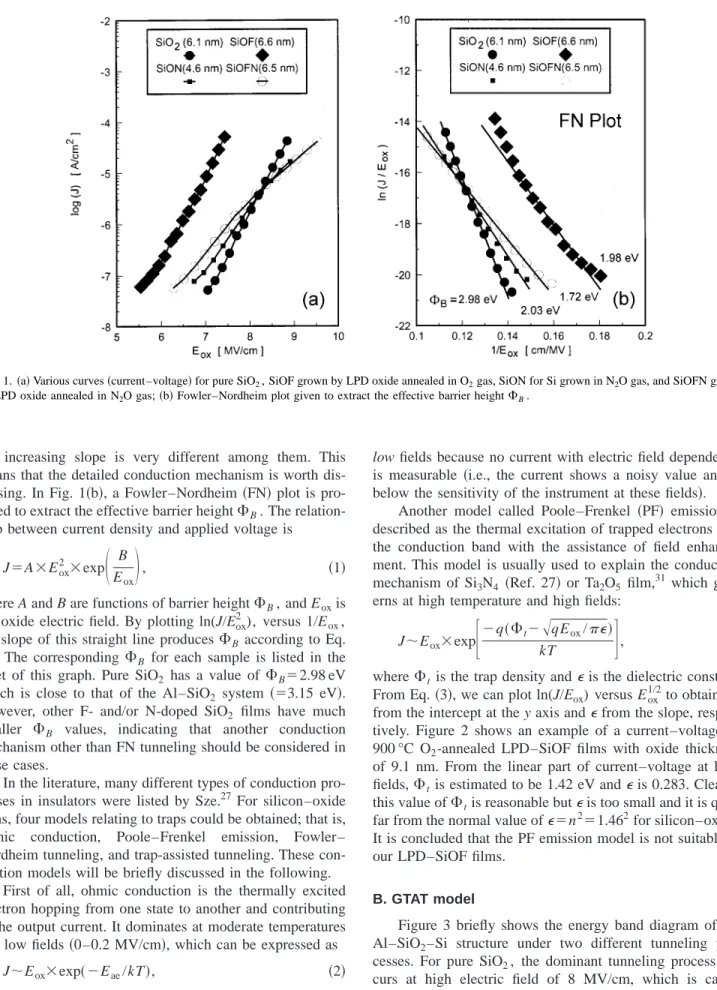
Figure 1 共a兲 shows the current–voltage curves of pure SiO
2, SiOF grown by LPD oxide annealed in O
2gas, SiON from Si grown in N
2O gas, and SiOFN grown by LPD oxide annealed in N
2O gas. Although the oxide thicknesses are not identical, we have shown them in this figure by normalizing them to get the corresponding electric fields. It is found that the leakage current increases with applied voltage, however,
TABLE I. Growth parameters of LPD process and annealings used in this study.
LPD growth time
共min兲
Initial oxide
thickness
共nm兲
Annealing in O2共°C, min兲
Annealing in N2O
共°C, min兲
Final oxide thickness
共nm兲
— — 900, 7 — 6.1
— — — 900, 25 4.6
5 1.9 900, 7 — 4.1
7.5 2.2 900, 7 — 4.9
10 3.4 900, 7 — 5.1
12.5 3.7 900, 7 — 5.9
10 1.9 850, 15 — 6.4
10 1.9 950, 5 — 7.4
10 1.8 900, 5 — 6.6
10 1.8 900, 10 — 7.0
10 1.8 900, 15 — 8.3
10 1.8 900, 20 — 9.1
10 2.5 — 900, 5 5.5
10 2.4 — 900, 10 6.2
10 2.2 — 900, 15 7.8
10 2.4 — 900, 20 8.6
5 2.5 — 900, 10 4.3
7.5 2.8 — 900, 10 5.7
10 3.2 — 900, 10 5.4
12.5 3.6 — 900, 10 6.5
5172 J. Appl. Phys., Vol. 90, No. 10, 15 November 2001 Chang, Houng, and Wang
the increasing slope is very different among them. This means that the detailed conduction mechanism is worth dis- cussing. In Fig. 1 共b兲, a Fowler–Nordheim 共FN兲 plot is pro- vided to extract the effective barrier height ⌽
B. The relation- ship between current density and applied voltage is
J ⫽A⫻E
ox2
⫻exp 冉 E B
ox冊 , 共1兲
where A and B are functions of barrier height ⌽
B, and E
oxis the oxide electric field. By plotting ln(J/E
ox2), versus 1/E
ox, the slope of this straight line produces ⌽
Baccording to Eq.
共1兲. The corresponding ⌽
Bfor each sample is listed in the inset of this graph. Pure SiO
2has a value of ⌽
B⫽2.98 eV which is close to that of the Al–SiO
2system 共⫽3.15 eV兲.
However, other F- and/or N-doped SiO
2films have much smaller ⌽
Bvalues, indicating that another conduction mechanism other than FN tunneling should be considered in these cases.
In the literature, many different types of conduction pro- cesses in insulators were listed by Sze.
27For silicon–oxide films, four models relating to traps could be obtained; that is, ohmic conduction, Poole–Frenkel emission, Fowler–
Nordheim tunneling, and trap-assisted tunneling. These con- duction models will be briefly discussed in the following.
First of all, ohmic conduction is the thermally excited electron hopping from one state to another and contributing to the output current. It dominates at moderate temperatures and low fields 共0–0.2 MV/cm兲, which can be expressed as
J ⬃E
ox⫻exp共⫺E
ae/kT 兲, 共2兲
where E
oxis the oxide field and E
aeis the activation energy of electrons. This model was also used to simulate the leak- age current at low fields in CVD–SiOF.
30In this case, by carefully observing the current–voltage of LPD–SiOF films, it can be seen that this model could not simulate current at
low fields because no current with electric field dependency is measurable 共i.e., the current shows a noisy value and is below the sensitivity of the instrument at these fields 兲.
Another model called Poole–Frenkel 共PF兲 emission is described as the thermal excitation of trapped electrons into the conduction band with the assistance of field enhance- ment. This model is usually used to explain the conduction mechanism of Si
3N
4共Ref. 27兲 or Ta
2O
5film,
31which gov- erns at high temperature and high fields:
J ⬃E
ox⫻exp 冋 ⫺q共⌽
t⫺ kT 冑 qE
ox/ ⑀ 兲 册 , 共3兲
where ⌽
tis the trap density and ⑀ is the dielectric constant.
From Eq. 共3兲, we can plot ln(J/E
ox) versus E
ox1/2to obtain ⌽
tfrom the intercept at the y axis and ⑀ from the slope, respec- tively. Figure 2 shows an example of a current–voltage of 900 °C O
2-annealed LPD–SiOF films with oxide thickness of 9.1 nm. From the linear part of current–voltage at high fields, ⌽
tis estimated to be 1.42 eV and ⑀ is 0.283. Clearly, this value of ⌽
tis reasonable but ⑀ is too small and it is quite far from the normal value of ⑀ ⫽n
2⫽1.46
2for silicon–oxide.
It is concluded that the PF emission model is not suitable to our LPD–SiOF films.
B. GTAT model
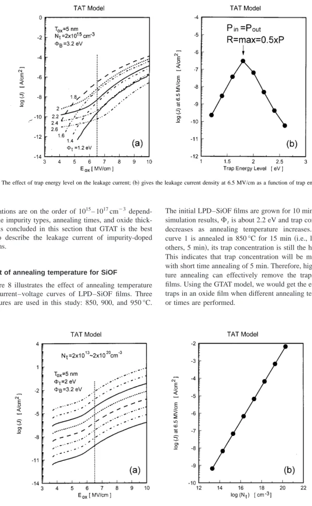
Figure 3 briefly shows the energy band diagram of the Al–SiO
2–Si structure under two different tunneling pro- cesses. For pure SiO
2, the dominant tunneling process oc- curs at high electric field of 8 MV/cm, which is called Fowler–Nordheim tunneling 共FNT兲. This has been verified by using curve fitting 共current–voltage兲 in Fig. 1共b兲. For the second case of the TAT process, the electrons tunneling from the left are injected into the traps existing in the oxide with tunneling probability P
in. Then these captured electrons are
FIG. 1.
共a兲 Various curves 共current–voltage兲 for pure SiO
2, SiOF grown by LPD oxide annealed in O2gas, SiON for Si grown in N2O gas, and SiOFN grown by LPD oxide annealed in N2O gas;共b兲 Fowler–Nordheim plot given to extract the effective barrier height ⌽
B.emitted again to tunnel through this oxide with tunneling probability P
out. In Fig. 3 it is found that the tunneling elec- trons meet either triangular barrier 关denoted as TAT共Tri.兲兴 or trapezoidal barrier 关denoted as TAT共Tra.兲兴 depending on the electric field across the oxide. In this model, we assume that the traps possess an energy level of ⌽
tbelow the oxide con- duction band and they are uniformly distributed all over the oxide. The relationship of J and E
oxcan be approximated as
J ⬃exp 冉 ⫺ 4 冑 2qm 3 ប
ox⌽
t3/2/E
ox冊 , 共4兲
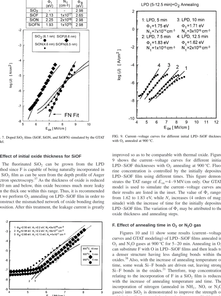
where ⌽
tcan be directly derived from the slope of the linear part in the ln(J) versus 1/E
oxplot. Figure 4 shows the TAT plot using our GTAT 共solid line兲 model, while the F–N fitted curve is also shown as a dashed line. ⌽
tis calculated to be 1.89 eV, ⌽
Bis 2.47 eV, and N
tis 6 ⫻10
16cm
⫺3. Note that
⌽
Bis an effective value that is different from 3.15 eV for Al–SiO
2. Obviously, the current–voltage curve at 5–9 MV/cm can be divided into two regions: TAT and FN tun- neling. Hence TAT with uniformly distributed trap concen- tration is the best model to explain the conduction mecha- nism in medium fields 共5–7 MV/cm兲.
C. Simulations of GTAT model
To have more insight into the effect of the trap energy level ⌽
tand trap concentration N
tfor current–voltage curves in the GTAT model, we have performed some simu- lations on devices having these parameters: ⌽
t⫽1.2– 2.6 eV, N
t⫽2⫻10
13– 2 ⫻10
20cm
⫺3, T
ox⫽5 nm, and
⌽
B⫽3.2 eV. Figure 5共a兲 shows the effect of trap energy level on the leakage current and Fig. 5 共b兲 presents the leak- age current density at 6.5 MV/cm as a function of the trap energy level. From this graph, it is clear that the leakage current increases with the increase of trap energy level from 1.2 to 1.8 eV to reach its maximum value and then decreases from 2 to 2.6 eV. Basically, the leakage current is changed by 3– 4 orders of magnitude in accordance with the variation of the trap energy levels. This particular phenomenon could also be seen in the ONO interpoly dielectric of erasable pro- grammable read-only memories.
32The maximum value at about 1.8 –1.9 eV is the result of tunneling-in probability ( P
in) ⫽tunneling-out probability (P
out). The tunneling rate R ⬀(P
in⫻P
out)/( P
in⫹P
out); therefore, it has a maximum value of 0.5 ⫻P.
Figure 6 共a兲 shows the effect of trap concentration on the leakage current and Fig. 6 共b兲 presents the leakage current density at 6.5 MV/cm as a function of trap concentration.
With the increase of trap concentration from 2 ⫻10
13to 2
⫻10
20cm
⫺3, the leakage current increases monolithically, indicating that trap concentration has a direct relationship with tunneling currents in an oxide film. In order to reduce the leakage current, traps existing in an oxide must be suffi- ciently reduced.
Since the current–voltage curves of doped SiO
2films 共SiOF, SiON, and SiOFN兲 could not be adequately modeled by FN tunneling, we use the GTAT model to simulate these curves and their results are shown in Fig. 7. The table in this figure presents some values obtained from the GTAT model.
One point worth noting is that the value of ⌽
textracted in our experiments is accepted when comparing it to other in- vestigators: 1.3–1.6 eV by Ramesh et al.,
232.46 –2.55 eV by Cheng et al.,
33and 2.1–2.7 eV by Fleischer et al.
34 –36Trap
FIG. 2. A current–voltage example of 900 °C O2-annealed LPD–SiOF films with 9.1 nm oxide thickness.
FIG. 3. Energy band diagram of Al–SiO2–Si structure under two different tunneling processes: FNT and TAT.
FIG. 4. TAT plot by our GTAT
共solid line兲 model for the sample in Fig. 3.
F–N fitted curve is also shown as dash line.
5174 J. Appl. Phys., Vol. 90, No. 10, 15 November 2001 Chang, Houng, and Wang
concentrations are on the order of 10
15– 10
17cm
⫺3depend- ing on the impurity types, annealing times, and oxide thick- ness. It is concluded in this section that GTAT is the best model to describe the leakage current of impurity-doped SiO
2films.
D. Effect of annealing temperature for SiOF
Figure 8 illustrates the effect of annealing temperature on the current–voltage curves of LPD–SiOF films. Three temperatures are used in this study: 850, 900, and 950 °C.
The initial LPD–SiOF films are grown for 10 min. From the simulation results, ⌽
tis about 2.2 eV and trap concentration decreases as annealing temperature increases. Although curve 1 is annealed in 850 °C for 15 min 共i.e., longer than others, 5 min 兲, its trap concentration is still the highest one.
This indicates that trap concentration will be much higher with short time annealing of 5 min. Therefore, high tempera- ture annealing can effectively remove the traps in oxide films. Using the GTAT model, we would get the evolution of traps in an oxide film when different annealing temperatures or times are performed.
FIG. 5.
共a兲 The effect of trap energy level on the leakage current; 共b兲 gives the leakage current density at 6.5 MV/cm as a function of trap energy level.
FIG. 6.
共a兲 The effect of trap concentration on the leakage current and 共b兲 gives the leakage current density at 6.5 MV/cm as a function of trap concentration.
E. Effect of initial oxide thickness for SiOF
The fluorinated SiO
2can be grown from the LPD method since F is capable of being naturally incorporated in the SiO
2film as can be seen from the depth profile of Auger electron spectroscopy.
37As the thickness of oxide is reduced to 10 nm and below, thin oxide becomes much more leaky than the thick one within this range. Thus, it is recommended that we perform O
2annealing on LPD–SiOF film in order to reconstruct the mismatched network of oxide bonding during deposition. After this treatment, the leakage current is greatly
improved so as to be comparable with thermal oxide. Figure 9 shows the current–voltage curves for different initial LPD–SiOF thicknesses with O
2annealing at 900 °C. Fluo- rine concentration is controlled by the initially deposited LPD–SiOF film using different times. This figure demon- strates the TAT range of E
ox⫽4–9 MV/cm only. Our GTAT model is used to simulate the current–voltage curves and their results are listed in the inset. The value of ⌽
tranges from 1.62 to 1.83 eV, while N
tincreases 共4 orders of mag- nitude 兲 with the increase of time for the initially deposited LPD–SiOF film. The variation of ⌽
tmay be attributed to the oxide thickness and annealing steps.
F. Effect of annealing time in O
2or N
2O gas
Figures 10 and 11 show some results 共current–voltage curves and GTAT modeling 兲 of LPD–SiOF films annealed in O
2and N
2O gases at 900 °C for 5–20 min. Annealing in O
2can substitute F with O in LPD–SiOF films and then leads to a denser structure having less dangling bonds within the oxides.
38Also, with the increase of annealing temperature or time, some weak Si–F bonds are driven out, leaving strong Si–F bonds in the oxides.
21Therefore, trap concentration relating to the incorporation of F in a SiO
2film is reduced with the increase of annealing temperature and time. The incorporation of nitrogen 共annealed in NH
3, NO, or N
2O gases 兲 into SiO
2is demonstrated to improve the strength of oxide’s bonding network by introducing strong Si–N bonds near the interface, and by increasing the endurance of trap creation.
39If nitrogen is introduced into a F-contained SiO
2system, a much more complex tetrahedral structure is
FIG. 7. Doped SiO2films
共SiOF, SiON, and SiOFN兲 simulated by the GTAT
model.FIG. 8. Effect of annealing temperature on the current–voltage curves for LPD–SiOF films. Three temperatures are used in this study: 850, 900, and 950 °C.
FIG. 9. Current–voltage curves for different initial LPD–SiOF thickness with O2annealed at 900 °C.
5176 J. Appl. Phys., Vol. 90, No. 10, 15 November 2001 Chang, Houng, and Wang
formed, F–Si 共O
3⫺xN
x), x ⫽0 – 3.
21In this article, our LPD–
SiOF films annealed in N
2O will become SiOF:N films. Of course it is evident that longer annealing time leads to smaller trap concentration due to the N passivation effect in the Si–O–Si bonding network. In this discussion, trap con- centrations between O
2- and N
2O-annealed LPD–SiOF films are compared.
For O
2annealing shown in Fig. 10, N
tdecreases from 8 ⫻10
17to 1 ⫻10
16cm
⫺3as the time is increased to 10 min.
After 15 min of annealing or more, GTAT could not be used to model the current–voltage curves. ⌽
Bis about 2.5 eV in this case. A second case for N
2O annealing is shown in Fig.
11: N
tis as low as 10
15cm
⫺3, 2 orders lower than that in O
2annealing. But ⌽
tis 1.24 and 1.85 eV for 5 and 10 min of annealing. These values of ⌽
t, different from the first case, may arise from the incorporation of N in LPD–SiOF film to change its energy level 共a combination of effects as a result of incorporating both nitrogen and fluorine 兲. After a long period of annealing 共15 and 20 min兲, ⌽
Bis similar to that in O
2annealing. These facts tell us that N
2O annealing could substantially decrease the traps contained in LPD–SiOF films. These N
2O annealed oxides show better electrical
properties than those of pure thermal oxides such as flatband voltage, interface trap density, and stress-induced gate volt- age shift.
40G. Effect of initial oxide thickness for SiOFN
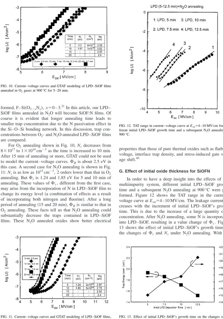
In order to have a deep insight into the effects of this multiimpurity system, different initial LPD–SiOF growth time and a subsequent N
2O annealing at 900 °C were per- formed. Figure 12 shows the TAT range in the current–
voltage curve at E
ox⫽4–10 MV/cm. The leakage current in- creases with the increment of initial LPD–SiOF’s growth time. This is due to the increase of a large quantity of F concentration. After N
2O annealing, some N is incorporated into LPD–SiOF, resulting in a value change of ⌽
t. Figure 13 shows the effect of initial LPD–SiOF’s growth time on the changes of ⌽
tand N
tunder N
2O annealing. With the
FIG. 10. Current–voltage curves and GTAT modeling of LPD–SiOF films annealed in O2gases at 900 °C for 5–20 min.
FIG. 11. Current–voltage curves and GTAT modeling of LPD–SiOF films, annealed in N2O gases at 900 °C for 5–20 min.
FIG. 12. TAT range in current–voltage curve at Eox
⫽4–10 MV/cm for dif-
ferent initial LPD–SiOF growth time and a subsequent N2O annealing at 900 °C.FIG. 13. Effect of initial LPD–SiOF’s growth time on the changes of
⌽
tand Ntunder N2O annealing.
increase of initial LPD–SiOF’s growth time, ⌽
tis decreased as shown by the solid squares. On the other hand, solid rhombuses reveal the increase of N
t. Some possible expla- nations could be described in the following.
For pure SiO
2, the bonding network of oxide is com- posed mainly of Si–O bonds with Si and O being tightly bonded to each other. There are very few traps existing in this type of oxide. If a foreign atom were incorporated 共for example, fluorine 兲, it would displace oxygen in a Si–O–Si bond and result in a dangling bond on the Si atom.
26Further- more, if another impurity such as nitrogen is introduced into a F-contained SiO
2system, a much more complex tetrahe- dral structure is formed, F–Si 共O
3⫺xN
x), x ⫽0 – 3.
21The con- centration of Si–F is slightly reduced because some weak Si–F bonds are removed and stronger Si–F are left in the oxide. With the initial LPD–SiOF thickness being thin 共hence smaller F concentration in quantity兲, the incorpora- tion of N would bond with F to produce a mixed effect, i.e.,
⌽
tis lowered. This type of trap energy level is called effec- tive ⌽
tbecause there are two atoms contributing to this pa- rameter. Furthermore, SiO
2containing F induces defects such as –Si–O–O–Si– structures.
22When F concentration is increased, the incorporation of N is insufficient to affect the large amounts of Si–F bonds, hence F is a dominant factor in this case, i.e., N
tis increased with growth time and ⌽
tis similar to that in SiOF film.
IV. CONCLUSION
For the increasing demand in quality of gate dielectrics other than conventional SiO
2, it is well know that adequately introducing fluorine or nitrogen atoms into SiO
2could im- prove the oxide properties for both Si–oxide interface and bulk oxide. SiOF and SiON films have received much atten- tion in the past 20 yr. However, SiOFN films demonstrate their potential for future gate dielectrics because of the ad- vantages described in Sec. I. Therefore, it is our motive to investigate the electrical properties of various doped SiO
2to obtain greater understanding.
First of all, the conduction mechanisms were discussed to determine which one was the best to explain the leakage current in these oxides. It was found that FNT could only model the current–voltage curve at high fields, where at moderate fields it could be well fitted by the TAT model. PF emission and ohmic conduction were excluded because they provide incorrect modeling results for current–voltage curves. Second, we have briefly discussed the GTAT model and used it to fit the current–voltage curves of doped oxides.
From the results acquired, ⌽
tcould be derived with the simple TAT plot using ln(J) versus 1/E
ox. Then, the simu- lated results of a trapped oxide with ⌽
t⫽1.2– 2.6 eV, N
t⫽2⫻10
13– 2 ⫻10
20cm
⫺3, T
ox⫽5 nm, and ⌽
B⫽3.2 eV were given to determine the suitability of this model. It was found that the leakage current has a maximum value at about 1.8 eV because tunneling-in probability is equal to tunneling-out probability. In the third part, the current–voltage modelings of SiOF and SiOFN films were investigated. The trap energy levels of SiOF films ranged from 1.62 to 2.2 eV, while trap concentrations were 7 ⫻10
14– 3 ⫻10
18cm
⫺3depending on
annealing temperature, time, and initial oxide thickness. An explicit effect of annealing on trap concentration was clearly observed. As for SiOFN films, the trap energy levels ranged from 1.24 to 2.25 eV, while trap concentrations were 5
⫻10
14– 3 ⫻10
20cm
⫺3depending on different annealing time and initial oxide thickness. By introducing N into the SiOF films, ⌽
tand N
twere significantly changed due to the for- mation of complex compounds of Si, O, F, and N in silicon dioxides. Some possible explanations were given to clarify this mixing effect. The results in this article provide a deeper insight into SiO
2containing impurities in terms of their elec- trical behaviors. It also provides a guideline on fabricating well-controlled dielectrics for future MOSFETs.
ACKNOWLEDGMENT
This work is supported by the National Science Council of the Republic of China under Contract No. NSC 88-2215- L006-032.
1S. W. Lim, Y. Shimogaki, Y. Nakano, K. Tada, and H. Komiyama, Jpn. J.
Appl. Phys., Part 1 35, 1468
共1996兲.
2U. S. Kim, C. H. Wolowoliuk, and R. J. Jaccodine, J. Electrochem. Soc.
137, 229
共1990兲.
3D. Kouvatsos, J. G. Huang, and R. J. Jaccodine, J. Electrochem. Soc. 138, 1752
共1991兲.
4Y. Nishioka, K. Ohyu, Y. Ohji, N. Natuaki, K. Mukai, and T. P. Ma, IEEE Electron Device Lett. 10, 141
共1989兲.
5K. Ohyu, T. Itoga, Y. Nishioka, and N. Natsuaki, Jpn. J. Appl. Phys., Part 1 28, 1041
共1991兲.
6Y. Nishioka, Y. Ohji, K. Mukai, T. Sugano, Y. Wang, and T. P. Ma, Appl.
Phys. Lett. 54, 1127
共1989兲.
7E. F. da Silva, Jr., Y. Nishioka, and T. P. Ma, IEEE Trans. Nucl. Sci.
NS-34, 1190
共1987兲.
8L. Vishnubhotla, T. P. Ma, H. H. Tseng, and P. J. Tobin, Appl. Phys. Lett.
59, 3595
共1991兲.
9H. Hwang, W. Tang, B. Maiti, D. L. Kwang, and J. Lee, Appl. Phys. Lett.
57, 1010
共1990兲.
10R. I. Hegde, B. Maiti, and P. J. Tobin, J. Electrochem. Soc. 144, 1081
共1997兲.
11M. Takayanagi-Takagi and Y. Toyoshima, IEEE International Electron De- vices Meeting, 1998, p. 575.
12M. Navi and S. T. Dunham, J. Electrochem. Soc. 145, 2545
共1998兲.
13T. Hori and H. Iwasaki, J. Appl. Phys. 65, 629
共1989兲.
14C. W. Chen, Y. K. Fang, K. Y. Lee, J. C. Hsieh, and M. S. Liang, Jpn. J.
Appl. Phys., Part 1 35, 2590
共1996兲.
15H. Nagayama, H. Honda, and H. Kawahara, J. Electrochem. Soc. 135, 2013
共1988兲.
16H. Fukuda, T. Arakawa, and S. Ohno, IEEE Trans. Electron Devices 39, 127
共1992兲.
17J. Kim, A. B. Joshi, G. W. Yoon, and D. L. Kwong, IEEE Electron Device Lett. 14, 265
共1993兲.
18M. Bhat, J. Kim, J. Yan, G. W. Yoon, L. K. Han, and D. L. Kwong, IEEE Electron Device Lett. 15, 421
共1994兲.
19J. G. Huang and R. J. Jaccodine, J. Electrochem. Soc. 140, L15
共1993兲.
20R. Swope, W. S. Yoo, J. Hsieh, S. Shuchmann, F. Nagy, H. te Nijenhuis, and D. Mordo, J. Electrochem. Soc. 144, 2559
共1997兲.
21S. Hasegawa, A. Saito, J. A. Lubguban, T. Inokuma, and Y. Kurata, Jpn. J.
Appl. Phys., Part 1 37, 4904
共1998兲.
22Y. Saito and U. Mori, Jpn. J. Appl. Phys., Part 2 37, L1172
共1998兲.
23K. Ramesh, A. N. Chandorkar, and J. Vasi, J. Appl. Phys. 65, 3958
共1989兲.
24S. K. Lai, D. W. Dong, and A. Hartstein, J. Electrochem. Soc. 129, 2042
共1982兲.
25S. T. Chang, N. M. Johnson, and S. A. Lyon, Appl. Phys. Lett. 44, 316
共1984兲.
26P. J. Wright and K. C. Saraswat, IEEE Trans. Electron Devices 36, 879
共1989兲.
27S. M. Sze, Physics of Semiconductor Devices, 2nd ed.
共Wiley, New York,
1981兲, p. 403.
5178 J. Appl. Phys., Vol. 90, No. 10, 15 November 2001 Chang, Houng, and Wang
28M. P. Houng, Y. H. Wang, and W. J. Chang, J. Appl. Phys. 86, 1488
共1999兲.
29W. J. Chang, M. P. Houng, and Y. H. Wang, J. Electrochem. Soc. 147, 3467
共2000兲.
30T. Homma, R. Yamaguchi, and Y. Murao, J. Electrochem. Soc. 140, 687
共1993兲.
31G. S. Oehrlein, J. Appl. Phys. 59, 1587
共1986兲.
32M. R. Herrmann, M. Ciappa, and A. Schenk, International Reliability Physics Symposium, 1994, p. 368.
33X. R. Cheng, Y. C. Cheng, and B. Y. Liu, J. Appl. Phys. 63, 797
共1988兲.
34S. Fleischer, P. T. Lai, and Y. C. Cheng, J. Appl. Phys. 72, 5711
共1992兲.
35S. Fleischer, P. T. Lai, and Y. C. Cheng, J. Appl. Phys. 73, 3348
共1993兲.
36S. Fleischer, P. T. Lai, and Y. C. Cheng, J. Appl. Phys. 74, 740
共1993兲.
37N. F. Wang, W. J. Chang, M. P. Houng, Y. H. Wang, and C. J. Huang, J.
Vac. Sci. Technol. A 17, 102
共1999兲.
38W. S. Lu and J. G. Hwu, IEEE Electron Device Lett. 17, 172
共1996兲.
39G. Q. Lo, W. C. Ting, D. K. Shih, and D. L. Kwong, Electron. Lett. 25, 1354
共1989兲.
40W. J. Chang, M. P. Houng, and Y. H. Wang, Jpn. J. Appl. Phys., Part I