Characterization of NH
3
plasma-treated Ba
0:7
Sr
0:3
TiO
3
thin ®lms
D.S. Wuu
a,*, R.H. Horng
b, F.C. Liao
a, C.C. Leu
c, T.Y. Huang
c, S.M. Sze
c,
H.Y. Chen
d, C.Y. Chang
daInstitute of Electrical Engineering, Da-Yeh University, Chang-Hwa 515, Taiwan, ROC bInstitute of Precision Engineering, National Chung Hsing University, Taichung 402, Taiwan, ROC
cNational Nano Device Laboratory, Hsinchu 300, Taiwan, ROC
dInstitute of Electrical Engineering, National Chiao Tung University, Hsinchu 300, Taiwan, ROC
Abstract
The eects of plasma surface treatment, using NH3gas, of Ba0:7Sr0:3TiO3(BST) ®lms on the leakage and dielectric
characteristics of a Pt/BST/Pt capacitor were investigated. As a result of the exposure of BST to the plasma, the leakage current density of the BST capacitor can be improved by three orders of magnitude as compared to that of the non-plasma-treated sample at an applied voltage of 1.5 V. Nevertheless, the surface morphology of BST was also changed by the NH3plasma, as explored by atomic force microscopy. From the X-ray photoelectron spectroscopy examination,
the existence of the N 1 s peak was observed in the plasma-treated sample. It induces the additional space charge and results in the reduction of the dielectric constant. Ó 2000 Elsevier Science Ltd. All rights reserved.
1. Introduction
The advancement of dynamic random access mem-ories (DRAMs) has signi®cantly decreased the available area per cell. Especially, Gbit-scale DRAMs require a very small SiO2equivalent thickness of less than 1 nm to
provide a sucient capacitance of 25 fF/cell in a cell size smaller than 0.1 lm2 [1]. The eort to shrink charge
storage devices has stimulated interest in high-dielectric-constant materials. Among the numerous ferroelectric materials, (Ba,Sr)TiO3 (BST) thin ®lms have attracted
considerable attention, because of its high dielectric constant, low leakage current density, high dielectric breakdown strength, paraelectric perovskite phase that does not exhibit fatigue, and the ease of composition control due to the absence of a volatile lead oxide [2±4]. Although the leakage and dielectric properties of BST ®lms have been proven to be excellent, they are highly thickness dependent [5,6]. The leakage current of BST
has been reported to drastically increase, when the ®lm thickness is reduced to less than 20 nm. It has been re-ported that an additional oxidation of a nitrided silicon dioxide can achieve the reduction of both electron trapping and interface-state generation [7±9]. The im-provement of interfacial quality has been attributed to nitrogen incorporation at the Si/SiO2 interface.
Nitri-dation of gate oxide ®lms with NH3 or N2O is an
ef-fective process in blocking impurity penetration and in reducing interface trap states. N2O-annealing and
plas-ma treatments have been employed to improve the properties of Ta2O5 and BST [10,11]. In this article, the
NH3 plasma eects on the leakage and dielectric
prop-erties of the BST ®lms were investigated. The material properties of BST modi®ed by the NH3plasma will also
be described.
2. Experimental
The BST thin ®lms with a Ba/Sr ratio of 70/30 were deposited on Pt(200 nm)/Ti(20 nm)/SiO2(250 nm)/Si
substrates using a spin-on sol±gel process. The coated ®lms were dried at 150°C for 5 min and pre-baked at
Microelectronics Reliability 40 (2000) 663±666
www.elsevier.com/locate/microrel
*Corresponding author. Tel.: +886-4-8528469, ext: 2168; fax: +886-4-8521904.
E-mail address: [email protected] (D.S. Wuu).
0026-2714/00/$ - see front matter Ó 2000 Elsevier Science Ltd. All rights reserved. PII: S 0 0 2 6 - 2 7 1 4 ( 9 9 ) 0 0 3 1 4 - 5
400°C for 20 min. This procedure was repeated four times and the 100-nm-thick BST thin ®lm was obtained. The as-deposited BST ®lms were subjected to three kinds of process treatment. One set of samples was di-rectly treated by thermal annealing without plasma treatment. They were used as the ``reference'' samples for the aim of measurement comparison. The second set of samples was ®rst annealed and followed by NH3
plasma treatment (anneal before plasma, ABP) for 30, 60 and 120 s. They were correspondingly denoted by NH3-30, NH3-60 and NH3-120, respectively. The third
set of samples was exposed to the NH3plasma for 30, 60
and 120 s and then thermal annealed (anneal after plasma, AAP). They were correspondingly denoted by NH3-B30, NH3-B60 and NH3-B120. The anneal for
these BST ®lms was carried out in a puri®ed O2
atmo-sphere at 700°C for 1 h. During the plasma treatment, the substrate temperature, chamber pressure and RF power were maintained at 250°C, 300 mTorr and 200 W, respectively.
All the leakage and dielectric characteristics were measured using the metal±insulator±metal structure with Pt as the top and bottom electrodes. The top electrodes with diameter of 300 lm were formed by sputtering and patterned by the shadow mask process. The leakage current density versus dc voltage (J±V) was measured by HP 4145B. The capacitance versus dc voltage (C±V) was measured at 100 kHz using a Ke-ithley CV 82 analyzer with an oscillation voltage at 50 mV. The chemical compositions of samples were ex-amined by X-ray photoelectron spectroscopy (XPS). The surface morphology of the BST ®lm was observed by an atomic force microscope (AFM).
3. Results and discussion
Fig. 1(a) and (b) shows the J±V curves of the BST ®lms treated by AAP and ABP processes, respectively. The data taken from the reference sample are also de-picted for comparison. It was found that the plasma-treated BST ®lms (AAP or ABP) showed lower leakage levels than the reference sample, except for the NH3-30
sample. Further, the leakage current density of the AAP sample is lower than that of ABP sample. The leakage current density was found to decrease as the plasma-treated duration increased. Notably, except for the ref-erence and NH3-30 samples, the leakage current density
of the BST ®lm under a negative bias is slightly higher than that under a positive bias. Fig. 2 shows the di-electric constant (e) as a function of voltage for the plasma-treated and reference samples. It was found that the dielectric constants for these samples are as follows: e referencesample > e ABPsample > e AAPsample. The lower dielectric constants of the plasma-treated ®lms imply that the BST ®lms are damaged by the
ex-posure of the BST surface to the plasma. For the AAP samples, the ®lm structure of BST was amorphous as exposed to the plasma. Thus, they are more easily at-tacked by plasma as compared with the ABP samples. This results in a lower e value of the AAP sample. Nevertheless, the dissipation factors are obviously re-duced by 50±70% by the plasma treatment, as shown in the Fig. 3. For the AAP samples, the dissipation factor
Fig. 1. J±V curves of the reference samples and compared with the BST ®lms treated by (a) thermal annealing before NH3 plasma, and (b) thermal annealing after NH3plasma.
Fig. 2. Dielectric constant as a function of applied voltage for the reference and NH3plasma-treated samples.
decreases slowly as the plasma-treated duration in-creases. It could be due to the fact that the thermal annealing can rearrange the surface morphology after the plasma treatment.
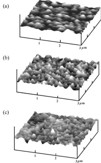
The surface morphology of BST is an important factor in consideration of the conduction mechanism. The AFM topographies of the reference, ABP (NH3
-120) and AAP (NH3-B120) samples are shown in Fig. 4.
The corresponding surface roughness for these samples is 1.041, 1.398 and 1.428 nm, respectively. For the ref-erence sample, AFM revealed that grains merged to-gether. However, for the plasma-treated samples, the surface presents needle-like morphology due to the plasma bombardment. During the AAP treatment, the ®lm structure of BST was amorphous as exposed to the plasma. Although the needle-like structure can be smoothed by post-annealing, the AAP sample still has the greatest roughness among three sets of samples. Thus, the plasma eect for the AAP samples is larger than that for the ABP samples. Nevertheless, the an-nealing process will bene®t the surface morphology and make it smoother. The rounded surface morphology for the AAP samples may also result in the reduction of leakage current density. Moreover, the surface rough-ness also enlarges the capacitor electrode area, which could be one of the factors aecting the properties of the ®lms. The roughness for the AAP sample is more than that of the ABP sample; however, the e value for the AAP sample is lower than that of ABP samples. The eect of surface roughness seems to be negligible in this study. The plasma-treated BST ®lms with lower e values may be due to the nitrogen space charge accumulation (this point will be further discussed by XPS observa-tion). This suggests that nitrogen incorporation into the BST thin ®lms is more obvious for the AAP samples.
The result is consistent with the leakage behavior as described in Fig. 2.
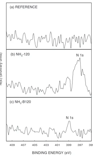
The nitrogen incorporation into the BST ®lms can be con®rmed by the XPS measurement, as shown in Fig. 5. No nitrogen signal can be detected in the reference sample. It was found that the N 1 s peak obviously ex-isted in the plasma-treated BST ®lms. The nitrogen in-corporation into the AAP samples is expected to be easier than that into the ABP samples. Note that the AAP treatment will activate and redistribute the nitro-gen into the BST thin ®lms. It would result in the surface nitrogen concentration lower than that of the ABP sample. The nitrogen incorporation will reduce the electron traps and interface states, and it will improve the leakage current performance. This can be supported by the evident reduction of leakage current density in the AAP samples. Typically, the leakage current den-sity of the NH3-B120 sample decreases by three orders
of magnitude as compared with that of the reference
Fig. 3. Dissipation factor as a function of plasma-treated du-ration for the BST samples. The arrow indicates the dissipation factor of the reference sample.
Fig. 4. AFM topographies of the (a) reference sample, (b) NH3-120 sample and (c) NH3-B120 sample.
sample at an applied voltage of 1.5V. But the annealing process for the AAP samples would make the space charge range widen, which results in lowering the di-electric constant.
4. Conclusions
The BST ®lms with a 100 nm thickness were pre-pared by spin coating onto Pt(150 nm)/Ti(20 nm)/
SiO2(200 nm)/Si substrate. Both BST ®lms before and
after thermal anneal were then exposed to RF plasma using NH3 as the source gas. It is found that the NH3
plasma treatment results in the reduction of leakage current of BST ®lms. When the plasma-treated duration increases, the leakage current density decreases. Typi-cally, the leakage current density can decrease by three orders of magnitude as compared that of the non-plasma treated sample at an applied voltage of 1.5V. The AFM shows that the surface morphology of BST ®lms was changed by plasma treatment and the AAP samples have greater roughness. For the samples treated by NH3plasma, the dielectric constant were reduced by
10±40%. Nitrogen accumulation induced by plasma bombardment may be the main eect, which results in the reduction of dielectric constant. It is necessary to trade o the capacitance property for leakage current property.
References
[1] Yamamichi S, Yamamichi A, Park D, King TJ, Hu C. IEEE Trans Electron Devices 1999;46:342.
[2] Horikawa T, Mikami N, Makita T, Tanimura J, Kataoka M, Sato K, Nunoshita M. Jpn J Appl Phys 1993;32:4126.
[3] Chen PO, Miki H, Shimamoto Y, Matsui Y, Hiratani M, Fujisaki Y. Jpn J Appl Phys 1997;37:5112.
[4] Kuoiwa T, Tsunenine Y, Horikawa T, Makita T, Tanimura J, Mikami N, Sato K. Jpn J Appl Phys 1994;33:5187.
[5] Roy D, Krupanidhi SB. Appl Phys Lett 1993;62:1056. [6] Hwang CS, Park SO, Cho HJ, Kang CS, Kang HK, Lee SI,
Lee MY. Appl Phys Lett 1995;67:2819.
[7] Park SO, Hwang CS, Cho HJ, Kang CS, Kang HK, Lee SI, Lee MY. Jpn J Appl Phys 1996;35:233.
[8] Hori T, Iwasaki H, Tsuji K. IEEE Trans Electron Devices 1989;36:340.
[9] Ito T, Nakamura T, Ishikawa H. IEEE Trans Electron Devices 1982;29:498.
[10] Moslehi MM, Saraswat KC. IEEE Trans Electron Devices 1985;32:106.
[11] Sun SC, Chen TF. IEEE Electron Devices Lett 1996;17:355.
Fig. 5. XPS spectra of the (a) reference sample, (b) NH3-120 sample and (c) NH3-B120 sample.