Planar GaN
n
¿–
p
photodetectors formed by Si implantation into
p
-GaN
J. K. Sheu,a)M. L. Lee,b)L. S. Yeh, C. J. Kao, C. J. Tun,c)M. G. Chen, G. C. Chi,S. J. Chang,b) Y. K. Su,b) and C. T. Leec)
Department of Physics, National Central University, Chung-Li 320, Taiwan, Republic of China 共Received 6 May 2002; accepted 7 October 2002兲
GaN n⫹– p junction diodes were fabricated by implanting Si atoms into p-GaN. It was shown that we could use these diodes as GaN-based planar photodetectors. It was found that the dark current density of the diodes was around 1.5 A/cm2 and 50 nA/cm2 at reverse biases of 3 and 1 V, respectively. Spectra response measurements revealed a cutoff wavelength at around 365 nm and a peak responsivity of 0.33 mA/W at 365 nm for the GaN planar n⫹– p photodetectors. It was also found that the visible rejection ratio was around 260. Furthermore, temporal response measurements revealed that the fall times of these GaN planar n⫹– p photodetectors were found to be shorter than 0.4s. © 2002 American Institute of Physics. 关DOI: 10.1063/1.1524689兴
III-nitride semiconductors are highly promising for the fabrication of electronic devices operating at high tempera-tures owing to their superior physical properties, such as wide band gap, high breakdown field, and high thermal con-ductivity. These semiconductors have been used to fabricate UV photodetectors.1–7An ideal UV photodetector should be insensitive to visible and IR background. Typical values of UV-to-visible rejection ratio, which is the ratio of photore-sponse in UV region to photorephotore-sponse in visible region, are about three to four orders of magnitude for GaN-based UV photodetectors, such as p – i – n photodiodes and Schottky barrier photodetectors.1–7 Compared with Schottky barrier photodetectors, p – n junction photodetectors have a high breakdown voltage, a fast response speed, a sharp cutoff, and a high responsivity. These advantages all make p – n junction photodetectors attractive for practical applications. However, most GaN-based devices are grown on top of insulating sap-phire substrates. Thus, it is always necessary to etch away part of the sample surface so as to fabricate a conventional GaN-based p – n junction photodetector. In other words, con-ventional GaN-based p – n junction photodetectors are non-planar. Such a nonplanarity could result in at least a draw-back in photodetectors. For example, leakage current might increase with the perimeter of device due to surface recom-bination resulting from etched surface. Previously, we have reported the fabrication of GaN n⫹– p junction diodes formed Si implantation into p-GaN.8 It has been shown that we could achieve a planar GaN p – n junction with reason-ably good electrical properties. In this study, we demon-strated planar GaN n⫹– p photovoltaic detectors fabricated by Si implantation into p-GaN.
Prior to Si ion implantation, Mg-doped GaN samples were first grown on c-face sapphire substrates by metalor-ganic vapor phase epitaxy. Details of the GaN growth proce-dures have already been described elsewhere.9 Hall-effect measurement showed that hole concentration and hole mo-bility of the as-grown p-type GaN was 3⫻1017 cm⫺3and 12
cm2/V s, respectively. In this study, triple28Si⫹implantation
was performed to convert p-type GaN into n-type GaN films. According to our previous experiences, single dose/energy implantation (5⫻1015 cm⫺2/150 KeV兲 will result in a non-uniform Si doping profile and thus a larger error in Hall-effect measurements. Therefore, triple implantation was per-formed to form a Si-implanted layer with uniform doping profile. The triple implantation condition 共dose/energy兲 is 3.8⫻1014cm⫺2/40 keV, 6.8⫻1014 cm⫺2/100 keV, and 1.5 ⫻1015 cm⫺2/150 keV. The overall implantation depth was
estimated to be about 0.2 m. The as-implanted samples were then thermal annealed at 1100 °C for 60 s. It was found that we could successfully convert p-GaN into n⫹-GaN by Si implantation and annealing. The electron concentration of the implanted n⫹-GaN layer was around 3⫻1018 cm⫺3, as determined by Hall-effect measurements. Si-implanted GaN n⫹– p junction diodes were then fabricated by depositing n-and p-ohmic contacts onto the same upper surface of the samples. Ti/Al/Pt/Au 共30/100/50/150 nm兲 and Ni/Au 共4/10 nm兲 deposited by e-beam evaporator followed by N2-ambient thermal alloying were used as the contact
mate-rials for n⫹-GaN and p-GaN, respectively. Detailed fabrica-tion processes of such GaN n⫹– p planar junction diodes were also described elsewhere.8
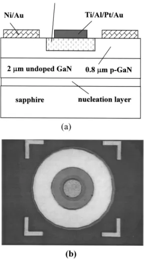
Figures 1共a兲 and 1共b兲 show the schematic device struc-ture and photograph of the real device, respectively. Room temperature current–voltage (I – V) characteristics of these diodes were then measured using an HP4145B semiconduc-tor parameter analyzer. Spectral responsivity of the Si-implanted planar n⫹– p photodetector was also measured us-ing a Xe arc lamp and a calibrated monochromator as the light source. The power of the monochromatic light was measured with a calibrated silicon photodiode and then illu-minated onto the front side of the photodetectors. During transient time measurement, a pulse N2 laser emitting at 337 nm was used as the excitation source. The pulse width of the laser was 0.5 ns. A 500 MHz oscilloscope with a 1000 ⍀ load resistance was used to measure the photocurrent gener-ated by the nonbiased GaN photodetectors under pulse N2
laser illumination.
For detector applications, electrical property of the junc-tion diodes in the reverse-bias situajunc-tion is very critical. For example, high leakage current 共dark current兲 would reduce
a兲Electronic mail: [email protected]
b兲Institute of Microelectronics, Department of Electrical Engineering,
Na-tional Cheng Kung University Tainan 70101, Taiwan, Republic of China. c兲Institute of optical Science, National Central University, Chung-Li 320,
Taiwan, Republic of China.
APPLIED PHYSICS LETTERS VOLUME 81, NUMBER 22 25 NOVEMBER 2002
4263
0003-6951/2002/81(22)/4263/3/$19.00 © 2002 American Institute of Physics
the sensitivity of photodetectors and thus reduce signal-to-noise ratio 共SNR兲. On the other hand, one can extract the series resistance of GaN n⫹– p photodetectors from its I – V characteristics. A large series resistance will significantly re-duce the operation speed of the photodetectors. Series resis-tance came mainly from contact resisresis-tance of electrodes and sheet resistance in the p-GaN layer.10
Here, we would like to concentrate our attention on the discussion of dark current. Figure 2 shows a typical I – V characteristic of Si-implanted GaN n⫹– p photodetectors. It was found that dark current density was around 1.5 and 50
nA/cm2when the photodetector was reverse biased at 3 and 1 V, respectively. It was also found that when the reverse bias was smaller than 2 V, the reverse dark current density was smaller than 10⫺7A/cm2. However, the reverse dark current density increased drastically when the reverse bias became larger than 2 V. This dark current was higher than the re-ported values observed from p – i – n diodes prepared by epi-taxially lateral overgrown GaN.1,11,12 This might be due to the presence of trap levels within the band gap of our samples, which give rise to a high leakage current. These levels are most likely associated either with process damage or with structural defects, including point defects.
It is known that defects in GaN 共i.e., dislocation origi-nating from large lattice mismatch between sapphire and GaN兲 can reveal themselves in high leakage currents.13 In this case, the implanted damage would also play an impor-tant role in the origins of trap levels and hence leakage cur-rent. In addition, traps within band gap might also cause the slow transient response of photodetectors. It is worth noting that further analyses, such as temperature-dependent electri-cal characterization, are needed to clarify the charged state of trap and to extract the trap density. A detailed study on the implantation induced trap levels will be reported elsewhere. Figure 3 shows the spectral responsivity of the Si-implanted planar n⫹– p photodetectors under reverse bias. It was found that cutoff occurred at around 365 nm. Theoreti-cally, when the incident photon energy is greater than GaN band-gap energy, all optical energy is absorbed, and in turn transfers to photocurrent. As shown in Fig. 3, one can ob-served a significant decrease rather than a flat response when the incident wavelength is shorter than 365 nm. This phe-nomenon can be attributed to the absorption in the n⫹-GaN layer. Thus, only few photons are absorbed in the depletion layer where photocurrent is generated. GaN has a very high absorption coefficient (⬎105 cm⫺1) for high energy 共short
wavelength兲 photons. Thus, the penetration depth is only around 0.1m for the high energy photons (ប⬃3.4 eV). 14 For this reason, if a Si-implanted planar GaN n⫹– p photo-diode is to have a broad spectral responsivity, it should have a very thin n⫹-GaN layer to allow penetration of short-wavelength (⬍365 nm) photons, since high energy pho-tons are mostly absorbed by the n⫹-GaN layer.
Since the thickness of n⫹-GaN layer used in this study is about 0.2m, minority carriers generated in this n⫹-GaN layer will recombine immediately before reaching the deple-FIG. 1. 共a兲 Schematic device structure shown in cross-section view. 共b兲
Photograph of a Si-implanted n⫹– p junction diode with a concentric-circle configuration.
FIG. 2. Logarithmic current–voltage characteristics of one of these Si-implanted n⫹– p GaN photodiodes.
FIG. 3. Spectral responsivity of the typical Si-implanted planar n⫹– p ul-traviolet detector with reverse bias of 1 and 3 V.
4264 Appl. Phys. Lett., Vol. 81, No. 22, 25 November 2002 Sheuet al.
tion region. Thus, only photons with energy close to GaN band-gap energy can reach deeper to produce electron–hole pairs in the depletion region. On the other hand, we could maximize photocurrent by increasing depletion width. The depletion width depends on both material resistivity of the region to be depleted and the applied reverse bias. In other words, we could increase depletion width by choosing high resistive 共i.e., low doping兲 materials on both sides of the junction. However, low resistivity materials are required for the formation of good n- and p-ohmic contacts. Thus, we might need a high reverse bias to extend the depletion re-gion.
As shown in Fig. 3, it was found that the maximum responsivity of the planar GaN n⫹– p was around 0.33 mA/W at 365 nm. It was also found that the visible rejection ratio was around 260. These values are smaller than those reported from epitaxially grown GaN p – i – n photodetectors.1–5 This can be attributed to the following reasons. First of all, the depletion width of Si-implanted pla-nar GaN n⫹– p photodetectors is normally smaller than that of epitaxial p – i – n photodetectors, since the active layer
共i.e., i-layer兲 of epitaxial p – i – n photodetectors can be well
controlled and fully depleted under suitable reverse bias. The defect density in Si-implanted planar GaN n⫹– p photodetectors is also larger due to the incomplete removal of implantation induced structural defects. The low peak re-sponsivity could be also attributed to the nonoptimum design of device geometry. In other words, only a small active area was illuminated during responsivity measurement, as shown in Fig. 1. In addition, the reflection loss of incident light at the air/GaN interface should also be considered. Thus, we should be able to increase the photodetector’s performance by a properly designed structure and the introduction of an-tireflection coating.
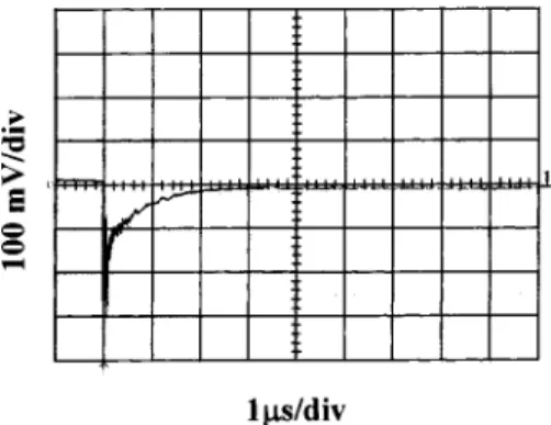
Figure 4 shows a typical transient response when the GaN planar n⫹– p photodetector was excited by pulse N2
laser. It is known that the rise time of a photodetector is limited by共i兲 the transit time of carrier drift across depletion region, tc, and 共ii兲 the time of carrier diffuse to junction
depletion region, td. In general, the rise time strongly
de-pends on defect density and impurity level in the semicon-ductor material. On the other hand, the fall time is mainly governed by the RC time constant, tRC, associated with
cir-cuit parameters, including junction capacitance C, diode re-sistance, and load resistance. Therefore, transient response time is governed by ⫽(tc2⫹td2⫹tRC2 )1/2.15
In our experiment, it was found that the measured fall times were all around 0.4s. It was also found that the fall times were also independent of the applied reverse bias. In theory, transient response will become faster with the in-crease of reverse bias, since the extended depletion region will reduce the junction capacitance. The fact that the tran-sient response is independent of applied revise bias suggests that fall time of our GaN planar n⫹– p photodetector is en-tirely limited by RC time constant of the detection circuit. Thus, the actual fall times of the devices should be smaller than 0.4 s, and it is necessary to use a high-performance apparatus to redo the transient response measurements so as to accurately determine the actual fall times. Further studies, which include the optimization of sample geometry and de-vice processing technology, are also needed to optimize the performance of such GaN planar n⫹– p photodetectors.
In summary, GaN n⫹– p junction diodes were fabricated by implanting Si atoms into p-GaN. It was shown that we could use these diodes as GaN-based planar photodetectors. It was found that the dark current density of the diodes was around 1.5A/cm2and 50 nA/cm2at reverse biases of 3 and 1 V, respectively. Spectra response measurements revealed a cutoff wavelength at 365 nm and a peak responsivity of 0.33 mA/W at 365 nm for the GaN planar n⫹– p photodetectors. It was also found that the visible rejection ratio was around 260. Furthermore, the fall times of these GaN planar n⫹– p photodetectors were found to be shorter then 0.4s.
The authors would like to acknowledge the financial support from the National Science Council for their research Grant No. NSC 90-2215-E-008-043 and NSC 90-2112-M-008-046.
1G. Parish, S. Keller, P. Kozodoy, J. P. Ibbetson, H. Marchand, P. T. Fini, S. B. Fleischer, S. P. DenBaars, U. K. Mishra, and E. J. Tarsa, Appl. Phys. Lett. 75, 247共1999兲.
2
J. Z. Li, J. Y. Lin, H. X. Jiang, and M. A. Khan, Appl. Phys. Lett. 72, 2868 共1999兲.
3M. A. Saleh, M. M. Hayat, O.-H. Kwon, A. L. Holmes, Jr., J. C. Campbell, B. E. A. Saleh, and M. C. Teich, Appl. Phys. Lett. 79, 4037共2001兲. 4M. A. Khan, J. N. Kkuznia, D. T. Olson, and M. Blasingame, Appl. Phys.
Lett. 63, 2455共1993兲.
5D. Walker, A. Saxler, P. Kung, X. Zhang, M. Hamilton, J. Diaz, and M. Razeghi, Appl. Phys. Lett. 72, 3303共1996兲, and references therein. 6Q. Chen, J. W. Yang, A. Osinsky, S. Gangopadhyay, B. Lim, M. Z. Anwar,
M. Asif Khan, D. Kuksenkov, and H. Temkin, Appl. Phys. Lett. 70, 2277 共1997兲.
7A. Osinsky, S. Gangopadhyay, J. W. Yang, R. Gaska, D. Kuksenkov, H. Temkin, I. K. Shmagin, Y. C. Chang, J. F. Muth, and R. M. Kolbas, Appl. Phys. Lett. 72, 551共1998兲.
8
J. K. Sheu, C. J. Tun, M. S. Tsai, C. C. Lee, G. C. Chi, S. J. Chang, and Y. K. Su, J. Appl. Phys. 91, 1845共2002兲, and references therein. 9J. K. Sheu, Y. K. Su, G. C. Chi, M. J. Jou, C. M. Chang, C. C. Liu, and W.
C. Hung, Appl. Phys. Lett. 74, 2340共1999兲.
10M. L. Lee, J. K. Sheu, L. S. Yeh, M. S. Tsai, C. J. Kao, C. J. Tun, S. J. Chang, and G. C. Chi, Solid-State Electron.共in press兲.
11J. C. Carrano, T. Li, P. A. Grudowski, C. J. Eiting, D. Lambert, J. D. Schaub, R. D. Dupuis, and J. C. Compbell, Electron. Lett. 34, 692共1998兲. 12W. Yang, T. Nohova, S. Krishnankutty, R. Torreano, S. Mcpherson, and H.
Marsh, Appl. Phys. Lett. 73, 1086共1998兲. 13
P. Kozodoy, J. P. Ibbetson, H. Marchand, P. T. Fini, S. Keller, J. S. Speck, S. P. DenBaars, and U. K. Mishra, Appl. Phys. Lett. 73, 975共1998兲. 14X. Zhang, P. Kung, D. Walker, J. Piotrowski, A. Rogalski, A. Saxler, and
M. Razeghi, Appl. Phys. Lett. 67, 2028共1995兲. 15
David Wood, Optoelectronic Semiconductor Devices共Prentice Hall, Lon-don, 1994兲.
FIG. 4. Typical transient response of fall time measured at a reverse bias of 0 V.
4265 Appl. Phys. Lett., Vol. 81, No. 22, 25 November 2002 Sheuet al.