Mechanism and lifetime prediction method for hot-carrier-induced
degradation in lateral diffused metal-oxide-semiconductor transistors
Jone F. Chen,1,a兲 Kuen-Shiuan Tian,1Shiang-Yu Chen,1J. R. Lee,1Kuo-Ming Wu,2and C. M. Liu2
1
Institute of Microelectronics, Department of Electrical Engineering, and Advanced Optoelectronic Technology Center, National Cheng Kung University, Tainan 70101, Taiwan
2
Taiwan Semiconductor Manufacturing Company, Hsinchu 30077, Taiwan
共Received 13 May 2008; accepted 29 May 2008; published online 16 June 2008兲
The mechanism of hot-carrier-induced degradation in n-type lateral diffused metal-oxide-semiconductor 共LDMOS兲 transistors is investigated. Experimental data reveal that hot-electron injection induced interface state generation in channel region is the main degradation mechanism. Since gate current 共Ig兲 consists mainly of electron injection, Ig correlates well with device degradation. As a result, a lifetime prediction method based on Ig is presented for the purpose of projecting hot-carrier lifetime in LDMOS transistors. © 2008 American Institute of Physics. 关DOI:10.1063/1.2947588兴
Lateral diffused metal-oxide-semiconductor 共LDMOS兲 transistors have been widely used in many integrated smart-power applications because of their compatibility with stan-dard complementary metal-oxide-semiconductor 共CMOS兲 process. Because LDMOS devices are usually operated un-der high voltages, hot-carrier-induced degradation may be-come a serious reliability concern. To achieve a wide variety of high-voltage applications, LDMOS devices differ in de-vice design significantly. Thus, hot-carrier-induced degrada-tion in LDMOS transistors is more complicated than that in low-voltage metal-oxide-semiconductor field-effect transis-tors共MOSFETs兲. Several papers have reported that the deg-radation behavior in LDMOS transistors is quite different from that in MOSFETs.1–5To evaluate hot-carrier reliability of the device, it is crucial to identify the degradation mecha-nism and predict hot-carrier lifetime of the device. In this letter, hot-carrier-induced degradation in n-type LDMOS transistors is investigated. Experimental results reveal that device degradation is induced by interface state共Nit兲 genera-tion resulting from hot-electron injecgenera-tion in channel region. In addition, gate current共Ig兲 correlates well with device deg-radation. Finally, a lifetime prediction method based on Igis presented for the purpose of projecting hot-carrier lifetime in our LDMOS devices.
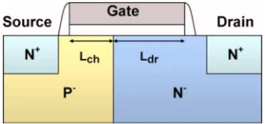
The schematic cross section of the n-type LDMOS tran-sistor used in this letter is shown in Fig. 1. This device is fabricated with a modified 0.25m CMOS process and fea-tures a n− drift region near the drain. The channel region 共Lch兲 and drift region 共Ldr兲 are indicated in the figure. Lchis about 0.5m and Ldr is roughly 0.7m. The gate oxide thickness and width of the device are 30 nm and 20m, respectively. The operational voltage of the device is 12 V for both drain voltage共Vds兲 and gate voltage 共Vgs兲. dc stress-ing under Vds= 13.2 V and various Vgs 共6, 9, and 12 V兲 is performed at room temperature. To evaluate hot-carrier-induced interface state generation 共⌬Nit兲, charge pumping technique similar to the method proposed in Ref.6is carried out during stressing. The stress tests are interrupted periodi-cally to measure the degradation of device parameters
关in-cluding on-resistance 共Ron兲 and maximum transconductance 共Gmmax兲兴 and charge pumping current 共Icp兲. Ronis measured under Vds= 0.1 V and Vgs= 12 V, while Gmmax is extracted under Vds= 0.1 V.
Figure2 shows substrate current共Isub兲 and Igas a func-tion of Vgsfor the device biased at Vds= 13.2 V. Only one Isub maximum occurs at Vgs⬇Vds/2, which is similar to the be-havior in MOSFETs. Ig increases monotonically and its maximum occurs at Vgs= 12 V, indicating that more elec-trons are injected into gate as Vgsincreases. In Fig.3, Ronand
Gmmaxdegradation as a function of Vgsduring stressing共6, 9, and 12 V兲 are examined for devices stressed under Vds = 13.2 V for 3000 s and two observations are found. First, the device stressed under higher Vgsproduces greater device degradation. This trend is different from that in MOSFETs, where hot-carrier-induced degradation is closely related to
Isub and the device with larger Isub is expected to produce greater device degradation.7–10However, data in Fig.3show that the Vgs to produce the most device degradation 共Vgs = 12 V兲 matches with the Vgs to produce Ig maximum rather than the Vgsto produce Isubmaximum. Such a result suggests that Igis a potential monitor to judge the severity of device degradation. Second, under the same Vgs during stressing,
Gmmax degradation is much greater than Ron degradation. Such a result reveals that hot-carrier-induced damage is mainly located in channel region rather than n− drift region since Gmmaxdegradation is attributed to the decrease in chan-nel mobility caused by⌬Nitin Si/SiO2interface.7
To evaluate hot-carrier-induced ⌬Nit in our LDMOS transistors, charge pumping measurement is performed. The
a兲Electronic mail: [email protected].
FIG. 1.共Color online兲 Schematic cross section of the n-type LDMOS device used in this letter. The channel region共Lch兲 and drift region 共Ldr兲 are indi-cated in the figure.
APPLIED PHYSICS LETTERS 92, 243501共2008兲
0003-6951/2008/92共24兲/243501/3/$23.00 92, 243501-1 © 2008 American Institute of Physics
pulse with a fixed high level共Vh兲 and a variable base level 共Vb兲 at a frequency of 500 kHz is applied to the gate. From technology computer-aided-design simulation results 共under
Vds= 0 V兲, flatband voltage 共Vfb兲, and threshold voltage 共VT兲 along Si/SiO2 interface can be extracted. Vfb is from 0.3 to − 1 V in Lchregion and from −1 to − 2.5 V in Ldr re-gion. VT is from 1.9 to 0 V in Lch region and from 0 to − 1 V in Ldr region. As a result,⌬Nit located in channel re-gion can be sensed when Vh= 4 V and Vb is varied from −1 to 3.5 V. ⌬Nit in drift region can be sensed when Vh = 0 V and Vbis varied from −3 to − 0.5 V. Thus,⌬Nitcan be extracted from charge pumping data by
⌬Nit= ⌬Icp
qfWLcp, 共1兲
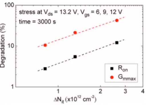
where⌬Icpis hot-carrier-induced increase in charge pumping current, f is the frequency of gate pulse, W is polygate width, and Lcp is the length of region where interface states are probed, i.e., Lch or Ldr. The extracted ⌬Nit data reveal that ⌬Nit is significant in channel region, while⌬Nit is small in drift region. Such a result is consistent with data analysis in Fig.3 that hot-carrier-induced damage is mainly located in channel region. Figure4shows Ronand Gmmaxdegradation as a function of⌬Nitin channel region for the devices in Fig.3. The device with greater⌬Nitis stressed under higher Vgs. As
Vgsincreases, more electrons are injected into gate, resulting in more⌬Nit. The good correlation between device degrada-tion and ⌬Nit in Fig. 4 indicates that ⌬Nit created by hot-electron injection in channel region is responsible for device degradation.
For LDMOS devices, Ron is a critical device parameter in terms of device performance. To evaluate the reliability of
the device, finding a prediction method to project Ron life-time 共兲 is necessary. Since the degradation mechanism in our LDMOS device is hot-electron injection in channel re-gion and Ig consists mainly of electron injection, it is intui-tive to infer that Ig correlates well with device lifetime. To confirm the above argument, Fig.5shows共⫻Id兲 as a func-tion of 共Ig/Id兲 for devices with various Lch and Ldr 共Lch = 0.5– 0.7m and Ldr= 0.6– 1.0m兲 under different stress conditions共Vds= 13.2 V, Vgs= 6 and 12 V兲.is defined as the time needed to reach 10% of Ron degradation using power-law extrapolation. As seen in Fig.5, data can be fitted to a straight line with a slope of −1.26 for both stressing Vgs. Such a result can be further analyzed by the following quan-titative analysis. Using a procedure similar to the model for hot-electron effects proposed by Hu et al.,10 the following three equations can be obtained:
Ig= C1Ide−ig/qEm, 共2兲 = C2W Ide it/qEm, 共3兲 Id W = C3
冉
Ig Id冊
−it/ig , 共4兲where C1, C2, and C3are technology-dependent parameters,
ig is the energy required to create gate current, it is the energy needed to create interface state, is hot-electron mean-free path, and Em is the maximum channel electric field. From Eq.共4兲, the physical meaning of the slope in Fig. 5is −it/ig. Usingig= 3.1 eV共the barrier height for elec-FIG. 2. 共Color online兲 Substrate current 共Isub兲 and gate current 共Ig兲 as a
function of Vgsfor the device biased at Vds= 13.2 V. Only one Isubmaximum occurs at Vgs⬇Vds/2. Igincreases monotonically and its maximum occurs at
Vgs= 12 V.
FIG. 3.共Color online兲 Ronand Gmmaxdegradation as a function of Vgsduring stressing共6, 9, and 12 V兲 for devices stressed under Vds= 13.2 V for 3000 s. The device stressed under higher Vgsproduces greater degradation.
FIG. 4.共Color online兲 Ronand Gmmaxdegradation as a function of interface state generation共⌬Nit兲 in channel region for the devices in Fig.3. ⌬Nit correlates well with device degradation.
FIG. 5. 共Color online兲 共⫻Id兲 as a function of 共Ig/Id兲 for devices with various Lchand Ldrunder different stress conditions共Vds= 13.2 V, Vgs= 6 and 12 V兲. Data can be fitted to a straight line with a slope of −1.26 for both stressing Vgs.
243501-2 Chen et al. Appl. Phys. Lett. 92, 243501共2008兲
trons to be injected to gate oxide兲 and the slope in Fig.5, one can deriveit= 3.1 eV⫻1.26=3.9 eV, which is close to the value 共3.7 eV兲 obtained by Hu et al.10 Such a quantitative agreement confirms that⌬Nitcreated by hot-electron injec-tion in channel region is the major degradainjec-tion mechanism in our device. In addition, Eq.共4兲 can be used to predict hot-carrier lifetime of the device.
In this letter, the mechanism and lifetime prediction method for hot-carrier-induced degradation in LDMOS tran-sistors are discussed. Experimental results indicate that hot-electron injection induced Nitgeneration in channel region is responsible for device degradation. Since Ig consists mainly of electron injection, Igcorrelates well with device degrada-tion. Finally, a lifetime prediction method based on Igis pre-sented. Such a method is useful in projecting hot-carrier life-time of LDMOS devices.
1P. Moens, G. Van den Bosch, and G. Groeseneken,IEEE Trans. Electron Devices 51, 623共2004兲.
2P. Moens, G. Van den Bosch, C. De Keukeleire, R. Degraeve, M. Tack, and G. Groeseneken,IEEE Trans. Electron Devices 51, 1704共2004兲. 3D. Brisbin, P. Lindorfer, and P. Chaparala, Proceedings of IEEE
Interna-tional Reliability Physics Symposium共IEEE, New York, 2005兲, p. 329.
4J. F. Chen, K. M. Wu, K. W. Lin, Y. K. Su, and S. L. Hsu, Proceedings of
IEEE International Reliability Physics Symposium 共IEEE, New York, 2005兲, p. 545.
5K. M. Wu, J. F. Chen, Y. K. Su, J. R. Lee, and K. W. Lin,Appl. Phys. Lett. 89, 183522共2006兲.
6C. C. Cheng, J. F. Lin, T. Wang, T. H. Hsieh, J. T. Tzeng, Y. C. Jong, R. S. Liou, S. C. Pan, and S. L. Hsu,IEEE Trans. Device Mater. Reliab. 6,
358共2006兲.
7E. Takeda, A. Shimizu, and T. Hagiwara,IEEE Electron Device Lett. 4, 329共1983兲.
8C. Hu, Tech. Dig. - Int. Electron Devices Meet. 1983, 176.
9K. R. Hoffmann, W. Weber, C. Werner, and G. Dorda,IEEE Trans. Elec-tron Devices 32, 691共1985兲.
10C. Hu, S. C. Tam, F. C. Hsu, P. K. Ko, T. Y. Chan, and K. W. Terrill,IEEE Trans. Electron Devices 32, 375共1985兲.
243501-3 Chen et al. Appl. Phys. Lett. 92, 243501共2008兲