Low-Frequency Noise Characteristics of Epitaxial ZnO
Photoconductive Sensors
S. P. Chang,aS. J. Chang,a,zY. Z. Chiou,bC. Y. Lu,a T. K. Lin,aY. C. Lin,a C. F. Kuo,aand H. M. Changa
a
Institute of Microelectronics and Department of Electrical Engineering, Advanced Optoelectronic Technology Center, National Cheng Kung University, Tainan 70101, Taiwan
b
Department of Electronic Engineering, Southern Taiwan University of Technology, Tainan 710, Taiwan
We report the fabrication of epitaxial ZnO photoconductive sensors on sapphire substrates. With an incident light wavelength of 370 nm and a 5 V applied bias, we achieved a sensor responsivity of 20.5 mA/W. It was also found that low-frequency and high-frequency noises in the fabricated sensors were dominated by 1/f type and shot noises, respectively. With a 5 V applied bias, it was found that noise equivalent power and normalized detectivity of the fabricated sensors were 1.83⫻ 10−6W and 6.91 ⫻ 105cm Hz0.5W−1, respectively.
© 2007 The Electrochemical Society. 关DOI: 10.1149/1.2736658兴 All rights reserved.
Manuscript submitted November 28, 2006; revised manuscript received March 7, 2007. Available electronically May 17, 2007.
Detectors operating in the short wavelength ultraviolet共UV兲 re-gion are important devices that can be used in various commercial and military applications. For example, these UV detectors can be used in space communications, ozone layer monitoring, and flame detection. Until very recently, the primary means of UV light detec-tion was the use of silicon photodiodes. However, the most sensitive wavelength of Si-based detector is not located in the UV region because room-temperature bandgap energy of Si is only 1.2 eV. Thus, the responsivity of Si photodiodes is low in UV region. With the advent of optoelectronic devices fabricated on wide direct band gap materials, it becomes possible to produce high-performance solid-state photodetector arrays that are sensitive in UV region. For example, GaN-based photodetectors are already commercially available.1-6It has also been demonstrated that ZnSe-based photo-detectors can also be used in sensing optical signal in the blue/UV region.7-11
ZnO is another potentially useful wide direct bandgap material.12,13The large exciton binding energy of 60 meV and wide bandgap energy of 3.37 eV at room temperature make ZnO a prom-ising photonic material for applications such as light-emitting diodes 共LEDs兲, laser diodes 共LDs兲, and photodetectors. ZnO is also very attractive as UV optical sensors. Compared with GaN, ZnO exhibits higher electron saturation velocity. Thus, we should be able to achieve ZnO-based photo sensors with higher operation speed. Bandgap energy of ZnO and its alloys such as CdZnO, MgZnO, and BeZnO expands from 2.5 eV共496 nm兲 to 10.6 eV 共124 nm兲. Thus, ZnO-based photosensor should perform much better than its GaN-based counterpart in the deep UV region. Compared with GaN and Si, ZnO is exhibits stronger radiation hardness.14Indeed, ZnO has attracted much attention in recent years.15-18ZnO Schottky diodes and metal semiconductor metal 共MSM兲 photodetectors, pn-heterojunction diode, ZnO/GaN heterostructure Schottky diodes, ZnO nanowire photodetectors, detecting in the UV region have also been demonstrated.17,19-22In this work, we report the fabrication of ZnO photoconductive sensors with Ni/Au electrodes. Optoelectronic and noise properties of the fabricated sensors is also discussed.
Experimental
The ZnO samples in this study were all epitaxially grown on 共112¯0兲 sapphire substrates by molecular beam epitaxy 共MBE兲 with an oxygen source supplied from a radio-frequency 共rf兲 activated plasma cell. Elemental Zn共6N兲 source was evaporated using con-ventional effusion cell. After cleaning and annealing sapphire sub-strates, we decreased the substrate temperature to 430°C to grow a 700 nm thick ZnO epitaxial layer. During the growth of ZnO, we
kept the oxygen flow rate and beam equivalent pressure共BEP兲 at 0.8 sccm and 3.2⫻ 10−6Torr, respectively. After the growth, we
thermally annealed the samples at 700°C in O2atmosphere. We then deposited Ni/Au 共100 nm/2000 nm兲 ohmic contact onto the ther-mally annealed ZnO epitaxial layer. Photolithography and etching were subsequently performed to form the two interdigitated elec-trodes. Room-temperature current-voltage 共I-V兲 characteristics of the fabricated devices were then measured both in dark and under illumination by an HP4156 semiconductor parameter analyzer.
For the spectral response measurements, monochromatic light was extracted from a 300 W xenon arc lamp light source through the monochrometer to serve as the light source. To quantify the measured responsivities, we first measured the intensity of the input light by a calibrated GaP UV detector. We then measured areas of GaP UV detector and our photoconductive sensors so as to precisely estimate the sensor responsivities. Note that we applied various bias voltages onto the fabricated photoconductive sensors during spectral response measurements. Furthermore, noise characteristics of the fabricated ZnO photoconductor sensors were measured in the fre-quency range from 1 Hz to 1.6 kHz by using a SR570 low-noise current preamplifier and a 35670A dynamic signal analyzer.
Results and Discussion
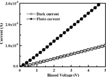
Figure 1 shows I-V characteristics of the fabricated ZnO MSM photoconductive sensor with Ni/Au electrodes, measured in dark 共dark current兲 and under illumination 共photocurrent兲. It can be seen that I-V characteristics of the fabricated sensors were symmetrical
z
E-mail: changsj@mail.ncku.edu.tw
Figure 1. I-V characteristics of the ZnO photoconductive sensor measured under dark and illumination.
Journal of The Electrochemical Society, 154共7兲 J209-J211 共2007兲
0013-4651/2007/154共7兲/J209/3/$20.00 © The Electrochemical Society J209
and linear. With 2 V applied bias, it was found that dark current and photocurrent of our ZnO MSM photoconductive sensor were 3.83 ⫻ 10−5and 1.21⫻ 10−4A, respectively. Figure 2 shows spectral
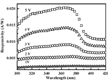
responses of the fabricated ZnO photoconductive sensors measured with various applied bias voltages. As shown in Fig. 2, it was found that measured sensor responsivities were almost independent of incident light wavelength within the wavelength range of 320–370 nm. As the incident light wavelength was further in-creased, it was found that the responsivity decreased rapidly due to the much smaller below bandgap absorption. On the other hand, it was found that the responsivity became smaller when the incident light wavelength was shorter than 320 nm. This is probably due to the fact that portion of the incident light was absorbed by the Ni/Au contact electrodes in the short wavelength region.23 It was also found that the peak responsivity increased almost linearly as we increased the applied bias voltage. With incident light wavelength of 370 nm and biased voltage of 5 V, it was found that measured re-sponsivity of the fabricated ZnO photoconductive sensor was 20.5 mA/W. Due to the large lattice mismatch between ZnO epitax-ial layer and sapphire substrate, it is known that threading disloca-tion in ZnO epitaxial layer is large in general. This large dislocadisloca-tion density often results in significant recombination of photogenerated carriers at sample surface and/or in the depletion region. Thus, we believe the relatively small 20.5 mA/W responsivity observed in this study is related to the high defect density in the epitaxial layer. Figure 3 shows measured noise spectra of the fabricated ZnO
photoconductive sensor. During noise measurements, we applied 0.5, 1, 2, 3, 4, and 5 V applied bias onto the sample. For compari-son, noise spectrum of a standard resistor was also shown in the same figure. It can be seen clearly that low-frequency noise of the standard resistor was almost independent of the frequency. In con-trast, the low-frequency noise spectra measured from the sensor could be fitted well by
Sn共f兲 = K
冉
IF
f␣
冊
关1兴where f is the frequency, Sn共 f兲 is the spectral density of noise power, K is a constant, IFis the dark current, and and ␣ are two fitting
parameters. As shown in Fig. 3, it was found that␣ equals unity when f⬍ 120 Hz. Such a result indicates that the low-frequency noise in the fabricated sensor was dominated by 1/f-type noise. Fig-ure 4 shows noise power density of our devices as a function of dark current measured at 10 Hz. It was found that was around 2. Such a value agrees well with Kleinpenning’s model that spectral density of the 1/f noise should proportional to IF2.24 We can also derive Hooge parameter of the fabricated sensors from the experimental data and25 SI共f兲 I2 = S共f兲 2 = S共f兲 2 = ␣H fN 关2兴
where, , ␣H, and N are the carrier mobility, conductivity of the
sample, Hooge parameter, and the total number of charge carriers, respectively. The value of N can be determined by
N = L
2
eR 关3兴
where L,, and R were electrode length, carrier mobility, and the resistance of the sample, respectively. From our experimental data, it was found that the total number of charge carriers共N兲 and the di-mensionless Hooge parameter共␣H兲 were 1.26 ⫻ 10−5cm−3and 2
⫻ 10−3, respectively. Previously, it has been reported that Hooge
parameter␣H of n-type GaN26and SiC27were both around 10−3.
These values are about the same as the Hooge parameter measured from our devices.
Note that noise power density was independent of frequency in the high-frequency region共i.e., above 120 Hz兲, as shown in Fig. 3. In the high-frequency region, shot noise will become dominant be-cause 1/f type noise will continue to decrease in this region. The total noise current power can be estimated by integrating Sn共 f兲 over the frequency range
Figure 2. Spectral responses of the fabricated ZnO photoconductive sensors measured with various applied bias voltages.
Figure 3. Measured noise spectra of the fabricated ZnO photoconductive sensor.
Figure 4. Noise power density of our devices as a function of dark current measured at 10 Hz.
J210 Journal of The Electrochemical Society, 154共7兲 J209-J211 共2007兲 J210
具in典2=
冕
0 B Sn共f兲df =冕
0 1 Sn共1兲df +冕
1 B Sn共f兲df = S0关ln共B兲 + 1兴 关4兴 Here, we assumed that Sn共 f兲 = Sn共1 Hz兲 when f ⬍ 1 Hz. Thus, the noise equivalent power共NEP兲 can be given byNEP =
冑
具in典2
R 关5兴
where R is the responsivity of the detector. The normalized detec-tivity共D*兲 can then be determined by
D*=
冑
A冑
BNEP 关6兴
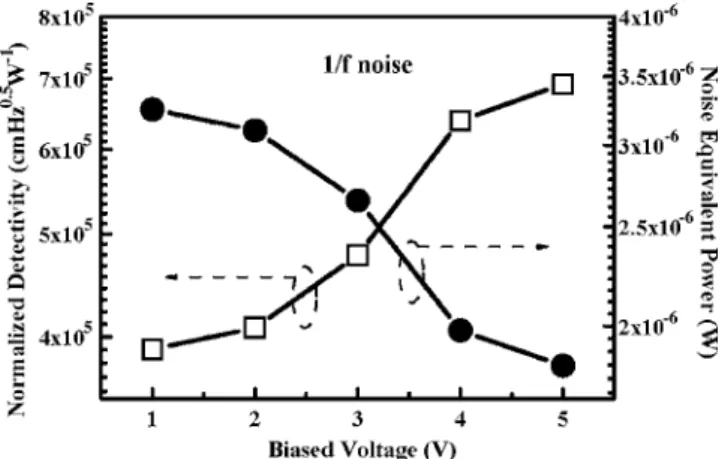
where A is the area of the detector and B is the bandwidth. For a given bandwidth of 1 kHz, we can thus determine noise equivalent power and detectivity as functions of applied voltage. As shown in Fig. 5, it was found that NEP decreased while D*increased
mono-tonically with the biased voltage. This is due to the fact that the increase in responsivity is much larger than the increase of total noise current power as the applied bias increased for the fabricated ZnO photoconductive sensor. Thus, NEP and D*of our
photocon-ductive sensor were both dominated by the total noise current power. With a 5 V applied bias, it was found that the NEP of 1.83⫻ 10−6W and the normalized detectivity of 6.91
⫻ 105cm Hz0.5W−1form our fabrication of ZnO photoconductive
sensors with Ni/Au electrodes. It is possible that the larger respon-sivity measured from our ZnO photoconductor sensor is attributed to the larger photocurrent gain. On the other hand, the extremely low normalized detectivity should be attributed to the high noise power.
Conclusions
In summary, epitaxial ZnO photoconductive sensors were fabri-cated on sapphire substrates. With an incident light wavelength of 370 nm and a 5 V applied bias, we achieved a sensor responsivity of 20.5 mA/W. With a 5 V applied bias, it was found that NEP and normalized detectivity of the fabricated sensors were 1.83 ⫻ 10−6W and 6.91⫻ 105cm Hz0.5W−1, respectively.
Acknowledgments
This work was supported by National Science Council under contract no. NSC 95-2221-E-006-314 and NSC 95-2221-E-006-357-MY3.
National Cheng Kung University assisted in meeting the publication costs of this article.
References
1. S. J. Chang, C. L. Yu, R. W. Chuang, P. C. Chang, Y. C. Lin, Y. W. Jhan, and C. H. Chen, IEEE Sens. J., 6, 1043共2006兲.
2. N. Vanhove, J. John, A. Lorenz, K. Cheng, G. Borghs, and J. E. M. Haverkort, Land Econ., 253, 2930共2006兲.
3. J. Ohsawa, T. Kozawa, O. Ishiguro, and H. Itho, Jpn. J. Appl. Phys., Part 1, 45, L435共2006兲.
4. T. K. Ko, S. J. Chang, Y. K. Su, Y. Z. Chiou, C. S. Chang, S. C. Shei, J. K. Sheu, W. C. Lai, Y. C. Lin, W. S. Chen, and C. F. Shen, IEEE Trans. Adv. Packag., 29, 483共2006兲.
5. T. K. Ko, S. J. Chang, J. K. Sheu, S. C. Shei, Y. Z. Chiou, M. L. Lee, C. F. Shen, S. P. Chang, and K. W. Lin, Semicond. Sci. Technol., 21, 1064共2006兲. 6. J. D. Hwang and C. C. Lin, Thin Solid Films, 491, 276共2005兲.
7. T. K. Lin, S. J. Chang, Y. Z. Chiou, C. K. Wang, S. P. Chang, K. T. Lam, Y. S. Sun, and B. R. Huang, Solid-State Electron., 50, 750共2006兲.
8. S. J. Chang, T. K. Lin, Y. K. Su, Y. Z. Chiou, C. K. Wang, S. P. Chang, C. M. Chang, J. J. Tang, and B. R. Huang, IEEE Sens. J., 6, 945共2006兲.
9. T. K. Lin, S. J. Chang, Y. K. Su, Y. Z. Chiou, C. K. Wang, C. M. Chang, and B. R. Huang, IEEE Trans. Electron Devices, 52, 121共2005兲.
10. T. K. Lin, S. J. Chang, Y. K. Su, Y. Z. Chiou, C. K. Wang, S. P. Chang, C. M. Chang, J. J. Tang, and B. R. Huang, Mater. Sci. Eng., B, 119, 202共2005兲. 11. S. J. Chang, T. K. Lin, Y. K. Su, Y. Z. Chiou, C. K. Wang, S. P. Chang, C. M.
Chang, J. J. Tang, and B. R. Huang, Mater. Sci. Eng., B, 127, 164共2006兲. 12. T. M. Barnes, J. Leaf, S. Hand, C. Fry, and C. A. Wolden, J. Appl. Phys., 96, 7036
共2004兲.
13. H. Kato, M. Sano, K. Miyanoto, and T. Yao, Jpn. J. Appl. Phys., Part 1, 42, L1002 共2003兲.
14. D. C. Look, Mater. Sci. Eng., B, 80, 383共2001兲.
15. Y. I. Alivov, E. V. Kalinina, A. E. Cherenkov, D. C. Look, B. M. Ataev, A. K. Omaev, M. V. Chukichev, and D. M. Bagnall, Appl. Phys. Lett., 83, 4719共2003兲. 16. N. R. Aghamalyan, R. K. Hovsepyan, A. R. Poghosyan, and V. G. Lazaryan, Proc.
SPIE, 5560, 235共2004兲.
17. S. Liang, H. Sheng, Y. Liu, Z. Huo, Y. Lu, and H. Shen, J. Cryst. Growth, 225, 110 共2001兲.
18. A. Mang, K. Reimann, and S. Rubenacke, Solid State Commun., 94, 251共1995兲. 19. H. Ohta, M. Kamiya, T. Kamiya, M. Hirano, and H. Hosono, Thin Solid Films,
445, 317共2003兲.
20. D. Basak, G. Amin, B. Mallik, G. K. Paul, and S. K. Sen, J. Cryst. Growth, 256, 73共2003兲.
21. C. L. Hsu, S. J. Chang, Y. R. Lin, P. C. Li, T. S. Lin, S. Y. Tsai, T. H. Lu, and I. C. Chen, Chem. Phys. Lett., 416, 75共2005兲.
22. M. Liu and H. K. Kim, Appl. Phys. Lett., 84, 173共2004兲.
23. T. K. Lin, S. J. Chang, B. R. Huang, K. T. Lam, Y. S. Sun, M. Fujita, and Y. Horikoshi, J. Electrochem. Soc., 153, G677共2006兲.
24. T. G. M. Kleinpenning, Solid-State Electron., 22, 121共1979兲. 25. F. N. Hooge, Physica (Amsterdam), 60, 130共1972兲.
26. S. L. Rumyantsev, N. Pala, M. S. Shur, R. Gaska, M. E. Levinshtein, M. A. Khan, G. Simin, X. Hu, and J. Yang, Electron. Lett., 37, 720共2001兲.
27. L. Anghel, T. Ouisse, T. Billon, P. Lassagne, and C. Jaussaud, Semicond. Int., 2, 539共1996兲.
Figure 5. Noise equivalent power and normalized detectivity of the 1/f type noise as functions of biased voltage.
J211 Journal of The Electrochemical Society, 154共7兲 J209-J211 共2007兲 J211