• 沒有找到結果。

Comparison of thermal stability and chemical bonding configurations of plasma oxynitrided Hf and Zr thin films

N/A
N/A
Protected

Academic year: 2022

Share "Comparison of thermal stability and chemical bonding configurations of plasma oxynitrided Hf and Zr thin films"

Copied!
7
0
0

加載中.... (立即查看全文)

全文

(1)

Comparison of Thermal Stability and Chemical Bonding Configurations of Plasma Oxynitrided Hf and Zr Thin Films

Yi-Sheng Lai, C. H. Lu, Li-Min Chen, and J. S. Chen * ,z

Department of Materials Science and Engineering, National Cheng Kung University, Tainan, Taiwan

In this work, we study the characteristics of plasma oxynitrided Hf and Zr thin films. A 5-nm-thick Hf or Zr metal film is deposited on the bare Si substrate, followed by plasma oxynitridation on these metal films in a N

2

O or NH

3

ambient. Incorporation of O and N leads to the formation of HfO

x

N

y

and ZrO

x

N

y

films. The high nitrogen content in the HfO

x

N

y

films prepared by NH

3

plasma oxynitridation is found to increase the onset of the crystallization temperature, as compared to films prepared by N

2

O plasma oxynitridation. Nevertheless, the difference in crystallization temperature is not seen for ZrO

x

N

y

films. The interlayer 共IL兲 between HfO

x

N

y

共or ZrO

x

N

y

兲 and Si is found to be thinner for the films with NH

3

plasma oxynitridation than those with N

2

O plasma oxynitridation. However, the nitrogen incorporated by plasma oxynitridation appears to be depleted after rapid thermal oxidation annealing and is not effective to inhibit the growth of the IL. The activation energy of the IL growth for N

2

O and NH

3

oxynitrided HfO

x

N

y

is 0.23 and 0.13 eV, respectively. The activation energy of the IL growth for N

2

O and NH

3

oxynitrided ZrO

x

N

y

is 0.19 and 0.14 eV, respectively.

© 2005 The Electrochemical Society. 关DOI: 10.1149/1.1993468兴 All rights reserved.

Manuscript submitted January 12, 2005; revised manuscript received April 25, 2005. Available electronically August 8, 2005.

Achieving high-performance complementary metal-oxide- semiconductor field-effect transistors drives the downscaling of sili- con technology forward. High dielectric constant 共␬兲 materials are becoming increasingly favorable due to the exponential increase in tunneling currents with decreasing SiO

2

thickness in the ultrathin regime. Of these, ZrO

2

and HfO

2

are the most promising candidates for their high relative dielectric constant 共␬ = 20-25兲 and good ther- mal stability. Applying high- ␬ materials can maintain the same gate capacitance in terms of the equivalent oxide thickness 共EOT兲 of SiO

2

while decreasing the tunneling current with a thicker physical thickness.

However, several issues associated with ZrO

2

and HfO

2

materi- als for gate-dielectric applications are encountered. For example, while they are thermodynamically stable in contact with Si, an in- terlayer 共IL兲 is still generated during the deposition and/or subse- quent post-annealing process.

1-3

It reveals that the degree of IL growth is highly dependent on the surface preparation, the deposi- tion, and the post-annealing conditions. Ferrari et al. have shown that short-time annealing is sufficient to form a relatively thick IL by means of injecting oxygen into Si from ZrO

2

and HfO

2

.

4

Therefore, it is suggested that oxide itself is also involved in the fast oxidation of Si at the initial stage. Thermal stability is a critical issue in re- placement of conventional SiO

2

gate dielectrics with high- ␬ materi- als. The IL growth as well as the interface reaction are of particular concern in this respect. Accordingly, engineering of the interface becomes a challenging issue in fabricating high- ␬ gate dielectrics.

Apart from the reduction of the gate dielectric thickness, it is feasible to reduce the EOT by means of reducing the thickness of the IL. Depositing the metal film followed by an oxidation process is a promising way to fabricate the gate dielectric with a low EOT.

Jeon et al. prepared ZrO

2

films by thermal oxidation of a sputter deposited Zr-metal layer and obtained encouraging results by opti- mizing the wet oxidation conditions.

5

Tsui et al. increased the Hf thickness and achieved a thinner IL in the HfO

2

/Hf stacks.

6

Yama- moto et al. made improvement in the electrical characteristics by blocking the oxygen from diffusing through the HfO

2

films into the Si substrates, due to oxidation of the Hf metal layer itself with an HfO

2

/Hf stacked structure.

7

As a consequence, the oxidation condi- tion appears to be the key factor determining the quality of the gate dielectric.

Nitrogen is considered to be the additive to stabilize the gate dielectrics either in high- ␬ materials or in the IL.

8,9

Many studies reported that nitrogen piled up at the interface will retard the growth

of SiO

2

.

10

Moreover, it also enhances resistance to boron diffusion,

11

increases time-dependent dielectric breakdown,

12

de- creases interface state density generation 共⌬D

it

兲 under electrical stress,

13

and suppresses hot carrier injection into the oxide.

14

How- ever, increasing the nitrogen content is far from being satisfactory, since it will increase the D

it

of as-grown films as well as worsen the reliability of negative-bias temperature instability.

15

Moreover, the incorporation of nitrogen at the oxide/semiconductor interface may degrade the channel mobility.

16

Therefore, it is important to control the nitrogen level in the film for reliable performance of the elec- tronic device.

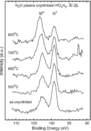
In this work, we investigate the characteristics of nominally 5-nm-thick Hf and Zr metal layers on Si followed by N

2

O or NH

3

plasma oxynitridation. The oxynitrided metal layers are then sub- jected to rapid thermal annealing at various temperatures. The IL growth and chemical bonding configurations of oxynitrided metal layers before and after rapid thermal annealing are discussed.

Experimental

The substrates used in this study were p-type mirror polished silicon 共100兲 wafers. The Si surface was cleaned by a modified Radio Corporation of America 共RCA兲 clean and then dipped in 1%

HF solution for 20 s to remove the chemical oxide, followed by a DI water rinse and N

2

dry.

The Hf and Zr metal layers were deposited by rf magnetron sputtering from the Hf target 共purity: 99.9%兲 and Zr target 共purity:

99.7% 兲, respectively. The chamber was pumped down to 4

⫻ 10

−6

Torr. Thicknesses of Hf and Zr metal layers were controlled to be nominally 5 nm. The Hf/Si or Zr/Si samples were then trans- ferred to another chamber for low-temperature plasma oxynitrida- tion. Plasma oxynitridation was carried out in a cold-wall, parallel- plate, plasma-enhanced chemical vapor deposition 共PECVD兲 chamber. Keeping the total pressure at 0.4 Torr and temperature at 450°C, capacitively coupled plasma was generated by a radio- frequency 共rf, 13.56 MHz兲 power supply connected to the shower- head plate with a power of 50 W and the substrate holder was grounded. The Hf/Si or Zr/Si samples were oxynitrided in N

2

O or NH

3

plasma for 150 s. NH

3

plasma also oxynitridized the films, where oxygen was unintentionally introduced because oxygen was always residual in the PECVD chamber. After oxynitridation, films were annealed in a Heatpulse 610i rapid thermal process chamber with flowing dry O

2

at temperatures ranging from 500 to 800°C for 30 s. The oxygen flow rate is 100 sccm and the oxygen pressure is 1 atm.

The phases of the structure were identified by a Rigaku D/MAX 2500 glancing incident angle X-ray diffraction 共GIAXRD兲 method with Cu K ␣ radiation at an incident angle of 2°. Chemical bonding

* Electrochemical Society Active Member.

z

E-mail: [email protected]

(2)

states of ultrathin HfO

x

N

y

/IL/Si and ZrO

x

N

y

/IL/Si structures were examined by using a VG ESCA-210 X-ray photoelectron spectro- scope 共XPS兲 equipped with a 12 kV Al/Mg X-ray source. XPS measurements were performed using Al K ␣ emission at 1486.6 eV.

Due to charge accumulation on the insulator surface, the spectra were corrected by shifting the peak of the Si 2p

3/2

to 99.0 eV.

17

The spin-orbit splitting of 0.6 eV and the area ratio of 1:2 are used for fitting the spectrum with the Si 2p

3/2

and 2p

1/2

peaks.

17

The background has been subtracted using a Shirley method. A method- ology to measure the SiO

2

IL thickness by XPS has been previously reported and a detailed description is given elsewhere.

18

Results and Discussion

Structure properties of HfO

x

N

y

and ZrO

x

N

y

films .— Figure 1a shows the GIAXRD patterns of N

2

O or NH

3

plasma oxynitrided HfO

x

N

y

films after rapid thermal oxidation 共RTO兲 annealing at 700 and 800°C. One can see that the 共111兲, 共220兲, and 共222兲 diffraction peaks of the tetragonal HfO

2

phase 共ICDD PDF 08-0342 兲

19

become pronounced for the N

2

O plasma oxynitrided sample after annealing at 700°C, but not for the NH

3

plasma oxynitrided sample. After annealing at 800°C, the diffraction patterns make no significant difference between the N

2

O and

NH

3

oxynitrided HfO

x

N

y

films. Our previous study on the plasma oxynitridation of Si reveals that, with the same treatment duration, more nitrogen atoms are incorporated in the films formed by NH

3

plasma oxynitridation than by N

2

O plasma oxynitridation.

20

A similar result is seen for the current study and will be shown later in Fig. 2. It suggests that the incorporation of nitrogen in the HfO

x

N

y

films may increase the crystallization temperature of HfO

2

. Lee et al. reported that incorporation of 4-11 atom % nitrogen in HfO

2

films increases the crystallization temperature from between 500 and 600°C to between 600 and 700°C.

21

In our case, the crystallization temperature for N

2

O and NH

3

oxynitrided HfO

x

N

y

films is between 600 and 700°C. It seems that the crystallization temperature for N

2

O oxynitrided HfO

x

N

y

films is lower than that for NH

3

oxynitrided HfO

x

N

y

films since the 共111兲 diffraction peak is more significant for N

2

O oxynitrided HfO

x

N

y

films. It does not show much difference in the crystallization temperature between N

2

O and NH

3

oxynitrided ZrO

x

N

y

films, as shown in Fig. 1b. The diffraction peaks are not conspicuous and are identified as 共111兲 and 共220兲 planes, which are associated with the tetragonal ZrO

2

phase 共ICDD PDF 17-0923兲. The intensity of the diffraction peak after annealing at 700°C 共not shown兲 is still the same as that after annealing at 600°C. We discuss the different behavior in the crystallization temperature between ZrO

x

N

y

films and HfO

x

N

y

films in the next section.

Chemical bonding configurations of HfO

x

N

y

and ZrO

x

N

y

films .— Figure 2a and b shows XPS spectra of N 1s core levels of Hf and Zr thin films after N

2

O and NH

3

plasma oxynitridation. It shows that the integrated intensity for the spectra of the NH

3

plasma Figure 1. GIAXRD patterns of 共a兲 HfO

x

N

y

films after RTO annealing at

700 and 800°C, and 共b兲 ZrO

x

N

y

films after RTO annealing at 500 and 600°C.

The XRD pattern of as-sputtered Hf and Zr films 共without plasma treatment兲 are also shown for reference.

Figure 2. XPS spectra of N 1s core levels of 共a兲 Hf and 共b兲 Zr thin films

after N

2

O or NH

3

plasma oxynitridation. It is shown that NH

3

plasma

oxynitrided samples exhibit a greater integrated area than N

2

O plasma

oxynitrided ones.

(3)

oxynitrided samples is greater than that for N

2

O oxynitrided samples. As a result, the NH

3

plasma oxynitridation process incor- porates more nitrogen in the HfO

x

N

y

/IL/Si and ZrO

x

N

y

/IL/Si stacks than the N

2

O plasma oxynitridation process does. For HfO

x

N

y

films, the N 1s spectra show a broad peak which is composed of several bonding states, i.e., the N atom bonds to Hf atoms or O atoms. The binding energy 共BE兲 for N⬅Hf

3

varies from 396.0 to 396.9 eV, depending on the N content and deposition conditions.

22

Typically, one N atom can bond to three atoms. The electronegativity for Hf, N, and O is 1.3, 3.04, and 3.44, respectively.

23

The BE of the nitro- gen 1s core levels will be the lowest if the N atom bonds to three Hf atoms. Conversely, when Hf atoms in the N ⬅Hf

3

bonding configu- ration are substituted with O atoms, the BE will shift to a higher value. To the best of our knowledge, we have not found reported BE data of nitrogen 1s core levels in Hf

2

=N-O and Hf-N=O

2

bondings.

However, Rignanese et al. demonstrated that the BE of Si

2

=N-O and Si

2

-N=O

2

are 401.3 and 403.6 eV.

24

Because the electronegativity of Si 共1.90兲 is greater than that of Hf, the BEs are expected to be lower than 401.3 and 403.6 eV for Hf

2

=N-O and Hf-N=O

2

. Because the incorporated nitrogen is possibly embedded in both the hafnium-rich and oxygen-rich regions, the observed BE of N 1s core levels in HfO

x

N

y

films ranges from ⬃396 to ⬃403 eV, suggestive of a wide peak in Fig. 2a and b.

As for ZrO

x

N

y

films, the peaks of N 1s core levels at 399.9 ± 0.3 eV and 397.7 ± 0.2 eV are observed for samples pre- pared by N

2

O plasma oxynitridation and NH

3

plasma oxynitrida- tion, respectively. Prieto et al. demonstrated that the BE of N ⬅Zr

3

is 397.3 eV.

25

Accordingly, the main bonding configuration for NH

3

plasma oxynitrided ZrO

x

N

y

films is supposed to be N ⬅Zr

3

. How- ever, the BE of the N ⬅Zr

3

in our sample shows a higher value than the reported one, which may arise from the second-nearest-neighbor effect. That is, the O atom, which bonds to the Zr atom as the nearest neighbor, in the ZrO

x

N

y

films 共e.g., Zr-O

N

4-␦

, ␦ = 1, 2, 3兲 will shift the N 1s peak to a higher BE. The degree of the shift is dependent on the oxygen content. As a consequence, the BE is ob- served to be larger than 397.3 eV. The BE of the N 1s peak for the N

2

O plasma oxynitrided film is higher than that of the NH

3

plasma oxynitrided one by about 2 eV. It suggests that the N atom may directly bond to one oxygen atom 共i.e., Zr

2

v N-O兲 in the N

2

O plasma oxynitrided ZrO

x

N

y

films.

Plasma oxynitridation is supposed to introduce more nitrogen at the surface and therefore the depth profile of nitrogen may not be uniform in our case. This makes it difficult to determine the real nitrogen content of the HfO

x

N

y

and ZrO

x

N

y

films. Considering that the depth distribution of nitrogen in HfO

x

N

y

and ZrO

x

N

y

films is uniform, we integrate the intensity area of Hf 4f, Zr 3d, O 1s 共O in the IL is not included 兲, and N 1s spectra, and the areas are divided by their sensitivity factors, respectively. The 关N兴 levels for N

2

O and

NH

3

oxynitrided HfO

x

N

y

films are 4.9 and 7.8%, respectively. The 关N兴 levels for N

2

O and NH

3

oxynitrided ZrO

x

N

y

films are 3.1 and 5.9%, respectively.

HfO

2

and ZrO

2

are expected to behave similarly and they are elements of group IV B in the periodic table. However, in our case, the N 1s spectra show the difference between plasma oxynitridized HfO

x

N

y

and ZrO

x

N

y

films. The nitrogen content of HfO

x

N

y

films is also shown to be higher than that of ZrO

x

N

y

films.

Besides, the HfO

x

N

y

films contain more unstable N-O and N-O

2

bondings than ZrO

x

N

y

films. The lattice constants for tetragonal HfO

2

共a = 5.15 Å, c = 5.29 Å兲 are reported to be larger than the tetragonal ZrO

2

共a = 5.05 Å, c = 5.18 Å兲.

26

The atomic radii are nearly the same for Hf 共1.56 Å兲 and Zr 共1.59 Å兲, but the smaller volume density of HfO

2

may be more suitable for nitrogen 共atomic radius = 0.55 Å 兲 incorporation via plasma treatments.

After RTO annealing at 500°C, both HfO

x

N

y

and ZrO

x

N

y

films reveal their N 1s spectra with no significant peak 共not shown兲. The disappearance of the N 1s signal may be attributed to the following two reasons. First, the incorporated nitrogen is unstable within the HfO

x

N

y

and ZrO

x

N

y

films. Kim et al. showed that the nitrogen species formed by energetic plasma process is kinetically trapped within the shallow part of the film.

27

The bonding state of nitrogen is likely to be thermally unstable. Miotti et al. demonstrated that the near-surface nitrogen is lost in exchange for O when annealing in oxygen ambient.

28

Hence, the nitrogen is depleted after RTO anneal- ing. Second, the N 1s signal does not disappear because N atoms tend to pile up at the IL/Si interface upon annealing, at which the photoelectron signal decays exponentially with the depth. Therefore, it is hard to detect the N 1s signal. In summary, we propose that part of the nitrogen in the films is dissociated into the air and the other part of the nitrogen is driven to the IL/Si interface during RTO annealing.

NH

3

plasma oxynitridation is shown to incorporate more nitro- gen in the films. Therefore, the crystallization of NH

3

plasma ox- ynitrided HfO

x

N

y

films needs to be conducted at a higher tempera- ture, as compared to N

2

O plasma oxynitrided HfO

x

N

y

films, to deplete nitrogen atoms first and then crystallize the HfO

2

. As a result, the crystallization temperature is higher for the NH

3

plasma oxynitrided HfO

x

N

y

, as shown in Fig. 1a. However, the rich-N content in NH

3

plasma oxynitrided ZrO

x

N

y

does not defer its crystallization from our results. It is proposed that the thermal bud- get for the nitrogen depletion in ZrO

x

N

y

films is lower than that of HfO

x

N

y

films. Consequently, the crystallization temperature of ZrO

x

N

y

films does not show much difference via N

2

O or NH

3

plasma oxynitridation.

Table I lists the BEs and full widths at half maximum 共fwhms兲 of Hf 4f

7/2

, O 1s, and Si

4+

2p core-level electrons for Hf films Table I. Binding energies and fwhms of Hf 4f

7/2

, O 1s, and Si

4+

2p core-level electrons for Hf films after N

2

O or NH

3

plasma oxynitridation. The films are then subjected to RTO annealing at 500, 600, 700, and 800°C for 30 s. The spin-orbit splitting of 1.71 eV and the area ratio of 4:3 between the Hf 4f

7/2

and 4f

5/2

were applied for fitting the spectra. The O 1s photoelectron peak is deconvoluted into two components repre- senting the signals from the HfO

x

N

y

and the IL, respectively.

System Condition

Hf 4f

7/2

BE/fwhm

共eV兲

O 1s BE/fwhm

共eV兲

O 1s 共IL兲 BE/fwhm 共eV兲

Si

4+

2p BE/fwhm

共eV兲

N

2

O plasma oxynitrided Hf/Si As 17.3/1.61 530.8/1.88 532.3/2.02 102.5/1.95

500°C 30 s 17.4/1.59 530.9/1.88 532.4/2.02 102.5/1.93

600°C 30 s 17.3/1.54 530.8/1.88 532.2/2.02 102.4/1.90

700°C 30 s 17.6/1.56 531.2/1.88 532.8/2.02 103.0/1.92

800°C 30 s 18.0/1.52 531.5/1.88 533.0/2.02 103.3/1.89

NH

3

plasma oxynitrided Hf/Si As 17.4/1.58 530.8/1.88 532.3/2.02 102.2/1.93

500°C 30 s 17.3/1.56 530.7/1.88 532.2/2.02 102.3/1.90

600°C 30 s 17.2/1.59 530.7/1.89 532.1/2.02 102.4/1.93

700°C 30 s 17.5/1.61 531.0/1.88 532.4/2.02 102.8/1.96

800°C 30 s 18.0/1.52 531.5/1.88 533.0/2.02 103.3/1.88

(4)

prepared by N

2

O or NH

3

plasma oxynitridation, followed by RTO annealing at 500, 600, 700, and 800°C for 30 s. The spin-orbit splitting of 1.71 eV and the area ratio of 4:3 between the Hf 4f

7/2

and 4f

5/2

were applied for fitting the Hf 4f spectra, as shown in Fig.

3a.

29

The BEs of the Hf 4f

7/2

core level for N

2

O and NH

3

oxyni- trided HfO

x

N

y

are 17.3 and 17.4 eV, respectively. The reported BE of the Hf 4f

7/2

core level for HfN ranges from 15.0 to 15.5 eV, depending on the nitrogen content of the film, while that for HfO

2

is 17.9 eV.

30

No peak pertaining to metallic Hf is found in the Hf 4f spectra. It suggests that plasma oxynitridation process is efficient to transform the ultrathin metallic Hf films into HfO

x

N

y

films. Anneal-

ing the as-oxynitrided HfO

x

N

y

films to 800°C results in a 0.6 and 0.7 eV BE shift of Hf 4f

7/2

core levels for N

2

O plasma oxynitrided and NH

3

plasma oxynitrided samples, respectively. The value is near the BE of Hf4f

7/2

core levels for HfO

2

films reported in the literature.

30

Table II shows the BEs and fwhms of Zr 3d

5/2

, O 1s, and Si

4+

2p core-level electrons for Zr films after N

2

O or NH

3

plasma oxynitri- dation, followed by RTO annealing at 500, 600, and 700°C for 30 s.

The spin-orbit splitting of 2.43 eV and the area ratio of 3:2 between the Zr 3d

5/2

and 3d

3/2

were applied for fitting the Zr 3d spectra, as shown in Fig. 3b.

29

The BEs of Zr 3d

5/2

core levels for N

2

O and NH

3

oxynitrided ZrO

x

N

y

are 182.5 and 182.2 eV, respectively. The reported BEs of Zr 3d

5/2

core levels for metallic Zr and ZrO

2

from the literature are 178.7 and 183.3 eV, respectively.

31,32

The BEs of Zr 3d

5/2

core levels for ZrN

x

共x = 0.7-1.0兲 and Zr

3

N

4

are 0.6–1.3 eV and 2.0 eV higher than that of metallic Zr, respectively.

25

An- nealing the as-oxynitrided ZrO

x

N

y

films to 700°C leads to a 0.7 and 0.8 eV BE shift of Zr 3d

5/2

core levels for N

2

O plasma oxynitrida- tion and NH

3

plasma oxynitridation, respectively, as given in Table II. The value is near the BE of Zr 3d

5/2

core levels for ZrO

2

films in the literature.

31,32

The O 1s peak is composed of signals from the HfO

x

N

y

or ZrO

x

N

y

films and the IL. Hence, to understand the bonding configu- ration before and after RTO annealing, a deconvolution process is conducted to resolve the two peaks. The O 1s spectrum is deconvo- luted on the basis of their asymmetric shape. The fwhm of O-Hf and O-Zr is determined by fitting thick HfO

2

and ZrO

2

films deposited on a Si substrate. The BE of the O 1s 共IL兲 peak is determined from the shoulder position. The deconvoluted peaks with their BEs and fwhms are summarized in Tables I and II. It is suggested that the intensity of the O 1s peaks from the high- ␬ film and the IL shifts to high BEs after RTO annealing, indicative of the increased oxygen content in the stacks.

Comparing the two tables, one can see that the BEs of Hf 4f, Zr 3d, O 1s, and Si

4+

2p core levels are all shifted to higher values after RTO annealing. It is assumed that the plasma oxynitridation process is not sufficient to supply enough oxygen or nitrogen into the HfO

x

N

y

or the ZrO

x

N

y

films, so the oxygen and nitrogen in the films are possibly understoichiometry 共x + y ⬍ 2兲. In addition, even though the N 1s spectra of as-oxynitrided samples are different for N

2

O and NH

3

plasma processes 共i.e., the nitrogen content and bond- ing configurations 兲, oxygen atoms which are incorporated into the films during the RTO annealing may deplete the nitrogen, regardless of the initial nitrogen concentration. Owing to its high electronega- tivity, the increased oxygen content in the films subsequently in- creases the BEs of the core-level electrons of all elements. The two tables also show the increase in Si

4+

as a function of RTO annealing temperatures. In HfO

x

N

y

and ZrO

x

N

y

cases, the BE of Si

4+

via N

2

O

Table II. Binding energies and fwhms of Zr 3d

5/2

, O 1s, and Si

4+

2p core-level electrons for Zr films after N

2

O or NH

3

plasma oxynitridation.

The films are then subjected to RTO annealing at 500, 600, and 700°C for 30 s. The spin-orbit splitting of 2.43 eV and the area ratio of 3:2 between the Zr 3d

5/2

and 3d

3/2

applied for fitting the spectra. The O 1s photoelectron peak is deconvoluted into two components representing the signals from the ZrO

x

N

y

and the IL, respectively.

System Condition

Zr 3d

5/2

BE/fwhm

共eV兲

O 1s BE/fwhm

共eV兲

O 1s 共IL兲 BE/fwhm

共eV兲

Si

4+

2p BE/fwhm

共eV兲

N

2

O plasma oxynitrided Zr/Si As 182.5/1.68 530.5/1.88 532.3/2.01 102.6/2.07

500°C 30 s 182.7/1.67 530.7/1.89 532.4/2.01 102.7/2.04

600°C 30 s 183.1/1.58 531.0/1.88 532.7/2.02 103.0/1.98

700°C 30 s 183.2/1.59 531.2/1.88 532.9/2.02 103.3/2.01

NH

3

plasma oxynitrided Zr/Si As 182.2/1.65 530.2/1.88 531.9/2.02 101.8/2.02

500°C 30 s 182.4/1.62 530.3/1.88 532.1/2.02 102.3/1.99

600°C 30 s 182.7/1.62 530.7/1.88 532.5/2.02 102.6/1.95

700°C 30 s 183.0/1.56 531.1/1.88 532.6/2.02 102.9/2.02

Figure 3. XPS spectra of 共a兲 Hf 4f core levels of HfO

x

N

y

films and 共b兲 Zr 3d

core levels of ZrO

x

N

y

films after N

2

O or NH

3

plasma oxynitridation.

(5)

plasma oxynitridation is higher than that via NH

3

plasma oxynitri- dation. The BE difference may be due to different IL thicknesses

33

and nitrogen contents.

A snap back of BEs of Hf 4f core levels is observed in both the N

2

O and NH

3

cases after RTO annealing. It may be relevant to the initial state of as-oxynitridized HfO

x

N

y

. As is shown in the N 1s spectra of HfO

x

N

y

and ZrO

x

N

y

, the HfO

x

N

y

film contains more N-O and N-O

2

states than ZrO

x

N

y

does. After RTO annealing at 500 and 600°C, the nitrogen depletes while the supply of oxygen for HfO

x

N

y

films is not as much as the as-oxynitrided films. The as- oxynitridized HfO

x

N

y

structure shall be relaxed after annealing at 500 and 600°C. In other words, the plasma process incorporates more N and O in the vicinity of Hf for as-oxynitrided HfO

x

N

y

films as compared to the N and O content of the HfO

x

N

y

films annealed at 500 and 600°C.

Interlayer growth behavior. .— Figure 4a and b shows the XPS spectra of Si 2p core levels of Hf and Zr thin films after N

2

O or NH

3

plasma oxynitridation. The Si

4+

peak is associated with the Si tetra- hedral bondings 共to four foreign atoms兲 in the IL, and the Si

0

2p

3/2

and 2p

1/2

peaks arise from the pure Si networks of the Si substrate.

A peak representative of the interface states 共Si

1+

, Si

2+

, and Si

3+

兲 is also fitted in the Si 2p spectra. The number of escaped photoelec- trons without losing their energy decays exponentially as 共−d/␭兲 with its depth d from surface, where ␭ is the inelastic mean free path of a photoelectron. The intensity of Si

0

depends inversely on the total thickness of HfO

x

N

y

/IL or ZrO

x

N

y

/IL film stacks, whereas that of Si

4+

increases with the increasing thickness of IL. The IL may be SiO

2

or a metal silicate layer. It is found that the IL is thicker for the samples prepared by N

2

O plasma oxynitridation than by NH

3

plasma oxynitridation. This observation is conceivable since N

2

O may dissociate into both oxidizing and nitridizing species

34

whereas NH

3

produces nitridizing species only.

35

The oxidizing species will react with the Si substrate and assist the growth of the IL. However, the nitridizing species will introduce nitrogen at the interface and retard the growth of the IL, leading to a thinner IL.

Figure 5 shows XPS spectra of Si 2p core levels on the surface of N

2

O plasma oxynitrided HfO

x

N

y

films on Si, before and after RTO annealing at 500-800°C for 30 s. It is observed that the Si

4+

peak increases whereas the Si

0

peak attenuates with annealing tem- peratures. It is conceivable that the IL grows when annealed in oxy- gen ambient and the IL thickness increases with the increasing an- nealing temperature. The IL growth upon RTO annealing in the ZrO

x

N

y

system shows a similar trend and thus the spectra are not shown here.

Figure 6a and b shows the IL thickness obtained from the Si 2p spectra. The method of extracting the IL thickness is described in Ref. 18. Though the initial IL thickness is thinner for NH

3

plasma oxynitrided films, it is observed that the IL of the samples prepared by NH

3

plasma oxynitridation grows faster than those by N

2

O plasma oxynitridation after RTO annealing. The IL thicknesses are nearly the same for N

2

O and NH

3

plasma oxynitrided HfO

x

N

y

after RTO annealing, whereas the IL grows slower for N

2

O plasma ox- ynitrided ZrO

x

N

y

than for NH

3

plasma oxynitrided ZrO

x

N

y

. The IL growth rate is observed to be higher for NH

3

oxynitrided films than N

2

O treated ones even though NH

3

plasma oxynitrided HfO

x

N

y

and ZrO

x

N

y

contain more nitrogen. The phenomena may be related to the hydrogen effect. Hydrogen is the species which is often intro- duced via NH

3

plasma process and it may play an important role in the assistance of the IL growth. H

2

O molecules and hydroxyl groups are known to be efficient oxidants. The hydrogen atoms exist in the IL/Si interface of NH

3

plasma. Oxynitrided samples may form the hydroxyl group that will attack the Si-Si backbond, and in turn, the IL growth rate thus increases.

36

The growth rate for NH

3

plasma oxynitrided samples 共HfO

x

N

y

or ZrO

x

N

y

兲 is higher than the N

2

O plasma oxynitrided one. After an- nealing at 700°C, the IL thicknesses for N

2

O- and NH

3

-treated

HfO

x

N

y

films and NH

3

-treated ZrO

x

N

y

films are all around 27-28 Å, while that for the N

2

O-treated ZrO

x

N

y

films is around 23-24 Å.

There are three factors that will affect the IL growth: 共i兲 the nitrogen

in the films and at the IL/Si interface, 共ii兲 the oxygen diffusivity

through the nitrided films, and 共iii兲 the hydrogen effect. The IL

growth rate is observed to be lower in N

2

O plasma oxynitrided

ZrO

x

N

y

films, and we think that it may be due to nitrogen piled up

at the IL/Si interface to retard the IL growth and no hydrogen to

assist the growth of the IL with the N

2

O plasma treatment. However,

the retardation of the IL growth is not seen for HfO

x

N

y

films with

the N

2

O plasma treatment. It may be ascribed to the lower crystal-

lization temperature 共⬍700°C兲 of HfO

x

N

y

films with the N

2

O

plasma treatment than that with NH

3

plasma treatment, as shown in

Figure 4. XPS spectra of Si 2p core levels of 共a兲 Hf and 共b兲 Zr thin films

after N

2

O or NH

3

plasma oxynitridation. The Si

4+

peak is associated with the

Si tetrahedral bondings 共to four foreign atoms兲 in the IL and the Si

0

2p

3/2

and

Si

0

2p

1/2

peaks arise from the pure Si networks of the Si substrate. The

positions of the decomposed 2p

3/2

and 2p

1/2

peaks were 99.0 and 99.6 eV,

respectively.

(6)

Fig. 1a. The grain boundary may enhance the oxygen diffusivity and consequently increase the IL thickness.

Figure 7a and b shows the Arrhenius plot of the IL growth in the N

2

O and NH

3

plasma oxynitrided HfO

x

N

y

and ZrO

x

N

y

, respec- tively. The IL growth rate is found to be governed by the Arrhenius law

d − d

0

t = A exp

− E KT

a

where E

a

and A are the activation energy and preexponential factor for a reaction process. d

0

is the initial thickness of as-oxynitrided IL, and d is the IL thickness after RTO annealing for duration t, at a given temperature T. The activation energy for the IL growth of N

2

O and NH

3

plasma oxynitrided HfO

x

N

y

is 0.23 and 0.13 eV, respectively. It is found that the activation energy of N

2

O oxyni- trided HfO

x

N

y

is higher than that of NH

3

oxynitrided HfO

x

N

y

. The difference in the activation energy of the IL growth between N

2

O and NH

3

plasma oxynitrided samples is possibly due to the greater initial thickness of the IL in the N

2

O plasma oxynitrided samples.

The value is comparable to the activation energy of 0.25 eV for the IL growth of HfO

x

N

y

films containing 4 atom % N, as demonstrated by Lee et al.

21

Moreover, the activation energy for the IL growth of N

2

O and NH

3

oxynitrided ZrO

x

N

y

is 0.19 and 0.14 eV, respectively.

It is also shown that the activation energy of N

2

O oxynitrided ZrO

x

N

y

is higher than that of NH

3

oxynitrided ZrO

x

N

y

, which is in accordance with the result of the HfO

x

N

y

system.

Conclusions

In this work, we study the characteristics of N

2

O and NH

3

plasma oxynitrided HfO

x

N

y

and ZrO

x

N

y

films. It is revealed that NH

3

plasma oxynitrided HfO

x

N

y

and ZrO

x

N

y

films exhibit a thinner Figure 5. XPS spectra of Si 2p core levels on the surface of N

2

O plasma

oxynitrided HfO

x

N

y

films on Si, before and after RTO annealing at 500-800°C for 30 s.

Figure 6. IL thickness for N

2

O and NH

3

plasma oxynitrided 共a兲 Hf/Si and 共b兲 Zr/Si systems as a function of RTO annealing at various temperatures.

The IL thickness is extracted from Si 2p spectra.

Figure 7. Arrhenius plots of the IL growth in the N

2

O and NH

3

plasma

oxynitrided 共a兲 HfO

x

N

y

and 共b兲 ZrO

x

N

y

films.

(7)

interlayer 共IL兲 than N

2

O plasma oxynitrided ones. In addition, NH

3

plasma oxynitridation incorporates more nitrogen on the HfO

x

N

y

/IL and ZrO

x

N

y

/IL film stacks. However, the nitrogen is depleted and the IL grows thicker upon RTO annealing. The activation energy of the IL growth is higher for N

2

O plasma oxynitrided samples than for NH

3

plasma oxynitrided ones, which may be attributed to the greater initial IL thickness in the N

2

O plasma oxynitrided samples.

Plasma oxynitridation is an effective method to fabricate HfO

x

N

y

and ZrO

x

N

y

films at low temperature as compared to rapid thermal nitridation for ULSI technology.

Acknowledgments

The authors gratefully thank R.-C. Li for his support with the XPS instrument and they appreciate the financial support from the National Science Council of Taiwan, ROC and Applied Materials Taiwan 共grant no. NSC 92-2623-7-006-015 and NSC 94-2623-7- 006-020-AT 兲.

National Cheng Kung University assisted in meeting the publication costs of this article.

References

1. M. Kundu, N. Miyata, and M. Ichikawa, J. Appl. Phys., 93, 1498 共2003兲.

2. Y.-S. Lin, R. Puthenkovilakam, J. P. Chang, C. Bouldin, I. Levin, N. V. Nguyen, J. Ehrstein, Y. Sun, P. Pianetta, T. Conard, W. Vandervorst, V. Venturo, and S. Selbrede, J. Appl. Phys., 93, 5945 共2003兲.

3. K.-J. Choi, J.-B. Park, and S.-G. Yoon, J. Electrochem. Soc., 150, F75 共2003兲.

4. S. Ferrari and G. Scarel, J. Appl. Phys., 96, 144 共2004兲.

5. S. Jeon and H. Hwang, J. Vac. Sci. Technol. B, 20, 400 共2002兲.

6. B.-Y. Tsui and H.-W. Chang, J. Appl. Phys., 93, 10119 共2003兲.

7. K. Yamamoto, S. Hayashi, M. Kubota, and M. Niwa, Appl. Phys. Lett., 81, 2053 共2002兲.

8. C. S. Kang, H.-J. Cho, K. Onishi, R. Nieh, R. Choi, S. Gopalan, S. Krishnan, J. H.

Han, and J. C. Lee, Appl. Phys. Lett., 81, 2593 共2002兲.

9. P. D. Kirsch, C. S. Kang, J. Lozano, J. C. Lee, and J. G. Ekerdt, J. Appl. Phys., 91, 4353 共2002兲.

10. M. L. Green, E. P. Gusev, R. Degraeve, and E. L. Garfunkel, J. Appl. Phys., 90, 2057 共2001兲.

11. C. T. Liu, Y. Ma, H. Luftman, and S. J. Hillenius, IEEE Electron Device Lett., 18, 212 共1997兲.

12. M. Beichele, A. J. Bauer, M. Herden, and H. Ryssel, Solid-State Electron., 45, 1383 共2001兲.

13. M. Bhat, J. Kim, J. Yan, G. W. Yoon, L. K. Han, and D. L. Kwong, IEEE Electron Device Lett., 15, 421 共1994兲.

14. H. Huang, W. Ting, D.-L. Kwong, and J. Lee, IEEE Electron Device Lett., 12, 495 共1991兲.

15. D. K. Schroder and J. A. Babcock, J. Appl. Phys., 94, 1 共2003兲.

16. C. Y. Kang, H.-J. Cho, R. Choi, C. S. Kang, Y. H. Kim, S. J. Rhee, C. H. Choi, S.

M. Akbar, and J. C. Lee, Appl. Phys. Lett., 84, 2148 共2004兲.

17. J. Himpsel, F. R. McFeely, A. Taleb-Ibrahimi, J. A. Yarmoff, and G. Hollinger, Phys. Rev. B, 38, 6084 共1988兲.

18. Y.-S. Lai, J. S. Chen, and J. L. Wang, J. Electrochem. Soc., 151, F135 共2004兲.

19. International Centre for Diffraction Data - Powder Diffraction File.

20. Y.-S. Lai and J. S. Chen, J. Vac. Sci. Technol. A, 21, 772 共2003兲.

21. M. Lee, Z.-H. Lu, W.-T. Ng, D. Landheer, X. Wu, and S. Moisa, Appl. Phys. Lett., 83, 2638 共2003兲.

22. A. Arranz, Surf. Sci., 563, 1 共2004兲.

23. CRC Handbook of Chemistry and Physics, 83th ed., D. R. Lide, Editor, CRC Press, Boca Raton, FL 共2003兲.

24. G.-M. Rignanese and A. Pasquarello, Phys. Rev. B, 63, 075307 共2001兲.

25. P. Prieto, L. Galán, and J. M. Sanz, Phys. Rev. B, 47, 1613 共1993兲.

26. G.-M. Rignanese, X. Gonze, G. Jun, K. Cho, and A. Pasquarello, Phys. Rev. B, 69, 184301 共2004兲

27. Y. K. Kim, H. S. Lee, H. W. Yeom, D.-Y. Ryoo, S.-B. Huh, and J.-G. Lee, Phys.

Rev. B, 70, 165320 共2004兲.

28. L. Miotti, K. P. Bastos, G. V. Soares, C. Driemeier, R. P. Pezzi, J. Morais, I. J. R.

Baumvol, A. L. P. Rotondaro, M. R. Visokay, J. J. Chambers, M. Quevedo-Lopez, and L. Colombo, Appl. Phys. Lett., 85, 4460 共2004兲.

29. J. F. Moulder, W. F. Stickle, P. E. Sobol, and K. D. Bomben, Handbook of X-Ray Photoelectron Spectroscopy, J. Chastain and R. C. King, Jr., Editors, Physical Elec- tronics Inc., Eden Prairie, MN 共1995兲.

30. C. Morant, L. Galan, and J. M. Sanz, Surf. Interface Anal., 16, 304 共1990兲.

31. A. Lyapin, L. P. H. Jeurgens, P. C. J. Graat, and E. J. Mittemeijer, J. Appl. Phys., 96, 7126 共2004兲.

32. R. Kaufmann, H. Klewe-Nebenius, H. Moers, G. Pfennig, H. Jenett, and H. Ache, Surf. Interface Anal., 11, 502 共1988兲.

33. A. Pasquarello, M. S. Hybertsen, and R. Car, Phys. Rev. B, 53, 10942 共1996兲.

34. K. A. Ellis and R. A. Buhrman, IBM J. Res. Dev., 43, 287 共1999兲.

35. X. Xu, S.-Y. Kang, and T. Yamabe, Chem.-Eur. J., 8, 5351 共2002兲.

36. F.-M. Liu, B. Ren, J.-W. Yan, B.-W. Mao, and Z.-Q. Tian, J. Electrochem. Soc.,

149, G95 共2002兲.

數據

Figure 2. XPS spectra of N 1s core levels of 共a兲 Hf and 共b兲 Zr thin films after N 2 O or NH 3 plasma oxynitridation
Table I lists the BEs and full widths at half maximum 共fwhms兲 of Hf 4f 7/2 , O 1s, and Si 4+ 2p core-level electrons for Hf filmsTable I
Table II shows the BEs and fwhms of Zr 3d 5/2 , O 1s, and Si 4+ 2p core-level electrons for Zr films after N 2 O or NH 3 plasma  oxynitri-dation, followed by RTO annealing at 500, 600, and 700°C for 30 s.
Figure 5 shows XPS spectra of Si 2p core levels on the surface of N 2 O plasma oxynitrided HfO x N y films on Si, before and after RTO annealing at 500-800°C for 30 s
+2

參考文獻

相關文件

We do it by reducing the first order system to a vectorial Schr¨ odinger type equation containing conductivity coefficient in matrix potential coefficient as in [3], [13] and use

The existence and the uniqueness of the same ratio points for given n and k.. The properties about geometric measurement for given n

• To enhance teachers’ knowledge and understanding about the learning and teaching of grammar in context through the use of various e-learning resources in the primary

220V 50 Hz single phase A.C., variable stroke control, electrical components and cabling conformed to the latest B.S.S., earthing through 3 core supply cable.. and 2,300 r.p.m.,

Wang, Solving pseudomonotone variational inequalities and pseudocon- vex optimization problems using the projection neural network, IEEE Transactions on Neural Networks 17

Define instead the imaginary.. potential, magnetic field, lattice…) Dirac-BdG Hamiltonian:. with small, and matrix

S1 Singlet-triplet energy gap (in kcal/mol) of n-cyclacene as a function of the number of benzene rings, calculated using TAO-LDA and KS-LDA.. For com- parison, the CASPT2, KS-M06L,

Consistent with the negative price of systematic volatility risk found by the option pricing studies, we see lower average raw returns, CAPM alphas, and FF-3 alphas with higher