行政院國家科學委員會專題研究計畫 期中進度報告
利用耦合線、非均勻傳輸線及 Z 轉換技術設計製作多頻帶濾 波器(1/2)
計畫類別: 個別型計畫
計畫編號: NSC91-2213-E-011-075-
執行期間: 91 年 08 月 01 日至 92 年 07 月 31 日 執行單位: 國立臺灣科技大學電子工程系
計畫主持人: 徐敬文
計畫參與人員: 陳凰美 蘇家信 陳鼎凱 劉俊麟 甘世宗 李仲桓
報告類型: 精簡報告
處理方式: 本計畫可公開查詢
中 華 民 國 92 年 6 月 3 日
期中報告
利用耦合線、非均勻傳輸線及 Z 轉換技術設計製作多頻帶濾波器 A Study on multiband filter s using nonunifor m/coupled lines and
Z-tr ansfor m technique
計劃編號:NSC 91-2213-E-011 –075 – 計劃主持人:徐敬文
ABSTRACT
A novel method is presented to design parallel coupled line (PCL) filters at microwave frequencies. A cascade connection of multiple-section coupled lines forms a band-pass filter, wherein each section of PCL has the same electrical length. As a result, the transfer functions of filters are formulated in the Z domain. The filter structures are obtained by using optimization algorithm, in which the values of even-mode and odd-mode characteristic impedances of coupled lines are adjusted so that the transfer functions of coupled-line filters are close to those of ideal prototype filters. Several band-pass filters are realized in the form of microstrip lines and their frequency responses are measured to validate this novel method.
Index Terms --- filter, microstrip line, parallel coupled line, Z domain
Fax: 886-2-27376424
Tel: 886-2-27376418
e-mail: [email protected] ---
This work was supported by the National Science Council, R.O.C., under Grant NSC91-2213-EOI1-075.
1. Introduction
Microwave filters [1]-[2] are two-port networks used in an electronic system capable of allowing transmission of signals over the pass-band and rejecting unwanted harmonics over the stop-band. Different kinds of approximations, like Butterworth [3], Chebyshev [4] and Elliptic function [5] have been proposed and widely used as models for microwave-filter synthesis. The motivation of this study is to present the parameters of parallel coupled lines in the Z domain. The result, in conjunction with previous reports [6] and abundant assortments in the DSP study, will form a new design methodology for a variety of filters.
A general procedure for designing microwave filters, known as the insertion loss method, starts with lumped elements in low-pass filters. A link between distributed elements used in the microwave range and their lumped-element counterparts used at lower frequencies is established via Richard’s transformation [7] and Kuroda’s identities [8]. The distributed elements can be implemented in various formats, such as waveguide, coaxial line, microstrip line, stripline and dielectric resonator. The microstrip lines of PCLs are easy to fabricate, and their operating bandwidths are often less than 20% when they are used to implement filters, such as band-pass filter, band-stop filter, … , etc.
In this paper, we present the basic ideas about the construction of cascaded coupled-line networks used as filters. In particular, each PCL has the same coupling length. We therefore adopt the discrete-time signal processing (DSP) technique [9]
[10] and the characteristics of each PCL can thus be expressed in the Z domain. In this context, we express the chain scattering parameter matrix of a PCL in the Z domain, and we find that each PCL contributes a zero at z=1 (dc). The cascade connection of
several PCLs forms a multisection PCL and the chain scattering parameter matrix of the entire network is the sequential multiplication of chain scattering parameter matrix of each individual PCL. As a result, the transfer function of cascaded PCLs has multiple zeros at
z=1. To design a Butterworth or Chebyshev band-pass filter, we
employ a digital filter as an ideal filter, which also has zeros at z=1. After removing all zeros of transfer functions of both the ideal filter and multisection PCL, the remainders of both transfer functions are autoregressive (AR) processes. We then use optimization algorithm [11] to tune even-mode and odd-mode characteristic impedances of each PCL configuration so that the transfer function of entire PCLs can be as close to that of the ideal filter as possible. It is pertinent to point out that very small separation between two parallel lines is hard to realize in practical implementation. Therefore, we put limits on the upper bound and the lower bound of even-mode and odd-mode characteristic impedances of each PCL. Two types of band-pass filters are implemented in microstrip formats. Both theoretical and measurement results of filters prove the validity of this method.2. Formulation
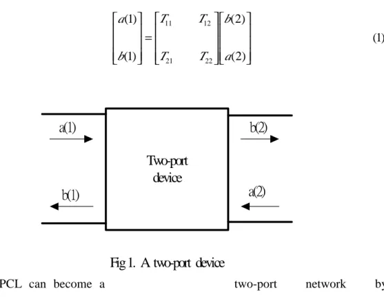
Fig. 1 shows a two port network, where a(1) and b(1) are the incident wave and reflected wave at port one and a(2) and b(2) are the incident wave and reflected wave at port two. These waves are interrelated through the chain scattering parameters, Tmn,
m,n=1,2, of a two port network as follows:
) 1 ( )
2 (
) 2 (
) 1 (
) 1 (
22 21
12 11
=
a b
T T
T T
b a
A PCL can become a two-port network by
terminating any two ports of the four-port configuration in either short-circuited or open-circuited formats. As a result, there are ten commonly elaborated combinations [12]. Fig. 2 shows a four-port PCL, where l is the physical length and Ii (i=1,2,3,4) is the terminal current at the respective port. In particular, the upper and lower lines in Fig. 2 have the same electrical characteristics.
The coupled lines in Fig. 2 can be decomposed into an even-mode excitation and an odd-mode excitation [13]. The overall circuit performance is the summation of the circuit responses due to both even-mode and odd-mode excitations. The impedance parameters concerned are as follows [12]:
Two-port device a(1)
b(1) a(2)
b(2)
Fig 1. A two-port device
) . 2 sec (
2
) . 2 sec (
2
) . 2 tan (
2
) . 2 tan (
2
, 0 0 32 23 41 14
, 0 0 42 24 31 13
, 0 0 43 34 21 12
, 0 0 44 33 22 11
j d Z Z Z
Z Z Z
j c Z Z Z
Z Z Z
j b Z Z Z
Z Z Z
j a Z Z Z
Z Z Z
o e
o e
o e
o e
θ θ θ θ
= +
= ′
= ′
= ′
′
= −
= ′
= ′
= ′
′
= −
= ′
= ′
= ′
′
= +
= ′
= ′
= ′
′
Fig. 2 One section of the parallel coupled line
where
Z
0e is the characteristic impedance of even-mode excitation,Z
0o is the characteristic impedance of odd-mode excitation. Notice thatθ is the electric length
of coupled-line withθ
=β l
;β
is the propagation constant andl is the physical
length.We can get impedance parameters of coupled lines in the Z domain by setting
θ j2
e
z
= . We obtain) . 3 ) (
1 (
) . 3 ) (
1 (
) . 3 ) (
1 ( 2
) 1 (
) . 3 ) (
1 ( 2
) 1 (
, 1 2 / 1 1 32 23 41 14
, 1 2 / 1 2 42 24 31 13
, 1
1 2 43 34 21 12
, 1
1 1 44 33 22 11
z d z Z c
Z Z Z
z c z Z c
Z Z Z
z b z Z c
Z Z Z
z a z Z c
Z Z Z
−
−
−
−
−
−
−
−
= −
= ′
= ′
= ′
′
= −
= ′
= ′
= ′
′
−
= +
= ′
= ′
= ′
′
−
= +
= ′
= ′
= ′
′
l
Por t 1 Por t 4
Por t 3 Por t 2
I
1I
2I
3I
4where
c
1 =Z
0e+Z
0o,c
2 =Z
0e −Z
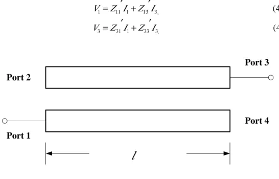
0o.Our object is to design a filter by using the parameters in the Z domain. For such a circumstance, we set I2
= I
4= 0. The circuit arrangement in Fig. 2 is thus changed to
that shown in Fig. 3. The four-port impedance matrix equations reduce to:) . 4 (
) . 4 (
3. 33 1 31 3
3, 13 1 11 1
b I
Z I Z V
a I
Z I Z V
+ ′
= ′
+ ′
= ′
Fig 3. Fundamental circuit of PCL
The four-port parallel coupled-lines now can be treated as a two–port network.
With a proper notation modification, the two-port impedance matrix can be expressed as follows
) 5 ( )
1 ( 2
) 1 ( )
1 (
) 1 ( )
1 ( 2
) 1 (
, 1
1 1 1
2 / 1 2
1 2 / 1 2 1
1 1
22 21
12 11
− +
−
−
− +
=
−
−
−
−
−
−
−
−
z z c z
z c
z z c z
z c
Z Z
Z Z
. Z Z and Z Z , Z Z , Z Z
where 11 = 11′ 12 = 13′ 21 = 31′ 22 = 33′
Furthermore, we can convert the impedance matrix into the chain scattering matrix (or T matrix) of a two-port network [12][14] with following equations
l
Por t 1
Por t 4 Por t 3 Por t 2
) . 6 2 (
] )
)(
][(
) )(
[(
4
) . 6 2 (
) )(
(
) . 6 2 (
) )(
(
) . 6 2 (
0 , 21
21 12 0 22 0 11 21 12 0 22 0 11 2 0 21 12 22
0 , 21
21 12 0 22 0 11 21
0 , 21
21 12 0 22 0 11 12
0 , 21 11
Z d Z Z
Z Z Z Z Z Z Z Z Z Z Z Z Z Z T Z
Z c Z
Z Z Z Z Z T Z
Z b Z
Z Z Z Z Z T Z
Z a Z T Z
∆
−
− +
− +
−
= −
− +
= −
−
−
− +
=
= ∆
where
∆ = Z
(Z
11 +Z
0)(Z
22 +Z
0)−Z
12Z
21.The chain scattering matrix is employed here because of its suitability for the cascade connection of two or more two-port networks. The corresponding T matrix of PCL is:
) 7 ) (
1 ( 8
1
1 , 1
1 1
1 2 / 1 0 2 22 21
12 11
−
= −
−
−
n p
n l
z z
Z T c
T
T T
where Z0 is the reference characteristic impedance and
2 2 2 2 2 1 2 2 2
1 1 0 1 0 1 2 0 1 0 1 0 ,
2 2 2 2 2 1 2 2 2
1 1 0 1 2 0 1 0 ,
2 2 2 2 2 1 2 2 2
1 1 0 1 0 1 2 0 1 0 1 0
(4 4 ) (2 4 8 ) ( 4 4 )
( 4 ) (2 4 8 ) ( 4 )
(4 4 ) (2 4 8 ) ( 4 4 ) .
l c Z c Z c c Z z c Z c Z z
n c Z c c Z z c Z z
p c Z c Z c c Z z c Z c Z z
− −
− −
− −
= + + + − − + − + +
= − + − + + −
= − − + + + + − − −
Notice that the denominator of each matrix element has the term (1−
z
−1) and the numerator of each matrix element is cast in the form ofα
0+α
1z
−1+α
2z
−2, whereα ,
0α and
1α are real numbers and they are functions of even-mode,
2odd-mode and reference characteristic impedances.
The overall chain-scattering parameter matrix of a cascade connection of parallel coupled lines is the sequential multiplication of the chain scattering matrix of each PCL, i.e.,
) 8 (
, ) ( 22 )
( 21
) ( 12 )
( 11
1 22
21
12 11
=
∏
= i i
i i
M
i
Network
T T
T T
T T
T T
where
M is the number of PCLs, T
11(i),T
12(i),T
21(i) andT
22(i) are the matrix elements representing the i-th element. If a circuit consists of M sections of PCLs, the matrix elementT
11,network(z) of the overall circuit is as follows) 9 ) (
1 ) (
(
, 1 2
/ 2
0 ,
11 M M
M
i
i i network
z z
z a z
T
− = −−
= ∑ −
where
a is a real number, and
ia
i is determined by reference characteristic impedanceZ
0, even-mode characteristic impedanceZ
0e and odd-mode characteristic impedance Z0o of every PCL.When the output port of the cascade network is properly terminated, we have a(2)=0. The transfer function
T
(z
) of such a network becomes) 10 ) (
1 (
) ( 1 ) 1 (
) 2 ) ( (
2
0 1 2
/ , 11
0 ) 2 (
i M
i i
M M
network a
z a
z z
z T
a z b T
−
=
−
−
=
∑
= −
=
=
where z−M/2 represents time delay of all PCLs. Equation (10) reveals that
T
(z
) has M zeros at z=1 (dc), which are contributed by M sections of PCLs. If all zeros in equation (10) are removed, the remaining part ofT
(z) can be regarded as an autoregressive (AR) process multiplied by z−M/2. If we express this corresponding AR process ofT
(z) asT
AR(z), we then have) 11 1 (
) (
, 2
0 i M
i i AR
z A z
T
−
∑
==
where
A
i =a
i.An AR process
T
AR(z)is solely characterized by the coefficientsA and these
i coefficients are determined by the modal characteristic impedances of coupled lines.If the zero locations of
T
(z) of the network are the same as that of an ideal filter )(
z
F
, we could makeT
AR(z) approximate a corresponding AR processF
AR(z)of the ideal filterF
(z) by adjusting the values of coupled-line impedances. This assures that the characteristic ofT
(z
) is close to that ofF
(z).3. Experimental Results
First of all, we select a discrete-time filter
F
(z)that satisfies the specification of required frequency response.F
AR(z) is obtained by dividingF
(z
) by the terms producing the zeros ofT
(z
). If bothT
(z) andF
(z
) have the same zero locations,(z)
F
AR can be expressed as follows) 12 1 (
) (
0 ,
∑
=′ −
= N
i
i i AR
z A z
F
where N is the order of the denominator of
F
(z),A
i′ is the denominator coefficients ofF
(z
). IfT
(z) andF
(z) do not have the same zeros locations, we find the equivalent AR processF
AR(z) by parametric modeling techniques.Since the magnitude of the delay term
z
−M/2 in equation (9) is equal to 1, we can neglect its influence on the magnitude consideration. We letT
AR(z
) approach(z)
F
AR by adjusting the values of even-mode characteristic impedances and odd-mode characteristic impedances of PCLs in a sense that 22 ( )
∑
i=MoA
i− A
i′
isminimized. If the coefficient difference between
T
AR(z) andF
AR(z
) is small enough, we argue that the transfer functionT
(z) of the PCL network and the systemfunction
F
(z
) of the ideal filter have similar magnitude responses in the frequency domain.A. Butterworth Band-pass Filter
A Butterworth band-pass filters is presented in this subsection. The central frequency of the filter is 3 GHz and the bandwidth is 5%.
A discrete-time Butterworth filter prototype is given as follows [9]
) 13 ( )
( 4
0 4
0
∑
∑
=
−
=
−
=
i
i i j
j j
z a
z b z
F
where {
b , 0
j ≤j
≤ 4}=1e-05×{0.0475, -0.1899, 0.2848, -0.1899, 0.0475}, and {a ,
i 0≤i
≤4}={ 1.0000, -0.0755, -2.8419, 0.0582, 2.7057}. Note that the filter prototype) (
z
F
shown in (13) is usually classified as a high-pass filter when it is used for discrete-time signal processing. However, when we unfold the magnitude function(z)
F
on the frequency axis,F
(z
) is a periodic function with a period of 2π . The filter prototypeF
(z) is a band-pass filter with its central frequency equal toπ . The
filter prototypeF
(z) has four zeros at z=1, which are to be realized by four sections of PCLs. We minimize the value of 28( )
∑
oA
i− A
i′
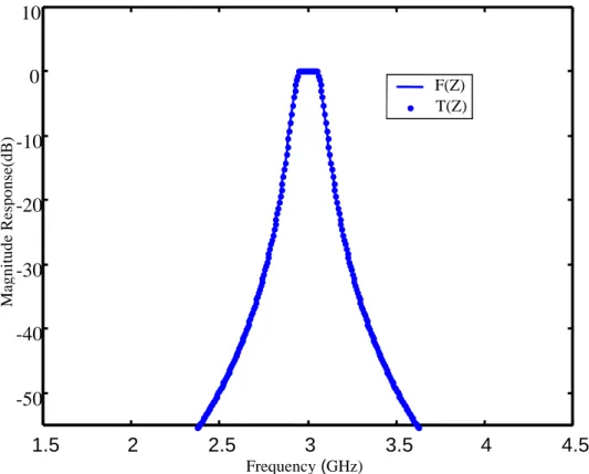
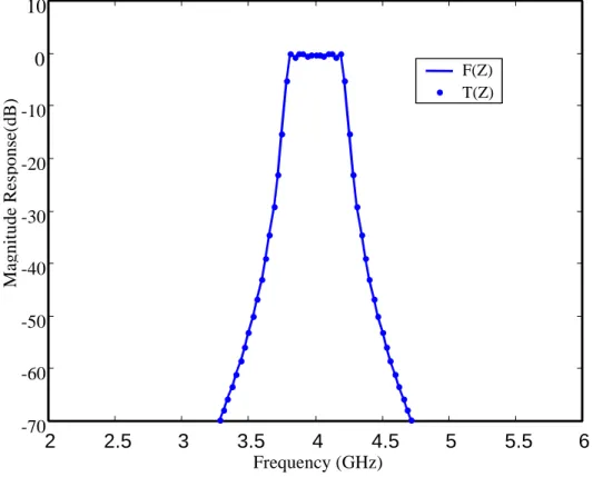
by adjusting the even-mode and odd-mode characteristic impedances of PCLs. As stated previously, a very small separation between two parallel lines is hard to realize in practical implementation. As a result, we set the limit so that the gap size is larger than 4 mil (0.1mm). Note that the gap size of each PCL is determined by even-mode and odd-mode characteristic impedances of PCL [15]. We therefore confine the upper bound and lower bound of even-mode and odd-mode characteristics impedances of coupled lines. The even-mode and odd-mode characteristic impedances of this four-section PCL are (69.45, 39.33)-(48.34, 43.07)-(61.06, 54.79)-(66.41, 40.51) ohms. In each parenthesis, the first number is the even-mode characteristic impedance and the second number isthe odd-mode characteristic impedance. When even-mode and odd-mode characteristic impedances are given, we get the line width and gap size of each PCL by using HP LineCalc tool [16]. The line width and gap size can also be obtained by using analytical formulations [15]. Ideally, each section of a PCL has the physical length of a quarter wavelength at 3 GHz. To consider fringing capacitance effect, the physical length of each section of PCL has been modified accordingly [17]. Fig. 4 shows the frequency responses of both the four-section coupled lines and ideal filter
) (
z
F
.Our program development environment is under Matlab signal processing toolbox and Optimization toolbox [11]. The optimization method involves the fmincon function in Matlab environment, wherein the optimization program consists of one main function and a sub-function executing the optimization. A typical program is composed about 100 command lines. The execution time is less than 3 minutes under Pentium-4 (1.4GHz) processor.
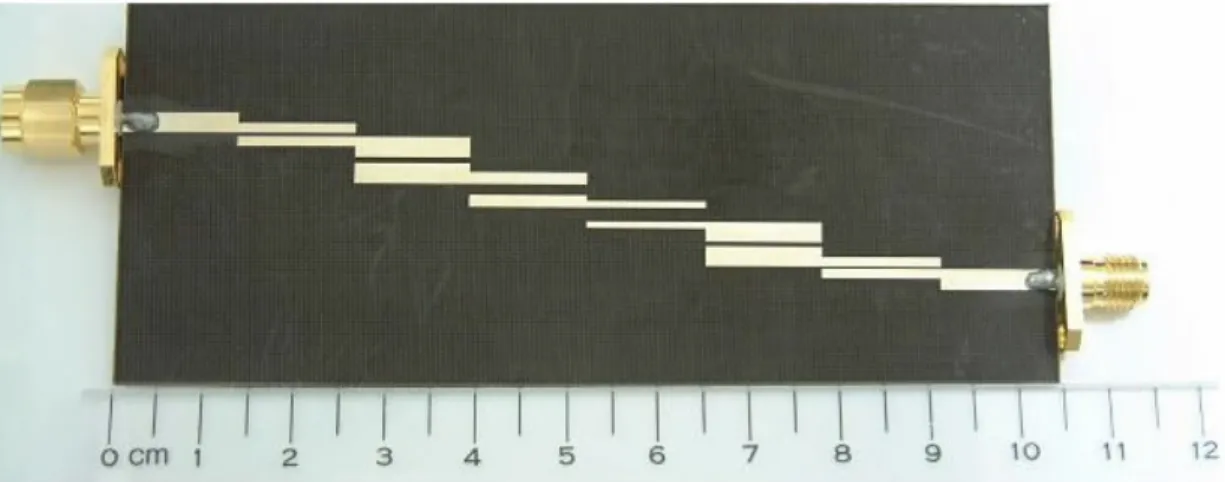
Fig. 5 shows the physical layout of the microstrip filter. The total length of the filter excluding the 50 ohms reference line on both sides is 68.13 mm. The filter was fabricated on a Duroid substrate having thickness
1.5 2 2.5 3 3.5 4 4.5 -50
-40 -30 -20 -10 0 10
Frequency (GHz)
Magnitude Response(dB)
F(Z) T(Z)
Fig. 4. The Magnitude responses of
F
(z
) andT
(z
) for the Butterworth band-pass with central frequency at 3.0 GHz and bandwidth of 5%.Fig. 5. Fabricated four-section PCL Butterworth band-pass filter with a center frequency of 3 GHz.
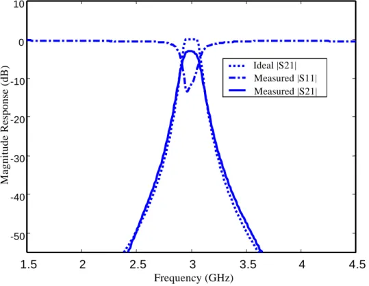
31 mil (0.79mm) and relative dielectric constant 2.5. On both sides of the filter, we place 50 ohms reference lines. Fig. 6 shows the measured scattering parameters
S
11and
S of the network shown in Fig. 5. The insertion loss is –2.8 (dB) in the
21 pass-band, which is due to both conductor and substrate losses [18].1.5 2 2.5 3 3.5 4 4.5
-50 -40 -30 -20 -10 0 10
Frequency (GHz)
Magnitude Response (dB)
Ideal |S21|
Measured |S11|
Measured |S21|
Fig. 6. Measured reflected and transferred scattering coefficients at input and output ports of the band-pass filter shown in Fig. 5.
B. Chebyshev Band-pass Filter
A discrete-time Chebyshev band-pass filter is elaborated in this subsection. The ripple in the pass-band is 0.5 (dB), the central frequency is 4 GHz and the bandwidth is 10 %.
A discrete-time Chebyshev filter prototype is given as follows [9]
) 15 ( )
( 6
0 6
0
∑
∑
=
−
=
−
=
i
i i j
j j
z a
z b z
F
where {
b , 0
j ≤j
≤6}=1e-6×{0.0159, -0.0955, 0.2387, -0.3182, 0.2387, -0.0955, 0.0159}, and {a , 0
i ≤i
≤6}={1.0000, -0.1168, -4.7526, 0.2900, 9.1203, -0.1093, -8.8151}. The filter prototypeF
(z) has six zeros atz=1, which can be realized by
six sections of PCLs. We minimize the value of 212( )
∑
oA
i− A
i′
by adjusting even-mode and odd-mode characteristic impedances of all PCLs. The even-mode and odd-mode characteristic impedances of this six-section PCL are (93.49, 60.25)-(55.23, 43.05)-(75.61, 63.18)-(102.77, 88.98)-(58.22, 42.60)-(98.21, 53.84) ohms. In each parenthesis, the first number is the even-mode characteristic impedance and the second number is the odd-mode characteristic impedance. Ideally, each section of PCL has physical length of a quarter wavelength at 4 GHz. However, the physical length of each section of PCL should be modified to count for the fringing capacitance effect. Fig. 7 shows the frequency responses of both the six-section coupled line and ideal filterF
(z).2 2.5 3 3.5 4 4.5 5 5.5 6
-70 -60 -50 -40 -30 -20 -10 0 10
Frequency (GHz)
Magnitude Response(dB)
F(Z) T(Z)
Fig. 7. The Magnitude responses of
F
(z
) andT
(z
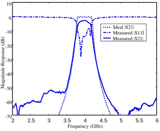
) for the Chebyshev band-pass with central frequency at 4.0 GHz and bandwidth of 10%.Fig. 8 shows the physical layout of the microstrip filter, and the total length of the filter excluding the 50 ohms reference line on both sides is 77.9 mm. The filter is fabricated on a Duroid substrate having thickness 31 mil (0.79mm) and relative dielectric constant 2.5. Fig. 9 shows the measured scattering parameters
S
11 andS of the network shown in Fig. 8. The insertion loss is –2.9 (dB) in the
21 pass-band, which is mainly due to both conductor and substrate losses [18]. Obviously, the measured results are in good agreement with the numerical values via HP ADS simulation tool [19].Fig. 8. Fabricated six-section PCL Chebyshev type I band-pass filter with a center frequency of 4 GHz.
4. Conclusion
The parameters of parallel coupled lines were expressed in the Z domain. In addition, a novel methodology was developed to design filters by using Z domain transfer function and optimization method. The close agreement between theoretical values and experimental results had illustrated the validity of this novel method.
2 2.5 3 3.5 4 4.5 5 5.5 6 -70
-60 -50 -40 -30 -20 -10 0 10
Frequency (GHz)
Magnitude Response (dB)
Ideal |S21|
Measured |S11| Measured |S21|
Fig. 9. Measured reflected and transferred scattering coefficients at input and output ports of the band-pass filter shown in Fig. 8.
5. Reference
[1] Gaobiao Xiao; Yashiro, K.; Ning Guan; Ohkawa, S. “An effective method for designing nonuniformly coupled transmission-line filters “
IEEE Trans.
Microwave Theory Tech., Vol. 49 pp.1027-1031 , June 2001.
[2] M. L. Roy, et. Al., “The continuously varying transmission-line tecnique-application to filter design,”
IEEE Trans. Microwave Theory Tech., vol. 47, pp. 1680-1687, Sept.
1999.
[3] Drozd, J.M.; Joines, W.T. “Maximally flat quarter-wavelength-coupled transmission-line filters using Q distribution,”
IEEE Trans. Microwave Theory
Tech., Volume: 45 Issue: 12 Part: 1 , pp. 2100 –2113, Dec. 1997.
[4] Chi-Yang Chang; Cheng-Chung Chen; Hong-Jie Huang “Folded quarter-wave resonator filters with Chebyshev, flat group delay, or quasi-elliptical function response,”
Microwave Symposium Digest, 2002 IEEE MTT-S International, pp.
1609-1612 vol. 3. 2002.
[5] R. Levy and J. D. Rhodes, “A combline elliptic filter,”
IEEE Trans. Microwave Theory Tech. Vol. 19, pp. 26-29, Jan. 1971.
[6] Da-Chiang Chang, Ching-Wen Hsue “Wide-band equal-ripple filters in nonuniform transmission lines,”
IEEE Trans. Microwave Theory Tech., Vol. 50 ,
pp. 1114-1119 , April 2002[7] P. I. Richard, “Resistor-transmission line circuits,”
Proc. IRE, vol, 36, pp.
217-220, Feb, 1948.
[8] K. Kuroda, “General properties and synthesis of transmission-line nerworks,”
in Microwave Filters and Circuits, A. Mstsumoto, Ed. New York: Academic, 1970,
vol. 22.[9] A. V. Oppenheim, R. W. Schafer, Discrete-Time Signal Processing. Englewood Cliffs, NJ:Prentice-Hall., 1998.
[10] S. Haykin, Adaptive Filter Theory. Englewood Cliffs, NJ: Pretice-Hall, 1996.
[11] T. Coleman, M. A. Branch, A. Grace,
Optimization Toolbox. The Math Works
Inc.,User’s Guide Version 2. Natick, MA, 1999.[12] D. M. Pozar, Microwave Engineering, 2nd ed. New York: Wiley, 1998.
[13] Robert S. Elliott,
An Introduction to Guided Waves and Microwave Circuits.
Prentice-Hall, 1993.
[14] R.E Collin, Foundation for Microwave Engineer. New York: McGraw-Hall, Inc., 1993.
[15] S. Akhtarzad, T. R. Rowbotham and P. B. Johns, “The design of coupled microstrip lines,”
IEEE Trans. Microwave Theory Tech., vol. 23, No. 6, pp.
486-492, June 1975.
[16] D. Turner, R. Wilhelm, W. Lemberg, Line Calc. Agilent Technologies. Palo Alto, CA, 2000.
[17] S. B. Cohn, “Parallel transmission-line-resonator filters”, IRE Trans. MTT, vol.
MTT-6, pp. 223-231, April 1958.
[18] Sheng-Yuan Lee, Chih-Ming Tsai, “New cross-coupled filter design using improved hairpin resonators”
IEEE Trans. Microwave Theory Tech., Vol. 48,
pp.2482-2490 , Dec 2000.[19] D. Turner, R. Wilhelm, W. Lemberg,
Advanced Design System. Agilent
Technologies. Palo Alto, CA, 2000.Figure Captions for “Z-Domain Representations of Parallel Coupled Lines and Their Applications to Filters”
Fig. 1 A two-port device
Fig. 2 One section of the parallel coupled line
Fig. 3 Fundamental circuit of PCL
Fig. 4 The Magnitude responses of
F
(z
) andT
(z
) for the Butterworth band-pass with central frequency at 3.0 GHz and bandwidth of 5%.Fig. 5 Fabricated four-section PCL Butterworth band-pass filter with a center frequency of 3 GHz.
Fig. 6 Measured reflected and transferred scattering coefficients at input and output ports of the band-pass filter shown in Fig. 5.
Fig. 7 The Magnitude responses of
F
(z
) andT
(z
) for the Chebyshev band-pass with central frequency at 4.0 GHz and bandwidth of 10%.Fig. 8 Fabricated six-section PCL Chebyshev type I band-pass filter with a center frequency of 4 GHz.
Fig. 9 Measured reflected and transferred scattering coefficients at input and output ports of the band-pass filter shown in Fig.