Sensing Performance of EGFET PH Sensors with CuO Nanowires Fabricated on Glass Substrate
Tsung-Han Yang, Sheng-Po Chang*, Chih-Wei Li, and Shoou-Jinn Chang
Institute of Microelectronics & Department of Electrical Engineering Center for Micro/Nano Science and Technology
Advanced Optoelectronic Technology Center National Cheng Kung University, Tainan 70101, Taiwan
In this work, the sensing membrane of extended-gate field-effect-transistor (EGFET) pH sensors with an intrinsic copper oxide (CuO) nanowire array was fabricated on a glass substrate by directly heating a Cu film at 450°C for 5 h in air. It was found that the average length and average diameter of these nanowires (NWs) were 2.5 μm and 70 nm, respectively. The resulting EGFET pH sensors with CuO NWs exhibited significantly improved sensing performances owing to the large sensing surface-to-volume ratio. The pH sensitivity calculated from the linear relation between the drain-source current and the pH value was 23.5 μA/pH and that calculated from the linear relation between the reference voltage and the pH value was 18.4 mV/pH.
Keywords: CuO, Nanowire, EGFET
*E-mail: changsp@mail.ncku.edu.tw
1. Introduction
Recently, there has been great interest in human health issues owing to irregular living and dietary habits. Because the pH value of blood is an important index for the human body, even a small change in the pH of body fluids can signal a problem in the human body. Biosensors based on the pH sensor have many applications such as blood monitoring, environment monitoring, biological analyses, chemical analyses, and clinical detection [1–3]. Extended-gate field-effect-transistors (EGFETs) offer several advantages such as easy fabrication, small influence of optical illumination and operation temperature, and disposable gate. Therefore, EGFETs have been widely used in biosensors [4, 5]. EGFETs consist of two parts: a metal-oxide-semiconductor field-effect-transistor (MOSFET) and a sensing membrane.
Recently, several materials have been widely used as the sensing membrane in EGFET pH sensors [6–8]. Unlike most n-type metal oxides, CuO with a narrow bandgap of 1.2 eV is a p-type material with a monoclinic structure [9, 10]. Owing to these properties, CuO is used in high temperature superconductors [11], magnetic storage media [12], heterogeneous catalysts [13], field emitters [14], and gas sensors [15]. Recently, one-dimensional (1D) nanowires have attracted a lot of attention. With the same volume, one-dimensional (1D) nanowires (NWs) can provide a much larger surface area as compared to bulk and thin film materials. Thus, 1D NW-based chemical sensors normally exhibit high sensitivity, especially in semiconducting metal oxide sensors [16–18]. CuO nanowires can be grown by various processes such as liquid–liquid method [19] and catalyzed synthesis [20]. Recently, Jiang et al. proposed a simple method for the preparation of CuO NWs wherein copper sheets are directly heated in air [21]. However, currently, the direct growth of CuO nanowires on copper sheets is not easy during device integration. To solve this problem, CuO NWs should be directly grown on silicon or glass substrates. Indeed, it has been shown that CuO NWs can be grown directly on silicon substrates coated with a copper layer [22–24]. Compared with silicon substrates, glass substrates are low in cost and are available in large sizes.
Thus, glass is an ideal substrate material for device applications.
Here, in order to fabricate the sensing membrane of EGFETs, CuO NWs were deposited by directly heating a Cu film in air. We achieved enhanced response from the NW-based pH sensors owing to the large surface-to-volume ratio.
2. Experiment
1. Fabrication of CuO EGFET pH sensor
For the fabrication of the EGFET sensors, before growing the CuO NWs, glass substrates were wet-cleaned by acetone and deionized water and then baked at 100°C for 10 min to remove moisture. A 100-nm-thick CuO layer was first deposited onto the glass substrates by DC sputtering to serve as the adhesion and conducing layer. We maintained the flow rates of Ar and O
2at 15 and 6 sccm, respectively. A pure copper thin film with a thickness of 0.5 μm was subsequently deposited on top of the CuO layer. The samples were then placed in a furnace and annealed at 450°C in air for 5 h to grow CuO NWs.
The procedure used to grow the CuO NWs is schematically shown in Fig. 1.
Fig. 1. Procedure used to grow CuO NWs and procedure used to fabricate CuO-NW pH sensors.
An X-ray diffractometer (XRD) was then used to characterize the crystallography for various thicknesses (0.1, 0.3, 0.5, 1, 2, and 3 μm) of the Cu thin film and 100-nm-thick CuO layer. The surface morphology of the samples and the size distribution of the NWs were characterized using a field-emission scanning electron microscope (FESEM).
2. Measurement System
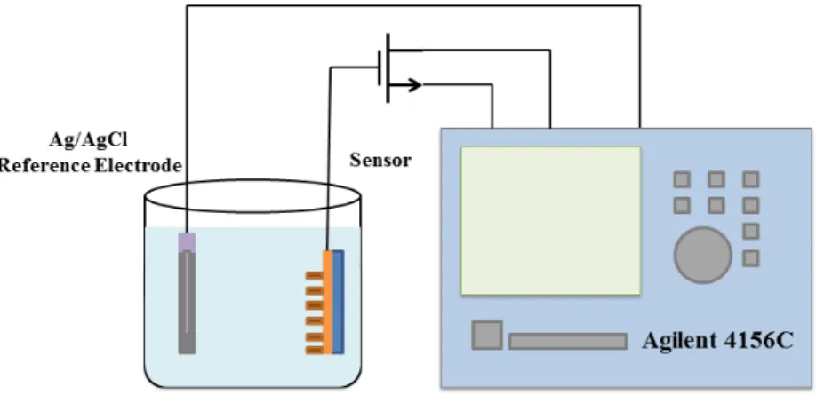
To measure the sensing performances of the fabricated pH sensors, the pH sensor and the Ag/AgCl reference electrode were dipped into the detection solution (pH value varied from 4 to 10). The CuO conducting layer of the EGFET was connected to the gate of a commercial MOSFET device. The sensing response of the pH sensors was measured using an Agilent 4156C analyzer. The measurement system is shown in Fig. 2.
Fig. 2. Measurement system of CuO EGFET pH sensor.
3. Results and Discussion
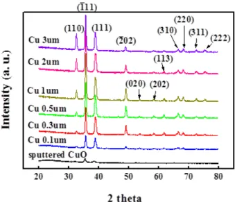
Fig. 3 shows the XRD spectra measured from the CuO layer and the thermally treated sample. It shows that only peaks
related to CuO (110) and (111) were observed from the CuO layer. After copper film deposition and furnace annealing, we
also observed peaks related to CuO (202), (113), (310), (220), (311), and (222) from the thermally treated sample. These
peaks suggest that the copper layer was completely oxidized into CuO by furnace annealing in air at 450°C for
Fig. 3. XRD spectra measured from CuO layer and thermally treated sample.
5 h. Moreover, it was found that the intensities of the peaks observed from the CuO layer were much weaker than those observed from the thermally treated samples. This was attributed to the much smaller thickness of the CuO layer as compared to that of the pure copper layer. Figs. 4(a) and (b) show cross-sectional and top-view scanning electron microscopy (SEM) images of the thermally treated sample with a Cu layer thickness of 0.5 μm. After thermal treatment, it was found that high-density vertically aligned NWs were grown on the CuO/glass substrate. From these SEM images, it was found that the average length and average diameters of these NWs were 2.5 μm and 70 nm, respectively.
Fig. 4. (a) Cross-sectional and (b) top-view SEM images of thermally treated sample with Cu layer thickness of 0.5 μm.
To investigate the sensing performance, we used the site binding model [25], [26]. The changes in the surface potential were determined from the pH value of the electrolyte solution. According to the site binding model, the surface potential voltage (ψ
0) between the sensing layer and the electrolyte interface can be expressed as [27]
0 1 01
2.303 sinh
, (1)
pzc
q q
pH pH
kT kT
where pH
PZCis the pH value at the point of zero charge, q is the electron charge, k is the Boltzmann constant, T is the
absolute temperature, and β is the sensitivity parameter. The relation between β and the number of surface sites per unit
area (N
S) can be given as [27]
2 1
2 ( )
2, (2)
S a bDL
q N K K
kTC
where K
a and Kb are the acid equilibrium constant and basic equilibrium constant, respectively, and CDL is the capacitanceof the electrical double layer, as derived from the Gouy–Chapman–Stern model [28]. By increasing the sensitivity parameter β, a better linear response between surface potential voltage and pH value can be obtained.
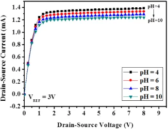
The measured dependence of the drain-source current (I
DS) on the drain-source voltage (V
DS) of the EGFET with CuO NWs (length = 2.5 μm) operated at a reference electrode voltage (V
REF) of 3 V is shown in Fig. 5. The experimental results
showed that I
DSdecreased with an
Fig. 5. Drain-source current vs. drain-source voltage characteristics of pH sensor with CuO NWs.
increase in the pH value of the detection solution. This dependence was attributed to the accumulation of H
+ions on the
sensing surface in the acidic solution, which was equivalent to applying an extra positive voltage at the gate of the
MOSFET. On the other hand, the I
DSdecreased with the pH value in the basic solution due to the accumulation of OH
—ions, which was equivalent to application of an extra negative voltage at the gate of the MOSFET. Therefore, we concluded
that the drain-source current can be modulated by varying the pH value of the detection solution. Based on the results
shown in Fig. 5, the measured drain-source current as a function of pH value is shown in Fig. 6, where the drain-source
voltage (V
DS) of the MOSFET was 4 V and the reference electrode voltage (V
REF) was 3 V. The pH sensitivity was
calculated from the linear relation between the drain-source current and the pH value. The sensing sensitivity of the pH
sensors with CuO NWs was 23.5 μA/pH.
Fig. 6. Drain-source current as a function of pH value.
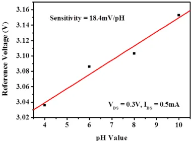
Fig. 7 shows the drain-source current–reference voltage (I
DS–V
REF) characteristics of the pH sensor with CuO NWs operated at V
DS= 0.3 V. According to the experimental results, the associated threshold voltage (V
TH) shifted to a higher reference voltage with an increase in the pH value. The obtained reference voltage is shown as a function of the pH value in Fig. 8. The sensitivity was defined as the dependence of the obtained reference voltage on the pH value. The sensitivity was calculated from the linear relation between the reference voltage and the pH value. From the experimental results shown in Fig. 8, the sensitivity of the pH sensors with CuO NWs was found to be 18.4 mV/pH.
Fig. 7. Drain-source current vs. reference voltage characteristics of pH sensor with CuO NWs.
Fig. 8. Reference voltage as a function of pH value.
4. Conclusion
In this work, using CuO as the adhesion and conducting layer, we successfully grew CuO NWs as the sensing area of pH sensors by thermally annealing at 450 °C for 5 h in air. It was found that the average length and average diameter of these NWs were 2.5 μm and 70 nm, respectively. The resulting EGFET pH sensors with CuO NWs exhibited significantly improved sensing performance owing to the large sensing surface-to-volume ratio. The sensing sensitivity calculated from the linear relation between the drain-source current and the pH value was 23.5 μA/pH and that calculated from the linear relation between the reference voltage and the pH value was 18.4 mV/pH.
Acknowledgments: The authors would like to thank the National Science Council and Bureau of Energy, Ministry of
Economic Affairs of Taiwan, R.O.C. for the financial support under Contract No. 100-2221-E-006-168 and 101-D0204-6
and the LED Lighting Research Center of NCKU for the assistance of device characterization. This work was also
supported in part by the Center for Frontier Materials and Micro/Nano Science and Technology, the National Cheng Kung
University, Taiwan. This work was also supported in part by the Advanced Optoelectronic Technology Center, the National
Cheng Kung University, under projects from the Ministry of Education.
References
1. X. S. Fang et al., Prog. Mater., Sci., 56 (2011) 175
2. Q. Shao et al., Appl. Surf. Sci., 257 (2011) 5559
3. X. S. Fang, L. M. Wu, and L. F. Hu, Adv. Mater., 23 (2011) 585 4. L. L. Chi et al., Mater. Chem. Phys., 63 (2000) 19
5. B. S. Kang et al., Appl. Phys. Lett., 91 (2007) 252103
6. E. M. Guerra, G. R. Silva, and M. Mulato, Solid State Sci., 11 (2009) 456 7. C. L. Li et al., Appl. Phys. Lett., 84 (2004) 2676
8. L. T. Yin et al., Sensor Actuat. B-Chem., 71 (2000) 106 9. A. E. Rakhshani, Solid State Electron., 29 (1986) 7
10. B. Balamurugan and B. R. Mehta, Thin Solid Films, 396 (2001) 90 11. A. H. MacDonald, Nature, 414 (2001) 409
12. H. M. Fan et al., Nanotechnol., 15 (2004) 37
13. J. B. Reitz and E. I. Solomon, J. AMCS, 120 (1998) 11467 14. C. T. Hsieh et al., Appl. Phys. Lett., 83 (2003) 3383 15. Y. S. Kim et al., Sensor Actuat. B-Chem., 135 (2008) 298 16. Z. P. Sun et al., Nanotechnol., 17 (2006) 2266
17. Q. Wan, et al., Appl. Phys. Lett., 84 (2004) 3654 18. E. Comini et al., Appl. Phys. Lett., 81 (2002) 1869
19. P. Saravanan, S. Alam, and G. N. Mathur, Thin Solid Films, 491 (2005) 168 20. C. M. Tsai et al., Acta Mater., 57 (2009) 1570
21. X. Jiang, T. Herricks, and Y. Xia, Nano Lett., 2 (2003) 1333 22. S. C. Yeon et al. J. Vac. Sci. Tech. B, 24 (2006) 940 23. K. L. Zhang et al., Nanotechnol., 18 (2007) 275607 24. Y. W. Park et al., J. Electrochem. Soc., 157 (2010) K119
25. D. E. Yates, S. Levine, and T. W. Healy, J. Chem. Soc. Faraday Trans. 1,70 (1974) 1807 26. R. E. G. Van Hal et al., Sens. Actuator B, 24 (1995) 201
27. H. K. Liao et al. Mater. Chem. Phys., 59 (1999) 6 28. K. B. Oldham, J. Electro. Chem., 613 (2007) 131