行政院國家科學委員會專題研究計畫 期中進度報告
新穎光電半導體材料,低維度奈米微細結構及其元件構造之 光學特性研究(1/3)
計畫類別: 個別型計畫
計畫編號: NSC94-2215-E-011-002-
執行期間: 94 年 08 月 01 日至 95 年 07 月 31 日 執行單位: 國立臺灣科技大學電子工程系
計畫主持人: 黃鶯聲
計畫參與人員: 陳麒安
報告類型: 精簡報告
處理方式: 本計畫可公開查詢
中 華 民 國 95 年 5 月 30 日
行政院國家科學委員會補助專題研究計畫 □ 成 果 報 告
■期中進度報告
新穎光電半導體材料,低維度奈米微細結構及其元件構造之光 學特性研究(1/3)
Optical Properties Study of Novel Optoelectronic Semiconductor Materials, Low Dimensional Nanostructures and Device Structures
計 畫 類 別 : ■ 個 別 型 計 畫 □ 整 合 型 計 畫 計 畫 編 號 : NSC 94 - 2215 - E - 011 - 002 執行期間: 94 年 8 月 1 日 至 95 年 07 月 31 日
計 畫 主 持 人 : 黃 鶯 聲
計畫參與人員:陳麒安
國立台灣科技大學電子工程所博士班研究生
成果報告類型(依經費核定清單規定繳交):■精簡報告 □完整報告
本 成 果 報 告 包 括 以 下 應 繳 交 之 附 件 :
□ 赴 國 外 出 差 或 研 習 心 得 報 告 一 份
□ 赴 大 陸 地 區 出 差 或 研 習 心 得 報 告 一 份
□ 出 席 國 際 學 術 會 議 心 得 報 告 及 發 表 之 論 文 各 一 份
□ 國際合作研究計畫國外研究報告書一份
處理方式:除產學合作研究計畫、提升產業技術及人才培育研究計畫、列管計畫 及下列情形者外,得立即公開查詢
□涉及專利或其他智慧財產權,□一年□二年後可公開查詢
執行單位:國立台灣科技大學電子工程所
中 華 民 國 95 年 5 月 30 日
一、 中文摘要
本期計畫目的主要利用調制光譜及表面光電壓量測技巧來研究 II-VI 族半導體化合物,
III-V 族 GaAsSb/GaAs 多重量子井結構及 InAs 量子點半導體微細結構。
在II-VI族半導體化合物方面,利用電場調制(CER及PR)光譜檢查高壓布里奇曼法所成長之 wurtzite結構Cd1–x–yBexZnySe樣品之能帶特性。在GaAsSb量子井中,我們利用電場調制(PT)及波 長調制(WMSPS)光譜量測經由Sb中斷成長之GaAsSb/GaAs量子井中各個躍遷位置變化情形,並 分析探討其原因。在InAs 量子點中,利用表面光電壓(SPS)及光激螢光(PL)光譜分析不同space layer厚度多重堆疊之InAs量子點特性。
關鍵詞:電場調制、II-VI 族寬能隙半導體、GaAsSb/GaAs 量子井、InAs 量子點。
Abstract
Cd1–x–yBexZnySe mixed alloys were characterized by contactless electroreflectance (CER) and photoreflectance (PR). The temperature coefficients were determined via Varshni and Bose-Einstein fit. The effect of the growth interruptions on GaAsSb/GaAs multiple quantum wells (MQWs) was investigated by phototransmittance (PT) and wavelength-modulated surface photovoltage spectroscopy (WMSPS). The influence of the interband transition of GaAsSb/GaAs MQWs were observed and the parable origins were also discussed. The multiple stacked InAs quantum dots (QDs) were characterizaed by surface photovoltage spectroscopy (SPS) and photoluminescence (PL). The effect of the multiple stacked InAs QDs was discussed.
Keywords : electromodulation, II-VI wide band gap material, GaAsSb/GaAs MQWs, InAs QDs.
二、計畫緣由與目的
近幾年來, II-VI 寬能隙半導體材料逐漸在光電產業上受到注意,因其發光波長為 較短波長屬藍光到紫外波段,可應用於照明光源系統、大型全彩看板。因其實用性所
以目前有極多數的機構均在研究寬能隙系列的材料。近年來 GaAsSb/GaAs 量子井及
InAs 量子點材料系統被開發為應用於長波長光纖傳輸系統之光源,若能利用非破壞性 光學檢測方法來檢測此一新穎材料值得探討。對業界可有相當助益。
三、研究方法及計畫成果
研究方法
1. 利 用 非 接 觸 式 電 場 調 制 (CER) 及 光 子 調 制 (PR) 反 射 光 譜 來 得 到 Cd1–x–yBexZnySe 材 料 之
(A), (upper band) (B), (lower band) (C)之躍遷訊號。藉由溫度變化量
測來得到A, B及C躍遷訊號位置及展寬參數隨溫度變化的情形。
C V
7
9 →Γ
Γ Γ7V →Γ7C Γ7V →Γ7C
2.利用電場調制(PT)及波長調制(WMSPS)光譜量測經由 Sb 中斷成長之 GaAsSb/GaAs 量子井中 各個躍遷位置變化情形,並與理論計算結果比較,探討其可能原因。
3.利用表面光電壓(SPS)及光激螢光(PL)光譜分析多堆疊層之 InAs 量子點訊號。分析不同 space layer 厚度之多堆疊 InAs 量子點訊號變化情形。
四、結果與討論
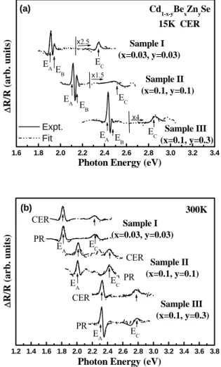
利用CER和PR技巧量測不同Be及Zn含量之Cd1–x–yBexZnySe單晶樣品可正確地得到
(A), (upper band) (B), (lower band) (C)之躍遷訊號,在溫度變化(15K-400K)的量測
中,發現加入Be後使躍遷訊號隨溫度變化的程度較快。另一方面,利用PT及WMSPS光譜觀察 以Sb為成長中斷氣體之GaAsSb/GaAs 量子井結構,發現其量子井中躍遷訊號隨著中斷增加而紅 移。此一現象推測為在GaAsSb/GaAs量子井介面有多餘Sb的殘存造非陡峭之介面型式,使量子 井介面區域加寬及Sb含量增加。利用表面光電壓(SPS)及光激螢光(PL)光譜分析不同space layer 厚度多重堆疊之InAs量子點特性。當space layer的厚度減少,InAs量子點的躍遷訊號有藍移的 現象為應力所造成的intermixing.
C V
7
9 →Γ
Γ
V
Γ7 →Γ7C Γ7V →Γ7C
五、計畫成果自評
此期計劃中,總共發表與計劃相關論文數篇,成果豐碩。
六、參考文獻
1. L. Malikova, W. Krystek, F. H. Pollak, N. Dai, A. Cavus and M. C. Tamargo, Phys.. Rev. B, 54 1819 (1996).
2. W. Paszkowicz, K. Godwod, J. Domagała, F. Firszt, J. Szatkowski, H. Męczyńska, S. Łęgowski, and M. Marczak, Solid State Commun. 107, 735 (1998).
3. C. H. Hsieh, Y. S. Huang, C. H. Ho, K. K. Tiong, M.Muňoz, O. Maksimov, and M. C. Tamargo, Jpn. J. Appl. Phys. 43, 459 (2004).
4. G. Liu, S. L. Chuang, and S. H. Park, J. Appl. Phys. 88 5554 (2000).
5. Gh. Dumitras and H. Riechert, J. Appl. Phys. 94 3955 (2003).
6. G. S. Solomon, J. A. Trezza, A. F. Marshall, and J. S. Harris, Phys. Rev. Lett. 76, 952 (1996).
7. J. Bhattacharyya, S. Ghosh, S. Malzer, G. H. Döhler, and B. M. Arora, Appl. Phys. Lett. 87, 212101 (2005).
8.
研究計畫相關成果:
1. Liu,Y. T., P. Sitarek, P. J. Huang, Y. S. Huang, F. Firszt, S. Legowski, H. Meczynska, A.
Marasek, and W. Paszkowicz, “Optical Characterizationof Cd1-x-yBexZnySe Mixed Crystals,” phys.
stat. sol. (c) , Vol.3, pp.734-737 (2006).
2. Huang, P. J., P. Sitarek, Y. S. Huang, O. Maksimov, M. C. Tamargo, F. Firszt, and H. Meczynska,
“Characterization of BexCd1-xSe Alloys by Contactless Electroreflectance,” phys. stat. sol. (c), Vol.3, pp.738~741 (2006).
3. Huang, P. J., Y. S. Huang, F. Firszt, H. Męczyńska, and K.K. Tiong, “Temperature dependence of the band edge excitonic transitions of a wurtzite-type Cd0.925Be0.075Se mixed crystal,” Solid State Communications, Vol.273, pp.82~86 (2006).
4. C. H. Chan , H. S. Chen , C. W. Kao, H. P. Hsu, Y. S. Huang, J. S. Wang, “ Investigation of multiplayer electronic vertically coupled InAs/GaAs quantum dots structures using surface photovoltage spectroscopy, “ Appl. Phys. Lett., under revision (2006).
5. H. P. Hsu, P. Sitarek, Y. S. Huang, P. W. Liu, J. M. Lin,H. H. Lin, and K K Tiong, ” Modulation spectroscopy study of the effects of growth interruptions on the interfaces of GaAsSb/GaAs multiple quantum wells,” J. Physics: Conden. Matter, under revision (2006).
附圖:
1.6 1.8 2.0 2.2 2.4 2.6 2.8 3.0 3.2 3.4
EB EB
EA EA
EC EC (a)
Sample III (x=0.1, y=0.3) Sample II (x=0.1, y=0.1) Sample I (x=0.03, y=0.03) EC
EB EA
x4 x1.5 x2.5
Expt.
Fit
Cd1-x-yBexZnySe 15K CER
ΔR/R (arb. units)
Photon Energy (eV)
1.2 1.4 1.6 1.8 2.0 2.2 2.4 2.6 2.8 3.0 3.2 3.4 3.6 3.8
EC EC
EA EA
CER CER
PR
PR (b)
EC PR
CER EA
Sample III (x=0.1, y=0.3) Sample II (x=0.1, y=0.1) Sample I
(x=0.03, y=0.03) 300K
ΔR/R (arb. units)
Photon Energy (eV)
Fig. 1 (a) Experimental (dashed lines) CER spectra at 15 K and (b) the CER and PR spectra of Cd0.94Be0.03Zn0.03Se (sample I), Cd0.8Be0.1Zn0.1Se (sample II) and Cd0.6Be0.1Zn0.3Se (sample III) at 300 K. The solid lines are fits to the first derivative of Lorentzian lineshape functional form. The obtained values of the energies are indicated by the arrows.
0 50 100 150 200 250 300 350 400 450 500 550 600 1.7
1.8 1.9 2.2 2.3
2.4 Sample I
Cd0.94Be
0.03Zn
0.03Se
EA Expt.
EA Expt.-ΔEth EB Expt.
EB Expt.-ΔEth EC Expt.
EC Expt.-ΔEth Fit to Eq.(3a) Fit to Eq.(3b)
Energy (eV)
Fig. 2 The temperature dependence of EA (open squares), EB (open circles), and EB C (open triangles) of (a)
Cd0.94Be0.03Zn0.03Se (Sample I), with representative error bars. The solid squares, circles and triangles are the data minus the thermal expansion contribution, ΔEth(T). The dashed and solid lines are least-squares fits to Varshni equation.
Fig. 3. The PT spectra (full lines) from three GaAs1-xSbx/GaAs samples taken at 300 K. The open circles are the least- squares fits to the FDLL line shape function. The obtained energy values are denoted by arrows.
Figure 4. The WMSPS spectra (full lines) from three GaAs1-xSbx/GaAs samples taken at 300 K. The open circles are the least-squares fits to the FDLL line shape function. The obtained energy values are denoted by arrows.
Fig. 5 Room temperature SPS spectra of 30 layers vertically stacked InAs/GaAs QDs with different SL and the reference structure with one QD layer. Arrows show QD related transition energies determined from the fitting.
Fig. 6 The TEM image of the EVCQDs structure with 15 nm SL thickness.