行政院國家科學委員會專題研究計畫 成果報告
大晶粒低溫多晶矽膜之製程設計暨膜質分析與系統評估
計畫類別: 個別型計畫
計畫編號: NSC94-2212-E-011-023-
執行期間: 94 年 08 月 01 日至 95 年 07 月 31 日 執行單位: 國立臺灣科技大學電子工程系
計畫主持人: 葉文昌
計畫參與人員: 柯敦元, 黃祥恩, 周明賜
報告類型: 精簡報告
報告附件: 出席國際會議研究心得報告及發表論文 處理方式: 本計畫可公開查詢
中 華 民 國 95 年 10 月 16 日
行政院國家科學委員會補助專題研究計畫成果報告 大晶粒低溫多晶矽膜之製程設計暨膜質分析與系統評估
計畫類別:□ 個別型計畫 □ 整合型計畫
計畫編號:NSC-94-2212-E-011-023-大晶粒低溫多晶矽膜之製程設計暨 膜質分析與系統評估
執行期間:2005 年 8 月 1 日至 2006 年 7 月 31 日
計畫主持人:葉文昌 共同主持人:
計畫參與人員: 柯敦元, 黃祥恩, 周明賜
成果報告類型(依經費核定清單規定繳交):精簡報告 本成果報告包括以下應繳交之附件:
V 出席國際學術會議心得報告及發表之論文各一份
處理方式:除產學合作研究計畫、提升產業技術及人才培育研究計畫、
列管計畫及下列情形者外,得立即公開查詢
□涉及專利或其他智慧財產權,□一年□二年後可公開查詢
執行單位:台灣科技大學
中 華 民 國 95 年 10 月 15 日
Location Control of Super Lateral Growth Grains in Excimer Laser Crystallization of Silicon Thin Films by Microlight Beam Seeding
Wenchang Yeh1* and Dunyuan Ke
Department of Electronic Engineering, National Taiwan University of Science and Technology, No. 43, Sec. 4, Keelung Rd., Taipei 106, Taiwan
The location of crystal grains in polycrystalline Si thin films under excimer laser crystallization is controlled. A local area of Si film was melted by a microlight beam with a diameter of less than 1 μm, and only one comparatively large grain was grown within the melt.
Then, the film was remelted by uniform excimer laser light, and superlateral growth (SLG) was originated from the seed. As a result, location-controlled SLG grains with a diameter of 6 μm were formed.
KEYWORDS: polycrystalline silicon, excimer laser annealing, thin-film transistor, lateral grain growth
Rapid melting and recrystallization by excimer laser annealing (ELA) of amorphous silicon (a-Si) thin films have been applied to the production of low-temperature polycrystalline silicon (poly-Si) for thin-film transistors (TFTs) on glass substrates. These TFTs construct not only pixel switches, but also peripheral driver circuits for active-matrix flat-panel displays. Their future evolution aims at the enlargement of the matrix/circuit scale and further system integration into the panel, which require both the enhancement of the TFT performance and device-to-device uniformity.
However, since the carrier transport in the TFT channel is limited by an electrical potential barrier localized at the grain boundaries (GBs), poly-Si TFT has difficulty in mobility and uniformity owing to the randomness of the GB location or the spatial fluctuation of the GB density within the channel. Such problems can be solved using a single-grain TFT, in which the channel of the TFT is fabricated within a single grain. To realize single grain TFT, locations of the super lateral growth (SLG) grains should be controlled 2-dimensionally (2D). A few methods for 2D-SLG grain control have been proposed for ELA of Si thin films. In these previous attempts, the localization of the grain formation was achieved by controlling the nucleus of the SLG by three methods: (1) Spatial modulation of the laser energy density to manipulate the spatial temperature distribution in the Si melt1,2). The nuclei originate at the point with minimum laser energy density. (2) Modulation of the Si film thickness to harness the difference in critical laser energy density for complete melting3) combined with grain filtering. The nucleus originates at the thickest part, and the grain filter restricts the direction of grain growth. (3) Modulation of the Si phase to harness the difference in critical laser energy density for complete melting4); the
* E-mail address: [email protected]
nucleus then originates at the artificial crystalline site. In this letter, we present an alternative method for 2D-SLG grain control, which relies on neither temperature distribution, grain filtering, nor artificial sites.
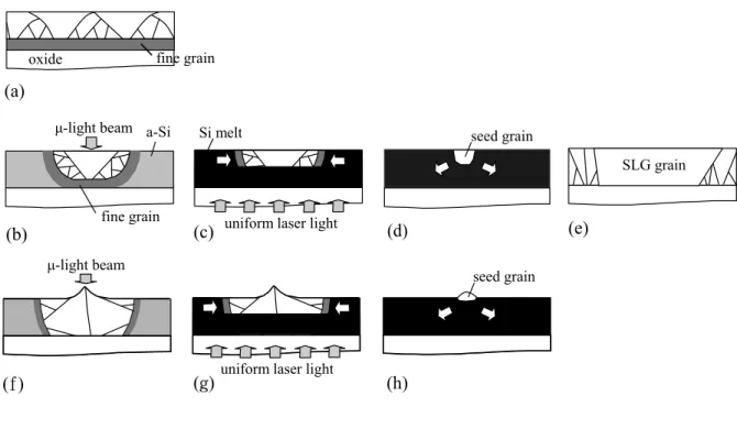
It has been elucidated that during the ELA of Si thin films,5-8) the melting and recrystallization dynamics vary with the excimer laser energy density. A cross-sectional diagram of Si film after excimer laser crystallization under partial melting, based on ref.8,8) is shown in Fig. 1(a). A certain thickness of the 20~50 nm fine sized crystalline layer formed by explosive crystallization (EC) remains at the substrate interface and then there is epitaxial growth from these EC grains toward the molten Si above it. During the epitaxial growth, grain regrowth involving the selection and widening of the favored grains occurs, and therefore, the grain size observed on the surface is larger than that of the EC crystallites. It is known that a grain growing in a supercooling melt releases latent heat, raising the surrounding temperature. This suppresses the growth of other grains. The partially melted Si film induced by laser irradiation is in a highly supercooling state7); thus, the selection and widening of the favored grains appears to be caused by such a mechanism. The growth of grains within the heat diffusion length from a prior grain is disturbed, and therefore, the radius of grains reflects the heat diffusion length to some degree.
The method proposed in this letter is based upon such an idea; that is, if the size of the supercooled melt is smaller than the heat diffusion length [Fig. 1(b)], then only one comparatively large grain can be formed within the melt. The diffusion length is comparable to the radius of the grain size under partial melting, on the bases of the above-mentioned assumption.
That is, approximately 0.4 μm for a 100 nm-thick Si layer at 550 oC9). The micromelt is formed by irradiation from a microlight beam (μ-light beam). For the formation of the μ-light beam, we propose a microlens array (MLA) to focus the excimer laser light. We call the above process the preseeding process. A seed region composed of one large central grain and surrounding small grains can be formed [Fig. 1(b)]. The film is then remelted with an opportune laser energy density to completely melt the a-Si, while keeping the poly-Si partially melted[Fig. 1(c)]. This is not difficult to achieve because of the difference in critical laser energy for complete melting between a-Si and crystalline Si6). Note that in this process the laser light was irradiated from underneath the substrate combined with light absorptive under layer in order to increase the distance of grain growth10). Therefore, the seed region at the substrate interface should be molten after the laser irradiation. When the laser energy density is higher than the threshold energy density for complete melting, the temperature of the Si melt exceeds its melting point. On the other hand, the temperature of the melt beneath the seed region is less than or equal to the melting point. As a result, the seed region continues melting laterally from its sides [as shown by the horizontal arrows in Fig1 (c)] even after laser irradiation, and therefore, the size of the seed region shrinks.
Hence, if there is a central large grain in the seed region, it is possible to produce a situation such as that in Fig. 1(d), where one grain remains among the Si melt pool. Then SLG of the grain originating at the residual grain can occur [Fig. 1(e)]. We call this the postgrowth process.
The sample preparation is as follows. An 800-nm-thick SiOxNy light absorptive underlayer with an absorption coefficient of 9000 cm-1 and a 100-nm-thick SiO2 buffer layer were deposited successively at 250 oC on a glass substrate by plasma-enhanced chemical vapor deposition (PECVD; hand-built) using Si(CH3)4 as the raw material. Then, 90-nm-thick Si was deposited at 200 oC by DC Ar sputtering (hand-built). The MLA was fabricated by the reflow method. A
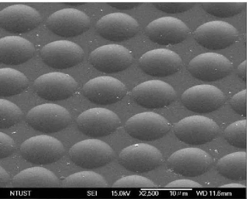
4.5-μm-thick photoresist (PR) on quartz was patterned in circles with a diameter of 8 μm and was reflowed at 160 oC for 5 min to form hemispherical PR patterns. Then, the PR together with underneath quartz was etched anisotropically. This process was carried out by reactive ion etching (RIE: hand-built) using CF4 and O2. Figure 2 shows a scanning electron microscopy (SEM) image of the MLA. The period of the microlens was 10 μm. The focus of the microlens was obtained experimentally to be 50 μm.
In the preseeding process, MLA was placed on the top surface of the Si film at an interval of 50 μm, its focal length, and then single pulse of a XeF excimer laser (Lambda-physik Compex102, 351 nm, 25 ns) with raw energy densities of 13~24 mJ/cm2, was irradiated onto the Si film at 500 oC from the top surface of Si film through the MLA. The raw laser energy density at a point in front of the MLA was measured by a joule meter. In the following postgrowth process, a single pulse of a uniformly distributed excimer laser (350 mJ/cm2) from the underneath of the substrate at 500 oC in atmosphere was used to completely melt the film. The Si films were then observed using SEM. Before SEM observation, the Si film was Secco-etched (50 % HF :H2O :CrO3 = 200 cc :100 cc :1.5 g) for 4 s.
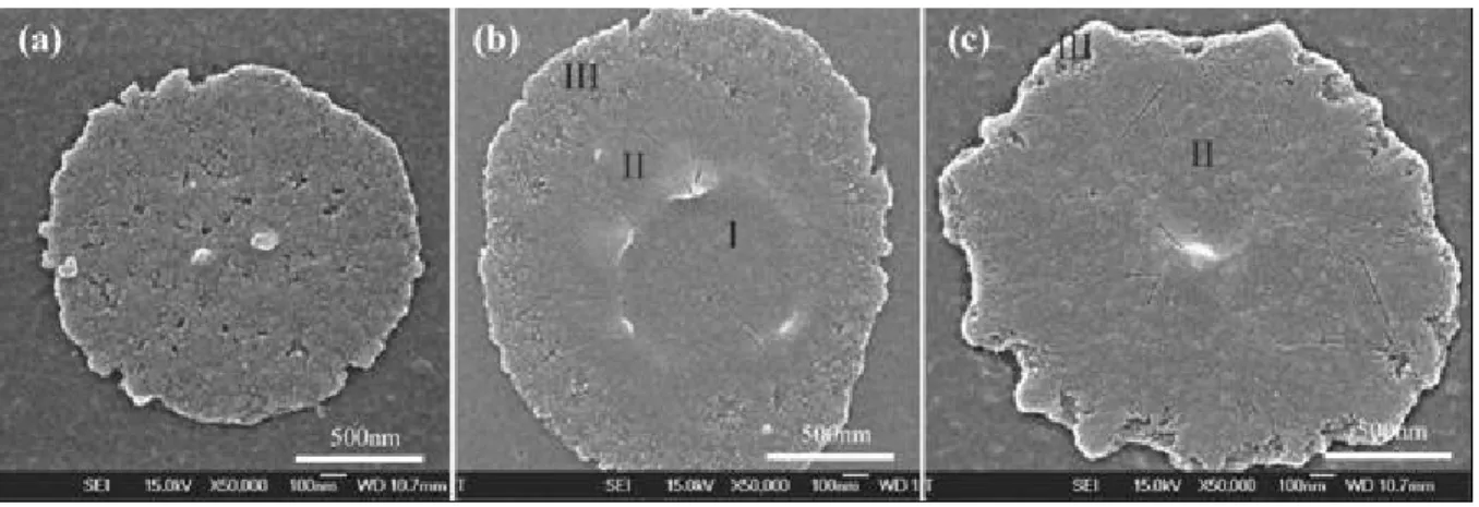
Figure 3 shows the seed regions formed after μ-light beam irradiation in the preseeding process with raw laser energy densities of 18, 21, and 24 mJ/cm2. At 18 mJ/cm2 [Fig. 3(a)], the spot is composed of only fine grains. This appearance, except for the change in spot size, did not change with decreasing energy density, until the spot disappeared at 13 mJ/cm2. Therefore, this seed region was caused by EC that occurs at energies larger than that required for surface melting.
At 21 mJ/cm2 [Fig. 3(b)], a comparatively large grain was formed at the center of the spot (region I). This grain is initially surrounded by lateral grains (region II) and then by fine grains in the outer part (region III). The scenario is as follows [Fig. 1(b)]: The μ-light beam caused partial melting at the center, and growth of the grains from surrounding EC grains at the side and the bottom of the melt occurred soon after laser irradiation. Because the size of the melt is comparable to twice of the heat diffusion length, a large grain can grow within the melt. Lateral grains (region II) also originated from region III grew inward and then impinged on the large central grain. At 24 mJ/cm2 [Fig. 3(c)], only regions II and III are present. This appearance does not change with increasing laser energy density until ablation occurs at the center of the spot.
Therefore, Fig. 3(c) shows a complete melting condition. Hence growth of grains does not originate from underneath of the melt but only from outer part of the melt (region III), and grains grow laterally into the central melt, and then impinge on each other at the center of the seed region. The cross section of the seed region was presumed to be as that shown in Fig. 1(f).
Impingements of grains result in a protrusion at the center of the seed region owing to the mismatch of densities between solid and liquid of silicon11).
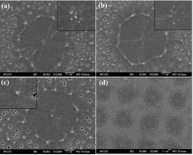
Figure 4 shows the SLG grains after postgrowth with different preseeding energy densities.
The insert show the magnified images of the center of the SLG grain. At a seeding energy of 18 mJ/cm2 [Fig. 4(a)], grains grew radially from the seed region and can be considered to be multiple grains. This occurred because the grain size is uniform, and therefore, more than one grain remained during postgrowth. At a seeding energy of 21 mJ/cm2 [Fig. 4(b)], the SLG grain is a single grain. Some protrusions can be seen at the seed region; however, these protrusions seem to have no influence on single-grain growth. This result is consistent with the scenario shown in Figs. 1(b)-1(e). At 24 mJ/cm2 [Fig. 4(c)], the SLG grain is also a single grain. The scenario is as
follows. During postgrowth, the seed region was remelted from the side (Fig. 1(g)). During remelting, the center protrusion is more difficult to be melted because of its larger cross section of solid. Thus, the protrusion remains in the Si melt pool [Fig. 1(h)]. Then, an SLG single grain originates from this protrusion. Figure 4(d) shows a grid of SLG grains. SLG grains can be localized precisely.
In conclusion in this letter, we presented a method of controlling the location of crystal grains by ELA of Si thin films. A local area of the Si film was melted by a micro light beam, and one comparatively large grain was formed in the melt when the film was under a partially melted condition. In a successive process, Si was remelted, and the comparatively large grain induced the SLG grain. As a result, location-controlled SLG grains with a diameter of 6 μm were formed.
Such a grain location control method provides a basis for the fabrication of single-grain TFTs, which are essential for the device–to–device uniformity of high-performance TFTs.
References
1. J. S. Im, R. S. Sposili and M. A. Crowder: Appl. Phys. Lett. 70 (1997) 3434.
2. M. Nakata, K. Inoue and M. Matsumura : Jpn. J. Appl. Phys. 40 (2001) 3049.
3. P. C. van der Wilt, B. D. van Dijk, G. J. Bertens, R. Ishihara and C. I. M. Beenakker: Appl.
Phys. Lett. 72 (2001) 1819.
4. H. Kumomi: Appl. Phys. Lett. 83 (2003) 434.
5. J. S. Im, H. J. Kim and M. O. Thompson: Appl. Phys. Lett. 63 (1993) 1969.
6. M. Hatano, S. Moon, M. Lee, K. Suzuki and C. P. Grigoropoulos: J. Appl. Phys. 87 (2000) 36.
7. M. Hatano, S. Moon, M. Lee, K. Suzuki and C. P. Grigoropoulos: Mater. Res. Soc. Symp.
Proc. 558 (2000) 193.
8. F. C. Voogt, R. Ishihara and F. D. Tichelaar: J. Appl. Phys. 95 (2004) 2873.
9. J. S. Im, H. J. Kim and M. O. Thompson: Appl. Phys. Lett., 63 (1993) 1969.
10. W. C. Yeh: Dig. Tech. Pap. Active Matrix Liquid Crystal Display 2002, J. Soc. Appl. Phys., 2002, p. 153.
11. D. Pribat, P. Legagneux, F. Plais, C. Reita, F. Petinot and O. Huet: Mater. Res. Soc. Symp.
Proc. 424 (1997) p.127.
Figure Captions
Fig. 1 Schematic diagrams of cross sections of (a) grain growth under partially melting condition.
(b) Grain growth in micromelt under partial melting condition induced by μ-light beam.
(c) Remelting of film by laser irradiation from underneath. Horizontal arrows show the directions of successive melting. (d) Grain growth from seed grain. Horizontal arrows show the directions of grain growth. (e) SLG grain originating from seed grain. (f) Grain growth in micromelt under complete melting condition induced by μ-light beam. (g) Remelting of film by laser irradiation from underneath. Horizontal arrows show the directions of successive melting. (h) Grain growth from seed grain. Arrows show the directions of grain growth.
Fig. 2 SEM image of microlens array.
Fig. 3 SEM images of seed region formed after μ-light beam irradiation with raw energy densities of (a) 18, (b) 21 and (c) 24 mJ/cm2 in preseeding process.
Fig. 4 SEM images of location-controlled SLG grains with different preseeding raw energy density of (a) 18, (b) 21 and (c) 24 mJ/cm2. The inserts are the zoomed pictures of the center of the SLG grain. (d) Array of SLG grains.
SLG grain oxide
fine grain
a-Si Si melt seed grain
seed grain fine grain
μ-light beam
μ-light beam
uniform laser light
(a)
(b) (c)
(h)
(d) (e)
oxide
(f)
oxide oxide
(g) uniform laser light