Shou Chang Cheng and Kwang Lung Lin
Department of Materials Science and Engineering, National Cheng-Kung University, Tainan, Taiwan 701, Republic of China
(Received 6 November 2002; accepted 6 May 2003)
The interfacial intermetallic formation at 150 °C between Cu and various solders, including Sn–9Zn, Sn–8.55Zn–1Ag, and Sn–8.55Zn–1Ag–XAl was investigated. The Al contents X of the quaternary solder alloys investigated were 0.01–0.45 wt.%. The compositions and the growth kinetics of intermetallic compounds (IMCs) were investigated. The IMC consisted of three layers for Sn–9Zn/Cu, Sn–Zn–Ag/Cu, and Sn–Zn–Ag–XAl/Cu specimens after aging for 100–600 h. These three layers included the Cu3(Zn,Sn) phase adjacent to the solder, the Cu6(Sn,Zn)5phase in the middle,
and the Cu-rich phase near to Cu. For long-term aging time over 1000 h, the Cu6(Sn,Zn)5phase grew, while the Cu3(Zn,Sn) phase diminished. Al segregation
formed in the IMC for all of the Sn–Zn–Ag–XAl/Cu specimens after aging.
Cracks formed, when aged for 1000 h, at the solder/IMC interface or within the IMC layer for the following solders: Sn–9Zn, Sn–8.55Zn–1Ag, Sn–8.55Zn–1Ag–0.1Al, Sn–8.55Zn–1Ag–0.25Al, and Sn–8.55Zn–1Ag–0.45Al. The crack was not detected up to 3000 h for the Sn–8.55Zn–1Ag–0.01Al/Cu couple, of which the IMC growth rate was the slowest among all solders.
I. INTRODUCTION
Pb-free solder has been an important issue in elec-tronic material development for a decade. Many Sn-based ternary and quaternary Pb-free systems have been investigated.1–9 A drop-in replacement lead-free solder alloy has to satisfactorily address melting temperature, wettability, electrical and thermal conductivity, thermal expansion coefficient, mechanical strength and ductility, creep resistance, thermal fatigue resistance, corrosion re-sistance, and manufacturability.5
Therefore an acceptable Pb-free alternative for Sn–Pb solder should be superior or equivalent to Sn–Pb solder in the above-mentioned properties. This is crucial in applications, for instance, in avionics and automotive where solder is subjected to thermal cycles and high temperature circumstances up to 150 °C.10 The formation of intermetallic compounds (IMCs) will affect the reliability of solder joint.
IMC layers including Cu6Sn5 next to solder and
Cu3Sn next to Cu pad are observed in all aged Sn–Ag/Cu
and Sn–Pb–Ag/Cu solder joints. The Ag3Sn particles in
Sn–Ag solder grow slowly during the aging process.11 The Cu5Zn8 IMC layer was observed at the interface
between the Sn–XZn (X ⳱ 3, 6, and 9 wt.%) solder and Cu rod when soldered at 290 °C.12 Transmis-sion electron microscopy analysis shows that the Sn– 3.6Pb–2Ag/Pd–3Ag/Al2O3 system forms a variety of
IMC phases near the substrate after aging at 150 °C for
32 days.13 These IMCs include Ag5Sn, Ag3Sn, Pd2Sn,
PdSn2, PdSn4, Pd3Sn2, PdSn, PbPd3, and Pd3Pb5.
Formation of the multiphase IMC layer is the main factor that affects reliability of surface mounted thick film solder joints on ceramic substrate.13 The thickness of the IMC was largest for Sn–3.5Ag–6.5In among the Sn3.5Ag–X (X ⳱ Cu, In, and Ni)/Au/Ni/Cu system, irrespective of soldering (250 °C for 60 s), aging (130 °C for 100 h), and thermal cycling (−65 to 150 °C for 100 cycles) conditions. The Cu6Sn5particles seemed
to attach to the interfacial IMC for the Sn–3.5Ag–1.5Cu solder.14
The IMCs formed between eutectic Sn–Pb, Sn–3.5Ag, Sn–3.8Ag–0.7Cu, and Sn–0.7Cu solders and Cu were studied for aging at 125, 150, and 170 °C.15The growth rate of IMCs in eutectic Sn–Pb is faster than that in Pb-free solders and the same type of IMCs (Cu6Sn5
and Cu3Sn) are formed in all the solders.
Wettability is the base to all soldering processes. It is of importance to understand the thermodynamics and ki-netics of wetting interaction between solder and sub-strate. The present study investigated the interfacial interaction during soldering of Cu by Sn–Zn–Ag–Al sol-ders. Investigations focused on the microstructure and growth of IMC formed between Cu and Sn–Zn–Ag–Al solders for aging at 150 °C. The effect of Al element on microstructure and IMC growth between the solder and copper were also investigated in this work.
II. EXPERIMENTAL
A 99.9% pure copper rod with 1-mm diameter was applied as the substrate for wetting investigation. The specimen was sequentially degreased in 5 wt.% NaOH at 70 °C for 5 min, rinsed in deionized (DI) water for 5 s, cleaned in 10 vol% HNO3 for 5 s, rinsed in DI
water for 5 s, and finally cleaned with 98% alcohol so-lution for 5 s, and dried. After the pretreatment, the speci-men was dipped in the dimethylammonium chloride flux (2.5 g/100 ml C2H5OH) for 30 s. Preheating was
con-ducted at 60 °C for 20 s to avoid formation of bubbles at the interface between solder and Cu substrate. The solders investigated include eutectic Sn–9Zn and Sn–8.55Zn–1Ag–XAl (X ⳱ 0, 0.01, 0.1, 0.25, and 0.45 wt.%) solders. The Sn–8.55Zn–1Ag–XAl solders show less dross formation than Sn–9Zn and Sn–8.55Zn– 1Ag solders. The wetting investigation was conducted with wetting balance. The investigation was performed at 250 °C with an immersion time of 15 s, immersion depth of 9.9 mm, and immersion speed of 15 mm/s. The sol-dered specimens were then aged in oven at 150 °C for 100–3000 h. The cross-sectional microstructure of the soldered specimens was etched in a 0.2 vol% HCl solu-tion prior to investigasolu-tion with scanning electron micros-copy (SEM), energy dispersive spectrosmicros-copy (EDS), and electron probe microanalysis (EPMA).
III. RESULTS
A. Microstructural analyses 1. Eutectic Sn–9Zn solder
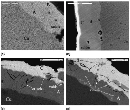
Figure 1 shows the interfacial microstructures formed between Sn–9Zn solder and Cu substrate after aging at 150 °C for 100, 300, and 1000 h. The IMC layer formed in the Sn–9Zn/Cu specimen after aging at 150 °C for 100 h is not visible with backscattering electron imaging (BEI). The results of EDS analysis (Table I) show that compositions of points A and B of Fig. 1(a) in the solder matrix are Cu3(Zn,Sn) and Cu6(Sn,Zn)5phases. Further
aging up to 300 h gives rise to Cu-rich, Cu3(Zn,Sn) and
Cu6(Sn,Zn)5phases, as shown respectively for points A,
B, and C in Fig. 1(b). Further aging up to 1000 h resulted in voids and cracks appearing within the interfacial re-gion of the Sn–9Zn/Cu specimen [Figs. 1(c) and 1(d)]. The analysis shows the existence of Cu-rich phase [Sn4Zn13Cu84, point A of Fig. 1(c)] next to the Cu
sub-strate. The IMC compounds formed (Table I) are also Cu3(Zn,Sn) (Sn18Zn19Cu63of point B) and Cu6(Sn,Zn)5
(Sn38Zn8Cu55 of point C) phases.
2. Sn–8.55Zn–1Ag solder
The as-soldered Sn–8.55Zn–1Ag/Cu specimen forms a compound layer at the interface. Figure 2(a) shows a cross-sectional view of microstructure for the Sn–8.55Zn–1Ag/
FIG. 1. Cross-sectional views of microstructure of the eutectic Sn–9Zn solder/Cu interface, after aging for (a) 1000 h (BEI), (b) 300 h (SEM), and (c,d) 1000 h (BEI), present different areas of a specimen.
Cu specimen after aging at 150 °C for 600 h. The aging process gives rise to various compositions (Table I) in the specimen as Cu-rich [point A of Fig. 2(a), Sn3Zn7Cu90],
Cu3(Zn,Sn) [point B of Fig. 2(a), Sn16Zn24Cu60], and
Cu6(Sn,Zn)5 [point C of Fig. 2(a), Sn34Zn9Cu57]. After
1700 h [Fig. 2(b)], the compositions (Table I) detected are Cu3(Zn,Sn) (point A, Sn28Zn4Cu67) and Cu6(Sn,Zn)5
(point B, Sn41Zn6Cu52). Further aging up to 1700 h
re-sulted in the appearance of voids and cracks within the interfacial region of the Sn–8.55Zn–1Ag/Cu specimen [Fig. 2(b)]. It is very interesting that Ag–Zn compounds are dissolved after the aging process. The Ag contents of
all the analyzed positions for both IMC and solder are within 1 at.%. No Ag segregation or Ag compound formed with the other elements.
3. Sn–8.55Zn–1Ag–XAl solder (X = 0.01, 0.1, 0.25, and 0.45 wt.%)
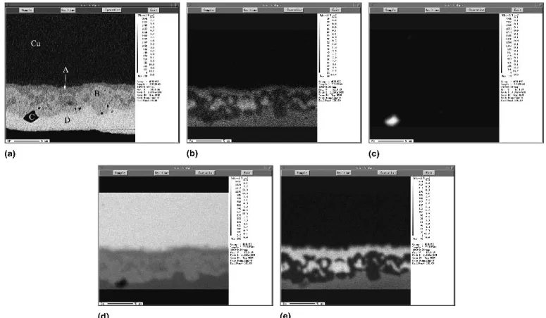
The BEI image in Fig. 3(a) clearly differentiates the various phases formed within the 0.01 Al-containing sol-der. It is noticed that Al will segregate (point C) as char-acterized in Fig. 3(c). The segregation of Al has also been detected for Sn–Zn–Al system.3 Ag shows strong asso-ciation with Zn as evidenced by the EPMA analysis
TABLE I. Compositions of the IMC formed at the solder/Cu interface after aging at 150 °C for different aging time. Solders are Sn–9Zn, Sn–8.55Zn–1Ag, Sn–8.55Zn–1Ag–XAl.
Solders Aging time (h) IMC compositions Note
Sn-9Zn 100 Cu3(Zn,Sn) Fig. 1(a): Point A
Cu6(Sn,Zn)5 Point B
300 Cu-rich(67 at.%) Fig. 1(b): Point A
Cu3(Zn,Sn) Point B
Cu3(Sn,Zn)5 Point C
1000 Cu-rich(84 at.%) Fig. 1(c), (d): Point A
Cu3(Zn,Sn) Point B
Cu6(Sn,Zn)5 Point C
Sn-8.55Zn-1Ag 600 Cu-rich(90 at.%) Fig. 2(a): Point A
Cu3(Zn,Sn) Point B
Cu6(Sn,Zn)5 Point C
1700 Cu-rich(67 at.%) Fig. 2(b): Point A
Cu6(Sn,Zn)5 Point B
Sn-8.55Zn-1Ag-0.01Al 1000 Cu-rich(67 at.%) Fig. 3(a): Point A
Al–Cu compound Point B
Al–Cu compound Point C
Cu6(Sn,Zn)5 Point D
Sn-8.55Zn-1Ag-0.1Al 300 Cu3(Zn,Sn) Fig. 4(a): Point A
Cu6(Sn,Zn)5 Point B
Al–Cu compound Point C
600 Cu3(Zn,Sn) Fig. 4(b): Point A
Cu6(Sn,Zn)5 Point B
Al–Cu compound Point C
1000 Cu6(Sn,Zn)5 Fig. 4(c): Point A
Al–Cu compound Point B
1700 Cu6(Sn,Zn)5 Fig. 4(d): Point A
Al–Cu compound Point B
Sn-8.55Zn-1Ag-0.25Al 300 Cu-rich(69 at.%) Fig. 5(b): Point A
Al–Cu compound Point B
Al–Cu compound Point C
Cu6(Sn,Zn)5 Point D
600 Cu-rich(71 at.%) Fig. 5(c): Point A
Cu6(Sn,Zn)5 Point B
Al–Cu compound Point C
Cu6(Sn,Zn)5 Point D
1000 Cu3(Zn,Sn) Fig. 5(e): Point A
Cu6(Zn,Sn)5 Point B
Al–Cu compound Point C
Cu6(Sn,Zn)5 Point D
Sn-8.55Zn-1Ag-0.45Al 300 Cu6(Sn,Zn)5 Fig. 6(a): Point A
Al–Cu compound Point B
Al–Cu compound Point C
600 Cu-rich(71 at.%) Fig. 6(b): Point A
[Figs. 3(b) and 3(e)]. However, the compositional analysis at points A, B, and C was unable to detect Ag (Table I). This further indicates that Ag is not engaged in the Sn–Zn–Cu compounds. Aging of higher Al wt.% speci-mens, Sn–8.55Zn–1Ag–(0.1–0.45) wt.% Al (Figs. 4–6), produced cracks at the interface between IMC and solder. The IMC layer consists of Sn-Zn-Cu as presented
in Table I. It is also noticed that Al tends to segregate at the interface between solder and IMC upon aging as evidenced by the result of Table I and Fig. 7(c). The increase in Al content destroys the affiliation between Ag and Zn [Figs. 7(b) and 7(e)], compared to the occurrence in 0.01 wt.% Al-containing solder [Figs. 3(b) and 3(e)]. This phenomenon is further observed after aging for
FIG. 2. Cross-sectional view of microstructure for the Sn–8.55Zn–1Ag solder/Cu substrate after aging for (a) 600 h (BEI) and (b) 1700 h (SEM) at 150 °C.
FIG. 3. Microstructure and EPMA analysis of Sn–8.55Zn–1Ag–0.01Al solder after aging at 150 °C for 1000 h. (a) BEI and elemental analysis of (b) Ag, (c) Al, (d) Cu, and (e) Zn.
1700 h (Fig. 8). Both Al and Ag were seen to move to the interface between solder and IMC [Fig. 8(b)] or even to the outer solder layer [Fig. 8(c)]. A further increase in Al content up to 0.25 wt.% (Fig. 5) and 0.45 wt.% (Fig. 6) shows segregation of Al as evidenced by the elemental analysis (Table I) of all point Cs of these two specimens.
B. Thermodynamic of IMC growth
It was described earlier that the IMC layer grows upon aging at 150 °C. The growth behavior of the IMC layer with respect to the square root of time (Fig. 9) shows a linear correlation for all solders. This result shows that the formation of the IMC for all investigated solders is a diffusion-controlled process. The rate constants for the Sn–9Zn and Sn–Zn–1Ag solders are closing to each other, indicating the same IMC formation reaction. It is of interest to notice that the small addition of 0.01 wt.% Al greatly lowers the rate constant. The 0.01 wt.% Al-containing solder exhibits the smallest rate constant. In other words, the addition of Al to 0.01 wt.% prominently lowers the formation rate of the IMC. The degradation
effect exists up to 0.1 wt.% Al. The greatest growth rate of IMC occurs for the Sn–8.55Zn–1Ag–0.25Al/Cu speci-mens, followed by the Sn–8.55Zn–1Ag–0.45Al/Cu specimens.
IV. DISCUSSION
1. Eutectic Sn–9Zn solder
The IMC was found to consist of three layers for the as-soldered Sn-9Zn/Cu specimen.12,16These three layers include the␥–Cu5Zn8adjacent to the solder, the–CuZn
in the middle, and the unknown thinnest layer near to Cu. All these layers do not contain Sn.16These Cu–Zn layers are not stable and may further react with Cu to form Cu5Zn8particulate after aging at 150 °C for 100 h. Sn
may also easily diffuse through the IMC layer to form the Cu6Sn5.
16
Thus, Cu–Zn compounds form and Cu6Sn5is
scattered within the IMC layer after aging at 150 °C. Thermodynamically, the Gibbs free energy of a IMC formation reaction must be a negative value to form the
FIG. 4. Cross-sectional microstructure of the Sn–8.55Zn–1Ag–0.1Al solder/Cu specimen after aging for (a) 300 h, (b) 600 h, (c) 1000 h, and (d) 1700 h.
referred IMC. The Gibbs free energy of formation for Cu–Sn compound is⌬G150 °C⳱ −4.255 to −6.255 KJ/mol, and that for the Cu–Zn compound is −4.715 to −8.355 KJ/mol.17
Yet, the reaction between Sn and Zn exhibits a positive value (⌬G150 °C ⳱ 0.163 to
3.866 KJ/mol) of Gibbs free energy.17,18
Accordingly, the compound layer is composed of the mixture of Cu–Sn and Cu–Zn compounds. The Sn12Zn22Cu66
com-position [Fig. 1(a), point A] is regarded as representing
the Cu3(Zn,Sn) compound belonging to the Cu3Zn phase.
Meanwhile, the composition Sn27Zn15Cu59 [Fig. 1(a),
point B] seems to be the Cu6(Sn,Zn)5 compound that
belongs to the Cu6Sn5 phase. Nevertheless, a
compari-son between Figs. 1(a) and 1(c) reveals that the layer A of Fig. 1(c) was not observed after aging for 100 h [Fig. 1(a)]. Accordingly, solid-state aging significantly varies the formation of IMC. Further aging up to 1000 h resulted in the formation of voids and cracks within the
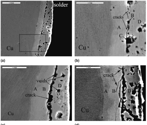
FIG. 5. Cross-sectional microstructure of the Sn–8.55Zn–1Ag–0.25Al/Cu specimen after aging at 150 °C for (a) 300 h, (b) enlargement of inset of (a), (c) 600 h (SEM), and (d) 1000 h (SEM).
FIG. 7. Cross-sectional microstructure and EPMA analysis of Sn–8.55Zn–1Ag–0.1Al/Cu specimen after aging at 150 °C for 300 h. (a) BEI and elemental analysis of (b) Ag, (c) Al, (d) Cu, and (e) Zn.
FIG. 8. Cross-sectional microstructure and EPMA analysis of Sn–8.55Zn–1Ag–0.1Al/Cu specimen after aging at 150 °C for 1700 h. (a) BEI and elemental analysis of (b) Ag, (c) Al, (d) Cu, and (e) Zn.
interfacial region of the Sn–9Zn/Cu specimen [Figs. 1(c) and 1(d)]. The voids are believed to be the Kirkendall voids formed as a result of counterdiffusion between Cu and Sn.19,20Combination of voids may give rise to cracks upon extended aging. Nevertheless, it is also likely that the stress induced by the IMC growth results in crack formation. Most of the cracks are not parallel to the interface and, apparently, are not associated with Kirkendall voids.
2. Sn–8.55Zn–1Ag solder
It was found that the Ag–Zn compounds are dissolved after the aging process. There was not detected any Ag segregation or formation of Ag compound with the other elements. The observations are explained as fol-lows. The Sn–Zn binary phase diagram18 indicates that Ag exhibits 1 at.% solid solubility in Zn while zero solubility in Sn.15 The Gibbs free energies for the for-mation of various compounds at 150 °C are −4.263 to −4.824 KJ/mol (AgZn3), −2.320 KJ/mol (⑀–Ag3Sn),
−4.255 to −5.179 KJ/mol (–Cu6Sn5), −8.042 to
−8.335 KJ/mol (␥–Cu5Zn8), and −4.715 to −6.197 KJ/mol
(–CuZn).17
Hence, the relative sequence of the forma-tion of these compounds is ␥–Cu5Zn8 > –CuZn >
–Cu6Sn5 ∼ AgZn3 > ⑀–Ag3Sn under solid state. This
information provides an explanation why Ag–Zn com-pound was not observed. Thus, it is difficult to form Ag–Zn and Ag–Sn compounds compared to Cu–Zn and Cu–Sn compounds, according to the magnitude of the Gibbs free energy. The Ag–Zn binary phase diagram21 indicates that Ag exhibits 1 at.% solid solubility in Zn
and zero solubility in Sn. According, Zn preferentially forms the Cu–Zn compound. Further aging up to 1700 h resulted in the appearance of voids and cracks within the interfacial region of the Sn–8.55Zn–1Ag/Cu specimen [Fig. 2(b)]. The cracks, existing parallel to the interface between IMC and solder, are believed to result partly from the merging of Kirkendall voids.
3. Sn–8.55Zn–1Ag–XAl solder (X = 0.01, 0.1, 0.25, and 0.45 wt.%)
Al tends to segregate at the interface between solder and IMC upon aging as evidenced by the results given in Table I and Fig. 7(c). The increase in Al content destroys the affiliation between Ag and Zn [Figs. 7(b) and 7(e)], compared to the occurrence in 0.01 wt.% Al-containing solder [Figs. 3(b) and 3(e)]. This phenomenon is further observed after aging for 1700 h (Fig. 8). The interaction between Cu and Al may form the␥–Cu9Al4 compound
of which the Gibbs free energy of formation is −12.053 KJ/mol.17
The absolute value of this Gibbs free energy is greater than that of the Cu–Sn and Cu–Zn compounds. Accordingly, Cu tends to react with Al rather than with Zn or Sn when coexisting with these elements as delineated by the composition analysis (Table I). The Cu–Al compound shows no solubility with the Cu–Sn or Cu–Zn compound and thus is “expelled” to the interface between the Sn–Zn–Cu compound layer and the outer unreacted solder layer. Similarly, Ag also shows strong association with Zn as evidenced by the EPMA analysis in Figs. 3(b) and 3(e). Aging of the higher Al wt.% specimen, Sn–8.55Zn–1Ag–(0.1–0.45)Al (Figs. 4–6), produced cracks at the interface between the IMC and solder. This phenomenon is also likely to be ascribed to the combination of Kirkendall voids and the stress induced by the IMC growth.
It is also noticed that the solder layer contains high Cu content in all analyzed area for all the solders/Cu speci-mens. The Cu content is believed to diffuse to the solder from substrate during the wetting and aging process. Liquid-state diffusion is much faster than solid-state dif-fusion. For instance, it may take 1000 h of solid-state aging to form a certain thickness of IMC that would form during a wetting process for a few minutes.11,20,22–30
B. Thermodynamic of IMC growth
The addition of Al lowers the formation rate of the IMC. The behavior lasts at Al addition from 0.01 to 0.1 wt.%. The major IMCs formed in the specimen are Cu–Sn and Cu–Zn compounds. Of these elements—Al, Sn, and Zn—Cu will preferentially form a compound with Al over the others. Thus, the addition of Al will compete for Cu to form a Cu–Al compound. The barrier effect of this Cu–Al compound on counterdiffusion between Cu and solder was reported for the Sn–Zn–Al solder in contact
FIG. 9. Growth of total intermetallic compound with respect to the (aging time)1/2for different solder/Cu specimens.
with Cu.31It is believed that the decrease in growth rate (Fig. 9) of the IMC layer in 0.01–0.1 wt.% Al-containing solder results from the barrier effect. The barrier effect, however, diminishes at further addition of Al. It is evi-dent that the IMC layer exhibits cracks and voids upon aging for the higher Al content solder (Figs. 4–6). The barrier effect was thus destroyed and higher IMC growth rates were achieved for 0.25 wt.% and 0.45 wt.% Al-containing solders.
Additionally, Al tends to form a Cu–Al compound. Al competes against Zn for Cu, but has no chemical reaction with Sn. Al may form a Ag–Al compound; yet the opportunity of the Ag–Al compound formation decreases with the formation of the stable Ag–Zn compound.19 Therefore, increasing the addition of Al within 0.01–0.1 wt.% is helpful for lowering the growth rate of IMC for the Sn–8.55Zn–1Ag–XAl solder/Cu specimen. The results of Fig. 9 further reveal a minimum in IMC formation rate at 0.01 wt.% Al. In view of the cracks and voids observed at higher Al content (0.25 wt.% Al and 0.45 wt.% Al), it is suspected that extensive forma-tion of Cu–Al compound will degrade the compactness of the compound layer. In other words, a thin Cu–Al compound layer may give rise to a dense compact struc-ture and thus a satisfactory barrier effect. An increasing Al content may produce undesired structure as far as diffusion barrier is concerned. Nevertheless, all of the hypotheses need further experimental approval.
V. CONCLUSION
The IMCs produced upon aging of Cu/Sn–XZn–YAg– XAl specimens are mainly formed among Cu, Zn, and Sn. The growth of IMC layer is a diffusion-controlled process. Extending aging at 150 °C of the Cu/Sn–9Zn, Cu/Sn–8.55Zn–1Ag, and Cu/Sn–8.55Zn–1Ag–XAl specimens resulted in formation of cracks and voids at IMCs/solders interface as well as in the IMC layer. Sn– 8.55Zn–1Ag–0.01Al/Cu is the only specimen that shows no cracks upon aging. Cu may also form a compound with Al. The Cu–Al compound exists between the major IMC layer and solder and acts as the barrier layer to counter diffusion between Cu and other solder elements. The 0.01–0.1 wt.% Al-containing solders exhibit a lower IMC growth rate than Sn–9Zn and Sn–8.55Zn–1Ag sol-ders; yet, a further increase of Al content will raise the growth rate.
ACKNOWLEDGMENT
The financial support of this work from National Sci-ence Council of the Republic of China under Project No. NSC-90-2216-E-006-052 is gratefully acknowledged.
REFERENCES
1. F.G. Yost, in The Metal Science of Joining, edited by M.J. Cieslak, J.H. Perepezko, S. Kang, and M.E. Glicksman (TMS, Warrendale, PA, 1992), p. 49.
2. M. McCormack, S. Jin, and H.S. Chen, J. Electron. Mater. 23, 687 (1994).
3. K.L. Lin, L.H. Wen, and T.P. Liu, J. Electron. Mater. 27, 97 (1998).
4. K.L. Lin and T.P. Liu, Mater. Chem. Phy. 56, 171 (1998). 5. M. Yamashita, S. Tada, and K. Shiokawa, United States Patent
No. US006156132A, Dec. 5, 2000.
6. H. Mavoori, J. Chin, S. Vaynman, B. Moran, L. Keer, and M. Fine. J. Electron. Mater. 26, (1997).
7. S.P. Yu, M.H. Hon, and M.C. Wang, J. Electron. Mater. 16, 76 (2001).
8. Z. Mei and J.M. Morris, Jr., J. Electron. Mater. 21, 599 (1992). 9. W.J. Plumbridge, J. Mater. Sci. 31, 2501 (1996).
10. S. Ahat, M. Sheng, and L. Luo, J. Electron. Mater. 30, 1317 (1999).
11. K. Suganuma, K. Niihara, T. Shoutoku, and Y. Nakamura, J. Mater. Res. 13, 2859 (1998).
12. G.Y. Li, Mater. Sci. Eng. B 88, 47 (2002).
13. W.K. Choi, J.H. Kim, S.W. Teong, and H.M. Lee, J. Mater. Res.
17,43 (2002).
14. T.Y. Lee, W.J. Choi, and K.N. Tu, J.W. Jang, S.M. Kao, J.W. Jang, S.M. Kuo, J.K. Lin, D.R. Frear, K. Zeng, and J.K. Kivilahti, J. Mater. Res. 17, 291 (2002).
15. T.B. Massalski, J.L. Murray, L.H. Bennett, H. Baker, and L. Kacprzak, Binary Alloy Phase Diagram, 2nd ed. (ASM New York, 1987), pp. 70, 71.
16. K. Suganuma, T. Murata, H. Noguchi, and Y. Toyoda, J. Mater. Res. 15, 884 (2000).
17. R. Hultgren, P.D. Desai, D.T. Hawkins, M. Gleiser, and K.K. Kelley, Selected Values of Thermodynamic Properties of
Binary Alloys (ASM, Metals Park, OH, 1973), pp. 19, 1336.
18. T.B. Massalski, J.L. Murray, L.H. Bennett, H. Baker, and L. Kacprzak, Binary Alloy Phase Diagram, 2nd ed. (ASM New York, 1987), pp. 85, 86.
19. S. Ahat, M. Shang, and L. Luo, J. Mater. Res. 16, 2914 (2001). 20. W. Yang, R.W. Messler, Jr., and L.E. Felton, J. Electron. Mater.
23,765 (1994).
21. T.B. Massalski, J.L. Murray, L.H. Bennett, H. Baker, and L. Kacprzak, Binary Alloy Phase Diagram, 2nd ed. (ASM New York, 1987), pp. 2085, 2086.
22. K.N. Tu, T.Y. Lee, J.W. Jang, L. Li, D.R. Frear, K. Zeng, and J.K. Kivilahti, J. Appl. Phys. 89, 4849 (2001).
23. D.R. Flanders, E.G. Jacobs, and R.F. Pinizzotto, J. Electron. Mater. 26, 883 (1997).
24. S.W. Chen and Y.W. Yen, J. Electron. Mater. 28, 1203 (1999). 25. G. Careri and A. Paoletti, Nuovo Cimento 10, 575 (1958). 26. G. Careri, A. Paoletti, and M. Vincentini, Nuovo Cimento 10,
1088 (1958).
27. C.H. Ma and R.A. Swalin, J. Chem. Phys. 36, 3014 (1962). 28. Y.P. Gupta, Acta Metall. 14, 1007 (1966).
29. C.H. Ma and R.A. Swalin, Acta Metall. 8, 388 (1960). 30. G. Ghosh, Acta Mater. 49, 2609 (2001).