科技部補助專題研究計畫成果報告 期末報告
具高安全性且易於整合的車用類比至數位轉換器之研製(第2年)
計 畫 類 別 : 個別型計畫
計 畫 編 號 : MOST 105-2221-E-006-240-MY3 執 行 期 間 : 106年08月01日至107年07月31日 執 行 單 位 : 國立成功大學電機工程學系(所)
計 畫 主 持 人 : 張順志
計畫參與人員: 碩士班研究生-兼任助理:簡銘宏 碩士班研究生-兼任助理:簡豪廷 碩士班研究生-兼任助理:孔致遠 碩士班研究生-兼任助理:林育賢 碩士班研究生-兼任助理:胡家瑋 碩士班研究生-兼任助理:黃聖文 碩士班研究生-兼任助理:張力仁
報 告 附 件 : 出席國際學術會議心得報告
中 華 民 國 107 年 10 月 31 日
中 文 摘 要 : 本研究計畫的主要目標在研製契合汽車應之用高速低耗能的類比至 數位轉換器,其除了易於與感測器在高電壓系統中整合外,更著重 在研發不受環境干擾的穩定訊號轉換技術,以提升車用電子系統的 安全性。整個計畫可概分為三大研究子題:(1)易於與感測器在高電 壓系統中整合之類比至數位轉換器設計技術;(2)解決亞穩態之類比 至數位轉換器設計技術;(3)抗雜訊之類比至數位轉換器設計技術。
本計畫第一年將針對上述研究子題開發合適的架構與電路設計技術
,並著手研製雛型晶片。第二年的研究重點將著重於驗證雛型晶片
,進行架構調整與電路優化的設計,並研製完整的類比至數位轉換 器晶片。第三年的研究重點將放在整合量測驗證。
中 文 關 鍵 詞 : 類比至數位轉換器、汽車電子、雜訊、亞穩態、易於整合。
英 文 摘 要 : The main objectives of this project are to investigate and develop design techniques for high-speed low-energy
consumption analog-to-digital circuits (ADC), which are not only easily to be integrated with sensors in high-voltage environments, but also very stable during conversion even in noisy environments. The whole project is divided into three sub-topics: (1) design techniques for integrating with sensors in high-voltage environments; (2) design techniques for solving metastable problems during
conversion; and (3) design techniques for alleviating the effects sourced from noise. In the first year, we will develop proper structure and circuit design techniques for the abovementioned sub-topics. Several proof-of concept prototypes will be carried out during this stage. In the second year, we will focus on verifying the prototypes, refining the designs and type out the complete chips. In the last year, we will focus on the integration and verification.
英 文 關 鍵 詞 : Analog-to-digital converter, Car electronics, Noise, Metastable, Easily-integrated.
科技部補助專題研究計畫成果報告
(□期中進度報告/■期末報告)
具高安全性且易於整合的車用類比至數位轉換器之研製 On High Safety and Easily Integrated Analog-to-digital Converter for
Car Electronics
計畫類別:■個別型計畫 □整合型計畫 計畫編號:MOST 105-2221-E-006 -240 -MY3 執行期間:105 年 8 月 1 日至 108 年 7 月 31 日 執行機構及系所:成功大學電機系
計畫主持人:張順志
計畫參與人員:簡銘宏、簡豪廷、孔致遠、林育賢、黃聖文、胡家瑋、張力仁
本計畫除繳交成果報告外,另含下列出國報告,共 1 份:
□執行國際合作與移地研究心得報告
■出席國際學術會議心得報告
□出國參訪及考察心得報告
中 華 民 國 107 年 10 月 31 日
一、前言
車用電子的未來發展已在許多市場報告與觀察中證實其重要性,如自動駕駛、物聯網,及其相關 的低耗能與省電等議題,皆具有相當驚人的市場淺力和發展性。而車用電子的要求要比一般電子產品 要來的嚴苛許多,相關產品需經過車廠的環境抗嚴苛的認證與測試,以確保電子產品的可靠度以及安 全性,尤其是與汽車行駛安全直接相關的電子產品,更需要在設計初期就開始仔細評估考量其產品會 遇到的問題以及其解決方法。而汽車電子可能安裝於空間狹小與密閉車裡、或者是環境嚴苛的底盤,
這些位置容易造成電子產品過熱的問題,而且引擎與行駛產生的震動,最後與商業上使用的良率與保 固維修等等問題,種種的考量下都考驗著車用電子的穩定性與安全性。在系統的層面上,電源提供為 高電壓(現今車用電池電壓一般為12V、歐洲汽車廠已開發出42V下世代車用電源系統的相關標準),相 較一般電路的工作電壓都高,因此車用電子相關研究在設計上與考量上都與一般電路有顯著的不同。
二、研究目的
本研究計畫著重於:易整合於車用電子的類比至數位轉換器之設計。在一個感測系統中,類比至 數位轉換器(analog-to-digital converters, ADCs)是使界面接受到的類比資訊轉換成可以處理的數位訊號 的重要轉換器,而目前有許多種不同的架構的類比至數位轉換器來達到相對應的需求規格。在車用電 子的應用上,最需要的是一個節能與高安全性(穩定)的系統。而連續漸進逼近式類比至數位轉換器(SAR ADC)的架構被公認為最低功秏的類比至數位轉換器的系統;在一些特殊需求上(如安全氣囊、ABS 緊 急煞車系統),傳遞感應的速度必須立即且快速,因此能隨製程演進大幅提升轉換速度、得以快速轉換 資訊的連續漸進逼近式類比至數位轉換器(SAR ADC)更具優勢。
連續漸進逼近式類比至數位轉換器雖有種種的好處,但是在商用車用電子的應用上必須要更加高 性能、穩定與耐用。為此必須發展一個易整合、可靠與穩定的連續漸進逼近式類比至數位轉換器,使 其更適合與廣泛的應用於車用電子的系統中。接下來在文獻探討與研究方法、結果討論等章節將依照 上述研究重點分別加以詳細說明。
三、文獻探討
承續研究目的所述,本子計畫過去一年針對易於整合、解決亞穩態問題、抗雜訊之連續漸進逼近 式類比至數位轉換器進行深入的研究,因此以下分別針對與這三個子題相關的文獻與已知的研究成果 加以深入探討並整理如下:
(1) 易於整合之連續漸進逼近式類比至數位轉換器:
對車用電子而言,易於整合的SAR ADC必須具備有降低對周邊電路(例如前級電路與參考電壓緩衝 器)的效能需求,以及可接收高壓訊號之特性。針對降低對周邊電路的效能需求的議題,[1-4]分別提出 了Split Capacitor DAC架構、串接電容DAC架構、隱含式輸入驅動器(如圖一)、以及1/4逼近演算法等技 術來解決此一問題。
圖一、隱含式輸入驅動器之 SAR ADC 架構
針 對 可 接 收 高 壓 訊 號 的 議 題 , [5-7] 分 別 提 出 混 合 Source Follower 和 Bootstrapped Switch 的 Pre-driver、Programmable Input Range (如圖二)、以及Dual Voltage Domain SAR ADC架構等技術來解決
此一問題。
C1 C2
1.65V 1.15V
2.15V 0.6V
Digita l Output C ode
ADC
1.2 V
圖二、Programmable Input Range 的 ADC 架構設計 (2) 解決亞穩態問題之連續漸進逼近式類比至數位轉換器:
當類比至數位轉換器在解析電壓時,假如兩端電壓趨近相同時可能會使比較器的比較時間變得過 於長久。圖三為一個常見的比較器架構圖,根據[8]中的推導可以推導出比較器所需要的比較的時間為:
L thp DD tail
tail m,eff thp in 1,2
| |
2 ln
4 | |
L delay
C V C V I
t I g V V
因此當ΔVin趨近於零時,比較器的亞穩態會使比較時間超過設計時許多,或者甚至使輸出出現非設計 的輸出狀態,使得數位類比轉換器解碼不完全,更使得一些時序數位邏輯出現錯誤,因此如果要將類 比至數位轉換器運用在車用電子系統,解決比較器亞穩態的問題是重要而必須的。
圖三、一個常見的比較器架構圖
若兩端電壓很接近時就會發生比較器的亞穩態,當SAR ADC在逐漸逼近電壓時,在每次的切換下 都有機會使電壓極度接近。在2009年的Symposium VLSI中,密西根大學的Kang, Joshua J .中提出的[9]
用兩個比較器來解決比較器的亞穩態,如圖四所示,在前面五次比較時,一個為正常比較器,而另一 個比較器故意加上8 LSB 的偏差,如此一來可以確保其中一個比較器輸入電壓一定在±4 LSB以上但是 這樣的刻意造成的偏移,需要在後級多加額外的比較次數來容忍錯誤。
圖四、解決比較器的亞穩態之兩比較器示意圖
2011年的Symposium VLSI中,日本慶應義塾大學的Shikata, A.所提出的[10]使用一般比較器加上亞 穩態偵測器(Meta-Stable Detector, MD)組成的三階比較器,如圖五所示,當比較時間超過亞穩態偵測器
的同時,此時即代表亞穩態的發生,也因此時電壓一定極微接近,可以直接輸出對應的值並且固定每 筆資料最晚完成的時間點,如果設定亞穩態偵測器界線是輸入小於一半的LSB(Least significant bit),那 麼輸出初結果會因為殘值塑形的效果使得Effective number of bits (ENOB)等效上升一個位元。
圖五、加入亞穩態偵測器之架構圖
2011年的A-SSCC中,美國Oregon州立大學的Un-Ku Moon 團隊提出的[11],使用了類似窗口技術 (Window, [12])應用到前面每個位元。其推倒思路為在:一般的閂鎖比較器中,比較的時間可以用下列 式子來簡化
0 eAv 1t
o o
V t V
Stage(N) Stage(N-1)
ln 2 ln 2 ( 1) /
t t
A C
而在SAR ADC的操作下,每一階段的訊號全幅將會是上一階段的二分之一,那麼每一階段全幅的比較 時間會是線性的,比較時間如圖六所示。此現象之下,在原本兩階的比較器可以多加上時間轉電壓的 階段,變成三階的Ternary SAR ADC。加上時間窗口的架構可以確定每一次最長的比較時間,如通過最 小的窗口後,Ternary SAR ADC就直接完成這次比較,這種操作方式能夠有效解決電壓比較器的亞穩態 發生的狀況,但也引入了時序比較器的亞穩態問題,因此並不算是真的解決亞穩態問題。
圖六、比較時間與電壓差之關係圖 (3) 抗雜訊之連續漸進逼近式類比至數位轉換器設計
2013 年[13]發表了使用多數決(Majority Voting)的技巧配合偵測輸入電壓差大小的時間式視窗 (timing window)技巧有效的減緩雜訊所造成的錯誤判斷,而其架構如圖七所示。
圖七、多數決與時間式視窗架構圖
一般來說,都會假定雜訊為一個呈現高斯分布且平均值為零的雜訊電壓,若在相同的電壓輸入下,
重複五次的比較,以超過三次同樣結果為最終結果,如此便有多數決的效果,經由重複比較可以降低 雜訊導致的比較錯誤機率,以降低雜訊對於 ADC 的影響。而會被雜訊影響的時刻多為電壓接近時,故 以使用了一個名為時間式視窗(timing window)的技巧,此偵測比較時間長短的機制,來決定是否使用 多數決。其操作原理為比較器的輸入差值較小的時,比較時間較長,當超過設計的時間時即判定小電 壓範圍,可能會被雜訊影響,使得多數決能夠更有效率的操作。
但如果每一次比較都使用多數決機制則會增加太多功耗,所以使用一個偵測比較時間長短的機 制,來決定是否使用多數決,此技巧為時間式視窗(timing window)。在比較器比較輸入差值較小的訊 號時,比較時間會變長,而此時又是被雜訊影響最大的時候,如此一來就可以外加一個 Reference Delay 去偵測比較器比較時間,若時間較長則代表需要較精準的比較,則開始多數決的機制,如此一來不用 額外消耗過多的功耗,也能達到精準的比較。
日本的 Panasonic 公司也於 2013 年提出的[14]發表了許多簡易的方式來降低雜訊的影響。如圖八所 示,正常解碼完(Normal SAR Conversion)之後帶多幾次的簡單小比較與切換小電容來減少 incomplete settling 與雜訊的影響。Incomplete settling 發生的原因是因為 SAR ADC 在前級電容的切換後,電壓還 沒穩定即進行下一次的比較,造成的錯誤使得電壓偏離原本該有的二元逼近法的規則,最終無法收斂 在應有的刻度內。而外部雜訊也會造成錯誤的比較,使之最終也無法收斂在應有的刻度內,因此藉由 後面的多次小比較與小切換可以檢查是否有類似的錯誤,將錯誤的結果加以修正並輸出,加上後面多 次的比較可以類似剛才提到的[13]多數決的效果正更精確的判定電壓準位,有效的減少雜訊對於類比至 數位轉換器的影響。
圖八、多次比較以降低雜訊波形圖
四、研究方法、結果與討論
以下分別就過去一年來針對易於整合、解決亞穩態問題、抗雜訊之 SAR ADC 三個子題的研究方 法與結果說明如下:
(1) 易於整合之SAR ADC:
(1-A) 研究方法:
ADC是車用感測器(多為高電壓電路)與數位處理電路(多為低電壓電路以降低功耗)的介面電 路,面對此一系統,如何設計一個低電壓(低功耗)的ADC,同時又能接收前端高電位的輸入,對車 用電子而言是一個頗為實際的問題。使用前置位移器(level shifter)將輸入訊號共模電壓降低至ADC可 處理的範圍是一種方式,但高線性度高速的前置位移器比SAR ADC消耗更多能量。另一個方法為採 用交流偶和的方法重新定義類比至數位轉換器接收到的訊號共模電壓,此方法需要大面積的電阻與 電容。於此計畫執行的第一年,我們提出不受系統之高電壓訊號的影響,在不使用前置位移器或是 前置PGA之情況下,一樣能處理寬輸入振幅且達到低功耗的成效,即易於高壓系統下整合類比至數 位轉換器設計。於此計畫執行的第二年,我們提出了一個創新的技巧名為「內建振幅衰減技巧(Built-in
Swing Attenuation)」,針對寬輸入訊號時SAR ADC一樣能夠正常的操作,且不需使用到可程式增益 放大器,如此一來能省下因為前置位移器或是前置PGA所消耗的功耗且又能達到高壓整合的目的。
內建振幅衰減前端電路的概念就是使用一個額外的電容和開關電容電路(switched-capacitor)並透 過電荷重新分布(charge redistribution)的方式來讓電容和SAR ADC本身的電容陣列分壓並達到降低 swing的目的。圖九為內建振幅衰減前端電路Sampling phase與Hold phase電路操作的示意圖。
Cin clks
Clks_delay1
Vcm=0.9 V n1
reset
CDAC
S/H Vin
Sampling phase
Vcm=0.9 V
Vcm
Vin
Vo Ron
Cin
CDAC
S AR ADC
Cin clks
Vcm = 0.9 V n1
Vcm = 0.9 V
reset
CDAC
S/H 6V
Hold phase
At the end of conversion
Vcm
S AR ADC
C lks _de la y1
圖九、內建振幅衰減前端電路示意圖(a) Sampling phase (b) Hold phase (1-B) 結果與討論:
圖十為整個晶片的照相圖,我們採用台灣積體電路公司(TSMC) 180-nm CMOS製程研製一個十 一位元寬輸入振幅的逐漸逼近式類比至數位轉換器的測試晶片。晶片面積為1.798mm2,而核心電路 面積為0.4106mm2。
ADC Core
Front-end circuit & S&H
DAC S DAC
A R
Comp
DEC
Output Buffer
圖十、晶片圖
此ADC使用TSMC 180 nm process,使用的電壓為1.8 V,輸入訊號介於4.5V ~ 7.5V。在10 MS/s 的速度下可以達到10.4 bit的ENOB,所耗的功率為1.16 mW,達到85.85 fJ/Conv.-step的FoM。雖然6V (+-1.5V)與現今汽車常用的12V並不相同,然此研究子題主要是技術開發,相同的技術只要有適當地 安排取樣電容與ADC電容比例,即可將之直接應用於汽車電子系統中。
表一、量測規格表
Specification Measurement result Technology (nm) 180
Supply Voltage (V) 1.8
Vcm (V) 6
Sampling Rate(MS/s) 10 Resolution (bits) 11 Nyquist ENOB (bits) 9.91
Peak ENOB (bits) 10.4
Power (mW) 1.16
FOM(fJ/Conv.step) 85.85 Active Area (mm2) 0.4106 (2) 解決亞穩態問題之SAR ADC:
(2-A) 研究方法:
了要解決亞穩態的問題,我們使用了時間窗口的技巧,時間窗口的精髓在於透過紀錄比較器 比較的時間,來推斷出輸入電壓的範圍。在一般栓鎖比較器中,比較時間以及其輸入的關係可以 下列式子簡化表示:
而在一般二進制的逐漸逼近式類比至數位轉換器,每一階段的訊號全幅將會是上一階段的二 分之一,圖六是依照每一階段全幅的電壓輸入,所繪製出的輸入電壓對比較時間的圖表,從此圖 可以看出每一階段全幅比較的時間會是線性的成長,而每一階段的比較時間可以由下列表示,
代表第 N 階段全幅輸入所需的比較時間
藉由以上特性,我們可以藉由紀錄比較時間來推敲大致上輸入電壓的範圍,因此當輸入電壓 很接近時,透過記錄比較時間我們可以知道輸入電壓對應到的比較時間是否遠小於 1 個最小位 元,如果是遠小於 1 個最小位元的話那我們可以直接得到相對應的輸出數位碼,就不會發生因為 電壓過小導致比較器比較不出結果而產生的亞穩態。
藉由調變時間得知輸入電壓的資訊將此技巧命名為時脈調變窗口,其電路實現方式如圖十一。
Delay Line CLK
Vip Vin
PD
Switching logic
圖十一、時脈調變窗口架構圖
當前端取樣電路取樣之後,比較器 CLK 開始比較,同時延遲電路也開始運作紀錄比較的時 間,在比較器以及延遲電路輸出接到相位偵測器上,來判斷是否比較出結果,抑或是發生了亞穩
態,若發生亞穩態(比較時間超過延遲電路),相位偵測器便會通知數位邏輯,輸出相對應的數位 碼。再者,我們可切割延遲電路的時間,並依照相對應的輸入電壓與電容切換做結合,做出可調 變的時間窗口,來減少不必要的電容切換以及比較,其運作時續如圖十二。
Reset T V-co mp
V-co mp V-co mp V-co mp
DAC
Reset Reset Reset V-co mp
TDC
DAC
V-co mp TDC TDC
V-co mp V-c om p
TDC DAC
Voltage comparator active Time delay line active
DAC settle Output code (a)
(b) V-co mp
DAC DAC
圖十二、時脈調變窗口時序圖 (2-B) 結果與討論:
此晶片採用 90 nm 1P9M 的製程做設計,圖十三為此晶片的布局圖,其核心面積 0.04mm2。 圖為此晶片了量測結果,靜態效能是在取樣率為 100 kS/s 的情況且輸入頻率為 1kHz 下進行量測。
圖十四為量測到的動態效能,在 0.35 伏特操作電壓以及奈奎斯特輸入頻率下,有效位元為 9.2 位 元,功耗只有 74 奈瓦,推算得到的轉換效率為 1.3 fJ/conv.-step,如表二所列。
圖十三、晶片布局圖
0 -20 -40 -60 -80 -100 -120
-1400 100 200 300 400 500
Power Spectral Density per bin (dB)
Frequency (kHz) SNDR = 57.18
SFDR = 76.60 ENOB = 9.20
圖十四、動態效能(FFT 頻譜) fin near the Nyquist frequency @ fs = 100 kS/s 表二、與文獻比較表(內含晶片效能)
VLSI’12 ISSCC’13 ISSCC’14 ISSCC’15 This Work Technology(nm) 90 90 40 65 90 Supply Voltage(V) 0.35 0.4 0.45 0.6 0.35 Sampling Rate(kS/s) 100 500 200 100 100 Resolution(bit) 10 10 10 10 10 Nyquist SNDR(dB) 56.3 54.3 55.6 57.3 57.2
ENOB (bit) 9.1 8.7 8.9 9.2 9.2 Power(nW) 170 500 84 88 74 FoM(fJ/step) 3.2 2.4 0.85 1.5 1.3
[VLSI’12] H. Y. Tai, H. W. Chen and H. S. Chen, “A 3.2fJ/c.-s. 0.35V 10b 100KS/s SAR ADC in 90nm CMOS,” in IEEE Symp.
VLSI Circuits Dig. Tech. Papers, 2012, pp. 92-93.
[ISSCC’13] C.-Y. Liou, and C.-C. Hsieh, “A 2.4-to-5.2fJ/conversion-step 10b 0.5-to-4MS/s SAR ADC with charge-averaging switching DAC in 90nm CMOS,” in IEEE ISSCC Dig. Tech. Papers, 2013, pp. 280–281.
[ISSCC’14] H.-Y. Tai, Y.-S. Hu, H.-W. Chen, and H.-S. Chen, “A 0.85fJ/conversion-step 10b 200kS/s subranging SAR ADC in 40nm CMOS,” in IEEE ISSCC Dig. Tech. Papers, 2014, pp. 196–197.
[ISSCC’15] P. Harpe, H. Gao, R. van Dommele, E. Cantatore and A. van Roermund, “21.2 A 3nW signal-acquisition IC integrating an amplifier with 2.1 NEF and a 1.5fJ/conv-step ADC,” in IEEE ISSCC Dig. Tech. Papers, 2015, pp. 1–3.
(3) 抗雜訊之高精確度 SAR ADC:
(3-A) 研究方法:
SAR ADC 因受限於比較器的雜訊,使得高解析 SAR ADC 的實現受到挑戰。透過「殘值超取樣技 術(Residue Oversampling)[15]」,此技術能有效降低電容的不匹配、比較器的雜訊造成的影響;在切法 上加入了「偵測與順延的切換演算法(Detect And Skip)[16]」,和傳統的逐漸逼近切換方式相比,可以在 某些條件下減少較大電容的切換,此方法可以減少電容不匹配對上板電壓造成的影響。結合上述兩種 方法,可以更進一步提升 SAR ADC 的線性度,並有效減少雜訊對 ADC 的影響。
結合上述的兩種技巧,實現在一個 12 位元的 SAR ADC,整體架構圖如下圖(圖十五)所示:
256C 128C 64C 32C 32C
256C 128C 64C 32C 32C
SAR Logic
16C 8C
16C 8C 8C 4C C Cd
8C 4C C Cd
Vin Vrefp
Vrefn
Vrefn
Vrefp
Vip CMP
Decoder Dout
Bootstrapped switch
12 Slice 1~4
14
2C
2C Vcm
Vcm
圖十五、“RO + DAS” SAR ADC 架構圖
下圖顯示不同的殘值超取樣次數 ( Residue OverSampling Ratio,ROSR ) 和偵測與順延的切換演算 法 ( Detect And Skip,DAS ) 結合後的操作時序圖(圖十六):
ROSR = 4
ROSR = 2
ROSR = 1 ROSR = 2 + DAS ROSR = 4
+ DAS
ROSR = 1 + DAS
DAS settling Shuffle
Clks Clkc signal
圖十六、“RO + DAS” SAR ADC 操作時序圖
使用 Matlab 的 behavior model 進行驗證,環境設定為一個理想的 SAR ADC,唯一的非理想為電容 的不匹配,每個單位電容都存在標準差為 0.03 的誤差量,且單位電容之間並無關連性;由圖十七可以 看出透過兩種技巧結合的方式,線性度(INL)和有效位元數(ENOB)方面都有顯著的提升。
圖十七、“RO + DAS” SAR ADC 在靜態與動態效能的提升
(3-B) 結果與討論:
我們採用台灣積體電路公司(TSMC) 180-nm CMOS 製程研製一個 12 位元的測試晶片。核心的部分
約為 0.532 x 1.138 mm2,整體的晶片面積為 1.22 x 1.96 mm2,擺置圖如下圖(圖十八):
1220 um
1960 um
圖十八、“RO + DAS” SAR ADC晶片布局圖 整體效能評估 ( post-sim ) 如下表所示:
Specification Experimental result Process TSMC 180nm CMOS Resolution (bit) 12
Supply voltage (V) 1.8 Sampling rate (MS/s) 11
ENOB (bit) 11.72 Power (mW) 2.43 FoM (fJ/conv.-step) 65.49
Core area (mm2) 0.6005 Chip area (mm2) 2.3912
五、計畫成果自評
本研究計畫的主要目標在研製契合汽車應用之高速低耗能的類比至數位轉換器,其除了易於與感 測器在高電壓系統中整合外,更著重在研發不受環境干擾的穩定訊號轉換技術,以提升車用電子系統 的安全性。計畫執行兩年來已有初步的成果展現,相關研究成果已發表期刊論文 1 篇[17]、發表會議論 文 5 篇[15、18-21]。此外、參與此一計畫之研究生預計有 5 位碩士班研究生將於 7 月底(計畫第二年結 束)完成論文,進入業界服務。
目前本計畫的研究進度與原計畫書所規劃的內容相符度約為 90%,主要的差異來自於計畫研究議 題之一:SAR-based 的 SDM ADC 研究成果不如預期。為達到計畫原先抗雜訊與高解析度的目標,我 們於計畫執行第二年決定將研究方向由 SDM 架構改為“RO+DAS”架構,模擬結果符合計畫目標,已於 2018 年 6 月下線。然由於此一研究子題的電路架構更改,研究時程延遲約半年,所幸此一子題於本計 畫相對獨立,與其他子題在研究時程上並不會互相影響。另一方面,由於研究團隊自 2018 年 7 月起開 始執行射月計畫的緣故,本研究計畫將於第二年結束中止。即便如此,計畫團隊會調整研發人力,本 計畫所規劃之部分研究子題仍會繼續進行,達到本研究計畫預定之目標。
在接下來的射月計畫中,本研究團隊除了將持續優化易於整合、解決亞穩態問題、抗雜訊之 SAR ADC 外,會將研究重點聚焦在超低功耗與高安全性兩個議題,以發展出一個能夠實際支援 IoT 廣泛應 用之類比至數位轉換器。
六、參考文獻
[1] Y. Chen, X. Zhu, H. Tamura, M. Kibune, Y. Tomita, T. Hamada, M. Yoshioka, K. Ishikawa, T. Takayama, J.
Ogawa, S. Tsukamoto, and T. Kuroda, “Split capacitor DAC mismatch calibration in successive approximation ADC,” in Proc. IEEE Custom Integrated Circuits Conf., pp.279-282.
[2] G.-Y. Huang, C.-C. Liu, Y.-Z. Lin, and S.-J. Chang, “A 10-bit 12 MS/s successive approximation ADC with 1.2-pF input capacitance,” in 2009 IEEE A-SSCC Dig. Tech. Papers, pp.157-160.
[3] M. Krämer, E. Janssen, K. Doris, and B. Murmann, “A 14b 35MS/s SAR ADC Achieving 75dB SNDR and 99dB SFDR with Loop-Embedded Input Buffer in 40nm CMOS,” IEEE J. Solid-State Circuits, vol. 50, no. 12, pp.
2891-2900, Dec. 2015.
[4] S. H. Wan, C. H. Kuo, S. J. Chang, G. Y. Huang, C. P. Huang, G. J. Ren, K. T. Chiou, and C. H. Ho, “A 10-bit 50-MS/s SAR ADC with Techniques for Relaxing the Requirement on Driving Capability of Reference Voltage Buffers,” in 2013 IEEE A-SSCC Dig. Tech. Papers, pp. 293-296.
[5] M. V. Campos, A. L. Fortunato, and C. A. Filho, “New 12-bit Source- Follower Track-and-Hold Circuit Suitable for High-Speed Applications,” IEEE VLSI-SoC, Oct. 2011, pp. 82–85.
[6] Thomas Paul Kearney, “Programmable Input Range ADC,” Analog Devices Inc., U.S. patent no. 2006/0001563 A1, Jan 2006.
[7] W.-H. Tsai, C.-H. Kuo, S.-J. Chang, L.-T. Lo, Y.-C. Wu, “A 10-Bit 50-MS/s SAR ADC for Dual-Voltage Domain Portable Systems, ” Proceedings of the 2015 IEEE International Symposium on Circuits and Systems, 2015, pp.2425-2428.
[8] Joshua J. Kang, M.P. Flynn, “A 12b 11MS/s successive approximation ADC with two comparators in 0.13μm CMOS,” in Symp. VLSI Circuits Dig. Tech. Papers, pp.240-241, 16-18 June 2009
[9] A. Shikata, R. Sekimoto, T. Kuroda, H. Ishikuro, “A 0.5V 1.1MS/sec 6.3fJ/conversion-step SAR-ADC with tri-level comparator in 40nm CMOS,” in Symp. VLSI Circuits Dig. Tech. Papers, pp.262-263, 15-17 June 2011 [10] Joshua J. Kang, M.P. Flynn, “A 12b 11MS/s successive approximation ADC with two comparators in 0.13μm
CMOS,” in Symp. VLSI Circuits Dig. Tech. Papers, vol., no., pp.240-241, 16-18 June 2009
[11] J. Guerber, M. Gande, H. Venkatram, A. Waters, Un-Ku Moon, “A 10b Ternary SAR ADC with decision time quantization based redundancy,” in IEEE Asian Solid State Circuits Conference (A-SSCC), pp.65-68, 14-16 Nov.
2011
[12] C.-C. Liu, S.-J. Chang, et al, “A 1V 11fJ/conversion-step 10b 10MS/s asynchronous SAR ADC in 0.18µm CMOS,” in Symp. VLSI Circuits Dig. Tech. Papers, June 2010, pp.241-242.
[13] P. Harpe, et al., “A 2.2/2.7fJ/conversion-step 10/12b 40kS/s SAR ADC with Data-Driven Noise Reduction,” in IEEE Int. Solid-State Circuits Conf. (ISSCC) Dig. Tech. Papers, 2013, pp. 270–271.
[14] T. Morie et al., “A 71 dB-SNDR 50 MS/s 4.2 mW CMOS SAR ADC by SNR enhancement techniques utilizing noise,” in IEEE Int. Solid-State Circuits Conf. (ISSCC) Dig. Tech. Papers, 2013, pp. 272–273.
[15] Chung-Wei Hsu, Li-Jen Chang, Chun-Po Huang, and Soon-Jyh Chang, “A 12-Bit 40-MS/s Calibration-Free SAR ADC,” in Proceedings of the 2017 IEEE International Symposium on Circuits and Systems (ISCAS).
[16] H. Y. Tai, Y. S. Hu, H. W. Chen, and H. S. Chen, “A 0.85fJ/conversion-step 10b 200S/s subrange SAR ADC in 40nm CMOS,” in IEEE Int. Solid-State Circuits Conf. (ISSCC) Dig. Tech. Papers, pp. 196–197, 2014.
[17] Chung-Wei Hsu, Soon-Jyh Chang, Chun-Po Huang, Li-Jen Chang, Ya-Ting Shyu, Chih-Huei Hou, Hwa-An Tseng, and Chih-Yuan Kung, “A Calibration-Free High-Resolution SAR ADC based on Residue Oversampling Technique,” IEEE Transactions on Circuits and Systems I: Regular Papers, vol. 65, issue 3, pp. 881 – 890, March 2018.
[18] Hwa-An Tseng, Yung-Kai Huang and Soon-Jyh Chang, “A 10-bit 100-kS/s Low Energy Consumption SAR ADC for Biomedical Portable Systems,” in Proceedings of the 2017 Symposium on Engineering, Medicine, and Biology Applications (SEMBA), W1-P53.
[19] Chih-Huei Hou, Soon-Jyh Chang, Hao-Sheng Wu, Huan-Jui Hu, and En-Ze Cun, “An 8-bit 400-MS/s Calibration-Free SAR ADC with a Pre-amplifier-only Comparator,” in Proceedings of the 2017 IEEE International Symposium on VLSI Design, Automation & Test (VLSI-DAT).
[20] Wen-Chia Luo, Soon-Jyh Chang, Chun-Po Huang and Hao-Sheng Wu, “A 11-Bit 35-MS/s Wide Input Range SAR ADC in 180-nm CMOS Process,” in Proceedings of the 2018 IEEE International Symposium on VLSI Design, Automation & Test (VLSI-DAT).
[21] Chih-Yuan Kung, Chun-Po Huang, Chia-Chuan Li, and Soon-Jyh Chang, “A Low Energy Consumption 10-Bit 100kS/s SAR ADC with Timing Control Adaptive Window,” in Proceedings of the 2018 IEEE International Symposium on Circuits and Systems (ISCAS).
1
科技部補助專題研究計畫出席國際學術會議心得報告
日期:107 年 6 月 30 日
一、 參加會議經過:
IEEE 電 路 與 系 統 國 際 學 術 會 議 (ISCAS) 是 由 電 子 電 機 工 程 師 學 會 (Institute of Electrical and Electronics Engineers; IEEE)所屬之電路與系統學會(Circuits and Systems Society; CASS)所舉辦之電路與 系統領域旗艦級的學術研討會,每年都有來自各個大學院校、研究機構與業界公司的許多專家學者齊 聚一堂,共同討論最新的發現與研究進展,此研討會可以說是全球先進電路與系統領域研發趨勢的重 要發表場合。
今年會議的主題是“Art of Circuits and Systems”,參與會議可明顯感受到今年大會主要聚焦在 Internet of Things, Cognitive Computing and Deep Learning, Big Data Processing, Smart Manufacturing &
Industry 4.0, Smart Systems for Automotive, Personalized Healthcare Systems, EDA Methodologies 等議 題。與去年相較,Internet of Things 以及 Cognitive Computing and Deep Learning 兩個議題仍是電路與系 統 領域持續 聚 焦 的議題 ,其他 議 題 或多或 少 也與去 年 重視 的議 題有一 定程度關聯 ,倒是 EDA Methodologies 在多年未列入重點議題後,今年再度被聚焦,這或許與今年 Keynote Speech 的安排有關,
值得持續關注。
我個人的論文報告被安排在 5 月 28 日下午 14:30 – 16:00、Session A4L-M (SAR ADCs I) ,除了個
計畫編號 具高安全性且易於整合的車用類比至數位轉換器之研製
計畫名稱 On High Safety and Easily Integrated Analog-to-digital Converter for Car Electronics
出國人員
姓名 張順志 服務機構
及職稱 成功大學電機系/教授 會議時間 2018 年 5 月 27 日至
2018 年 5 月 30 日 會議地點 Florence, Italy
會議名稱
(中文) 2018 IEEE 電路與系統國際學術會議
(英文) 2018 IEEE International Symposium on Circuits and Systems (ISCAS)
發表題目
(中文) 一個使用時序適應性控制視窗的十位元每秒取樣十萬次之低 耗能逐漸趨近式類比數位轉換器
(英文) A Low Energy Consumption 10-Bit 100kS/s SAR ADC with Timing Control Adaptive Window
附件五
2
人發表論文外,我亦幫忙交通大學洪浩喬教授發表論文(洪教授因服喪不克前往大會親自發表論文),也 參加了大部分的 Data Converter 相關的 Sessions。在聆聽觀摩多篇論文後,個人覺得今年 Data Converter 的特色是低耗能,因此 SAR ADC 因其本質上低耗能的特性,再次展現鋒頭,相較前兩年多種不同架 構百花齊放的趨勢,今年 SAR 架構受到的重視明顯變高,這樣的趨勢演進相當有趣。此外,個人有兩 個很深的感觸,其一是近年中國有關 Data Converter 的論文無論是在數量與品質上的進步幅度相當明 顯,是個可敬的對手。其二、義大利承辦今年的 ISCAS 除了設法展現學術研究能力以及國際合作能力 外,亦在會議承辦的細節上展現藝術設計巧思,讓與會人士感受到義大利特有的風格,兼具古典與現 代,融合傳統與科技。這樣的以深厚人文氣息為底蘊的現代科技發展,相當有特色且吸引人,這樣的 風格或許值得將本逐利、低價競爭的台灣科技產業參考、借鏡。
二、 與會心得
個人近年多次出席國際學術研討會議,與過去幾次參與的經驗比較起來,中國大陸論文的數量增 加很多,且比較值得注意的是,越來越多篇論文在品質上有一定的水準,這與我過去對中國論文的印 象有些許不同。由這次會議討論來看,與各種應用結合的電子技術與相關的晶片已日益活絡,討論的 議題相當多樣性,相關技術的發展非常的快。如何在眾多的研究當中脫穎而出,而非跟隨他人起舞,
的確需要下工夫多研究、多思考。
三、發表論文全文或摘要
敬請參考附件(論文全文)
四、建議
由於科技部計畫的補助,使得個人得以參與國際會議並發表論文,並且從中得到許多的知識與見識,
未來期望能提供更多補助管道讓學者出國與會,以利進行相關學術交流。
五、攜回資料名稱及內容:
大會所提供之議程手冊、論文集,本次會議檔案以雲端電子檔方式提供,沒有附 USB 或光碟。
六、其他(會場照片):
3
A Low Energy Consumption 10-Bit 100kS/s SAR ADC with Timing Control Adaptive Window
Chih-Yuan Kung+, Chun-Po Huang, Chia-Chuan Li, and Soon-Jyh Chang++
Department of Electrical Engineering, National Cheng Kung University, Tainan, 70101, Taiwan Email+: [email protected] and Email++: [email protected]
Abstract— This paper presents a 0.35 V 100 kS/s 10-bit successive approximation register (SAR) ADC with adaptive window (AW) in 90 nm CMOS. The SAR ADC uses the transient information of the latch comparator to create redundancy ranges. Furthermore, the proposed technique also uses the transient information to produce AW for each bit which can significantly reduce the power consumption of the comparator, the DAC settling time and also digital control logic.
Last but not least, the timing control window can also avoid ADC from encountering meta-stability. The measurement result achieves an SNDR of 57.18 dB, an ENOB of 9.2 bits, a power consumption of 74 nW, and a resulting FoM of 1.25 fJ/conv.-step.
Keywords—SAR ADC, low-power SAR ADC, timing window, adaptive window, low-vdd,
I. INTRODUCTION
Recently, as the evolution of process technology moves on, lots of complicated circuits are incorporated into portable electronic device. Also, Internet-of-everything (IoE) applications are going to be the trends of future life. As a result, the low-voltage and the low-power issues are worth to deep considering. Successive-approximation register (SAR) analog-to-digital converters (ADCs) are known for their excellent power efficiency and speed improvement in the advanced process technologies. Hence, the SAR ADC is a widely adopted choice for use in the energy-limited systems.
For sensors in biomedical circuits, all the data are indispensable because we cannot take the risk of our bodies.
It turns out that the circuits have to be robust. When designing reliable ADCs, meta-stability is the one major restriction we have to face with. Meta-stability occurs when the differential inputs are too small, and it will take a long time for the comparator to output the result. This may decrease the ADC speed and even lead to the system break down. By using adaptive window, systems can avoid ADC from encountering meta-stability. In this paper, a new type of window structure of SAR ADCs is proposed which can reduce the power consumption of DACs, the comparator and digital circuits.
Also, it enhances the linearity of SAR ADC. Nonetheless, the timing windows create the error tolerance for the DAC settling error and the comparator dynamic offset.
For the window functions in SAR ADCs, they can be roughly classified into two categories. The first kind window remains constant-size window through all the skilled cycles
[1]. If the comparator input is among the window, the bit-cycle will be skipped and jump to the corresponding cycle.
Nevertheless, the window size in the previous cycles will be restricted by the smallest window. The other kind of window function equipped different window size in each cycle. The largest window size of each cycle can be half of the current cycle’s full swing [2][3][4][5]. In this situation, the window size can be maximized in every cycle. However, the cycles cannot be skipped over owing to the former window size is larger than the current one. The two window function mentioned above can both decrease power consumption and tolerant incomplete settling errors. Nonetheless, they both still have their limit in large window size and skipping cycles.
In this paper, we propose a timing control scheme which combines the benefits of the two window function mentioned above. This proposed technique can save the energy not only from DAC but also digital and other analog circuits by skipping cycles. The details are discussed in Section II, and the simulation results are shown in Section III. Finally, conclusions are drawn in Section IV.
II. PROPOSED TECHNIQUES A. Proposed Architecture
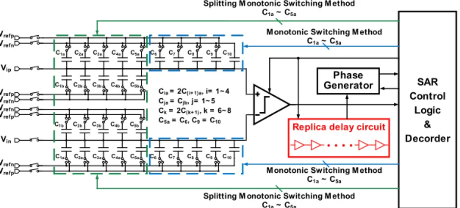
Figure 1 shows the architecture of the proposed SAR ADC. It consists of a differential S/H circuit, a differential binary-weight DAC, a comparator, a SAR logic control and replica delay circuit for adaptive window (AW) skill. To maintain the common-mode voltage Vcm of comparator’s differential input from encountering dynamic offset, the split monotonic switching skill is implemented on the most significant bit (MSB) to MSB − 4 capacitors and the capacitors are split into half of the original size. Besides, the linearity of the sample and hold circuit in a low supply voltage system should also be concerned. We apply double boost strapped switch skill which creates a constant voltage difference “2VDD” between the gate and source termination and lower down the on resistance of the switches. The replica delay circuit duplicates the operation time of the dynamic comparator. To record the operation time, both the trigger signals of dynamic comparator and replica delay circuit are Clkc. More details will be discussed in the subsection II.B.
The proposed architecture includes redundant ranges which can tolerate the DAC settling errors and comparison errors in the conversions, however we do not need extra capacitors or cycles.
B. Adaptive Window
While SAR operation performs a low energy, there are some parts to be improved. The comparator and DAC in low voltage supply are relative power consuming part of an SAR ADC. One can adopt low power switching method [7][8] or window function [1][2][3][4] to decrease power consumption.
In order to fully utilize the benefit of the voltage window function, we need another source domain information to distinguish the input range. The information may be roughly but much faster. By sensing the comparison time, we can obtain the difference of the input signal. The larger input signal is; the comparator works faster. Consider comparator as a single-pole response [3], the comparator function can be expressed as follows:
= ( )e( ) (1) where A is the gain of comparator, is the comparator input voltage, is the available comparator output for backend digital circuits and is the time constant. This operation time varies linearly as the full-scale voltage scaled down. The comparison time of each stage in full-scale can be modeled as follow:
( )− ( ) = ( ( )) (2) where ( ) is a constant term. Figure 2 shows the variation time of a dynamic comparator.
As we know from above that the voltage domain information can be transferred into time domain and it varies in grade. It helps ADC predict the input range while comparing which can be applied to window function. Figure 3 shows the circuit diagram of proposed adaptive window skill. Clkc is the active signal of dynamic comparator and also replica delay circuit. While the comparator is operating, replica delay circuit records the time concurrently. The delay circuit creates five timing scales which correspond to voltage windows of the first five stages. Each window scale is between half to quarter full-scale of the current stage. If the voltage comparator does not output the result before the replica delay circuit reaches the first window, the window function will be triggered. Once the first window is triggered, the replica delay circuit continues counting for the second window and so on. Until comparator outputs the result, the replica delay circuit stops counting. Next, digital circuit and replica delay circuit give phase generator information to decide which stage of the capacitor should be switched. If the voltage comparator outputs the result before the replica delay circuit, the SAR ADC works as a conventional one.
Figure 4 shows the timing diagram of the conventional ternary SAR ADC and proposed adaptive window SAR ADC with the same inputs. When the voltage comparator is activated, both the replica delay circuit starts to count for the first timing window. If the voltage comparator not outputs the result before the delay circuit stops, the window function will be triggered. However, the ternary SAR ADC’s comparator start to reset for the next comparison and so does the replica delay circuit. While adaptive window SAR ADC’s Fig. 1. The architecture of the proposed 10-bit SAR ADC.
C1a C2a C3a C4a C5a C6 C7 C8 C9 C10
C1b C2b C3b C4b C5b
Phase Generator
Replica delay circuit
C1a C2a C3a C4a C5a C6 C7 C8 C9 C10 C1b C2b C3b C4b C5b
SAR Control
Logic
&
Decorder
Cia = 2C(i+ 1)a, i= 1~ 4 Cja = Cjb, j= 1~ 5 Ck = 2C(k+ 1), k = 6~ 8 C5a = C6, C9 = C10
Splitting M onotonic Switching M ethod C1a ~ C5a
Monotonic Switching M ethod C1a ~ C5a
Monotonic Switching M ethod C1a ~ C5a
Splitting M onotonic Switching M ethod C1a ~ C5a
Vrefp
Vrefn
Vrefp
Vrefn
Vrefn
Vrefp
Vrefn
Vrefp
Vip
Vin
Fig. 3. Comparator operation time versus the full-scale input signal of each stage.
valid clkc clks
clk1 clk2 clk9
Bitp1Bitn1 Bitp2Bitn2 Bitp9Bitn9
Replica delay circuit
Once- triggered
latch Phase
gen.
tri
EN
tri
EN
tri
EN
Fig. 2. Comparator operation time versus the full-scale input signal of each stage.
comparator keeps operating and it takes the advantage of the delay time from former window. As the window gets smaller, the corresponding delay time grows longer. Adaptive window reuses the delay which was created for previous window which not only saves time from reset and repeatable delay, but also decreases the power of both replica delay circuit and dynamic comparator.
C. Control Circuit
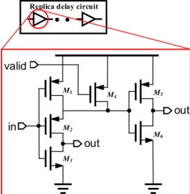
To perform the adaptive window skill, the replica delay circuit has been adopted in proposed SAR ADC. However, the implementation of the method requires additional control circuits which receive the signals from comparator and replica delay circuits. For a conventional asynchronous SAR ADC, one needs to create Clki signal to indicate which stage is processing in order to switch corresponding capacitors.
Usually we apply shift register [7] or compact [9] to create Clki. The proposed adaptive window skill only needs to add once-triggered latches to conventional compact to realize control function. Figure 3 also shows the modified compact circuit for adaptive window. Clki comes from two sources.
The first one is from differential capacitor. If either one of the capacitors of current stage is switched, the stage is regarded
as finished. However, while the window function is triggered, both the capacitors remain non-switch. At this situation, the Clki signal comes from replica delay circuit. To keep the Clki high through all conversion till sample signal reset, we apply once-triggered latch to maintain the result of the replica delay circuit.
Figure 5 shows the circuit of a unit buffer of replica delay circuit. In order to lower down the power consumption, one needs to increase the delay time with less loading. The buffer is designed with skew to get more delay in main path and fast settle in reset phase. Moreover, M2 and M3 are separated and cascaded. First, intentionally induce body effect to M2, which increase the threshold voltage with source voltage. Second, the effect of drain-induced barrier lowering (DIBL) which also increases the threshold voltage and increases delay with less power consumption.
III. SIMULATION RESULTS
The proposed SAR ADC was designed in TSMC TN90GUTM 90nm CMOS process. The test chip area is 0.8836 mm2, and core circuits occupy 0.04 mm2. The chip layout is shown in Figure 6.
The post-simulation result on TABLE I. shows the variation of first and second window between different corner.
Fig. 6. Die photo.
Fig. 5. The circuit diagram of unit buffer of replica delay circuit.
out valid
in
out
M1
M2
M3
M4 M5
M6
Replica delay circuit
Fig. 4. The timing diagram of (a) ternary SAR and (b) adaptive window SAR with same input.
Reset T V-comp
V-comp TDC
V-comp V-comp
DAC
Reset Reset Reset V-comp
TDC
DAC
V-comp TDC TDC
V-comp V-comp
TDC DAC
Voltage comparator active Replica delay circuit
DAC settle Output a bit
TDC TDC TDC TDC T TDC
(a)
(b)
The two extreme cases of first window vary from 0.391 to 0.483 Vref, and second window vary from 0.147 to 0.240 Vref respectively. To prevent DAC array from non-convergence, the window size should not be larger than half of the stage full-scale. Therefore, the redundancy range variations in both cycles do not distort the operations.
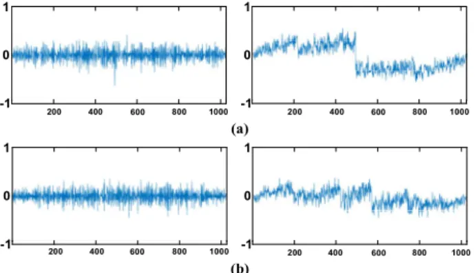
The measured differential non-linearity (DNL) and integral non-linearity (INL) is plotted in Figure 7 where peak values are -0.45/0.37 and -0.42/0.37 LSB, respectively. The measured SNDR achieves 57.18dB (ENOB is 9.21 bits) at 100KS/s with 50KHz input.
The circuit operates at 0.35 V supply voltage and the total power consumption with and without adaptive window is 74.04 nW and 85.33 nW respectively. As a consequence, the skill reduces about 13% power consumption of whole SAR ADC. The figure-of-merit (FoM) is 1.25 fJ/Conv.-step. Table II. shows the similar-resolution comparison result among this work and other state-of-the-art SAR ADCs.
IV. CONCLUSION
This paper presents a circuit technique which combines the advantages of static window and dynamic window.
Adaptive window optimizes the window size to give SAR ADC not only more redundant ranges but also decrease power consumption. Furthermore, the window function omits unnecessary switching, which diminishes the impacts of capacitor mismatch. The simulation results demonstrate the effectiveness in enhancing the performance and robustness for the SAR ADCs.
ACKNOWLEDGMENT
This work was supported by the grant from Ministry of Science and Technology in Taiwan under Grant MOST (105- 2221-E-006-240-MY3).
REFERENCES
[1] G. Y. Huang, S. J. Chang, C. C. Liu and Y. Z. Lin, “A 1-µW 10-bit 200-kS/s SAR ADC With a Bypass Window for Biomedical Applications,” in IEEE Journal of Solid-State Circuits, vol. 47, no. 11, pp. 2783–2795, Nov. 2012.
[2] C. C. Liu, S. J. Chang, G. Y. Huang, Y. Z. Lin and C. M. Huang, “A 1V 11fJ/conversion-step 10bit 10MS/s asynchronous SAR ADC in 0.18µm CMOS,” in IEEE Symp. VLSI Circuits Dig. Tech. Papers, 2010, pp.241–242.
[3] J. Guerber, H. Venkatram, M. Gande, A. Waters and U. K. Moon, “A 10-b Ternary SAR ADC With Quantization Time Information Utilization,” in IEEE Journal of Solid-State Circuits, vol. 47, no. 11, pp. 2604–2613, Nov. 2012..
[4] Y. H. Chung, M. H. Wu and H. S. Li, “A 24μW 12b 1MS/s 68.3dB SNDR SAR ADC with two-step decision DAC switching,” in IEEE Custom Integrated Circuits Conference, 2013, pp. 1–4.
[5] Y. H. Chung, C. H. Tsai and H. C. Yeh, “A 5-b 1-GS/s 2.7-mW binary- search ADC in 90nm digital CMOS,” in IEEE International System- on-Chip Conference, 2015, pp. 25–29.
[6] Y.-H. Chung, “The Swapping Binary-Window DAC Switching Technique for SAR ADCs,” in Proc. IEEE ISCAS, 2013, pp. 2231–
2234.
[7] Chun-Cheng Liu, Soon-Jyh Chang, Guan-Ying Huang, and Ying-Zu Lin, “A 10-bit 50-MS/s SAR ADC with a Monotonic Capacitor Switching Procedure,” in IEEE Journal of Solid-State Circuits, vol.45, no.4, pp.731–740, Apr. 2010.
[8] V. Hariprasath, J. Guerber, S. H. Lee and U. K. Moon, “Merged capacitor switching based SAR ADC with highest switching energy- efficiency,” in IEEE Electronics Letters, vol. 46, no. 9, pp. 620–621, April 29 2010.
[9] Che-Hsun Kuo and Soon-Jyh Chang “A 10–bit 120–MS/s SAR ADC with compact architecture and noise suppression technique, ” Department of Electrical Engineering, National Cheng Kung University, Tainan, Taiwan,Thesis for Master of Science, July, 2014 [10] P. Harpe, H. Gao, R. van Dommele, E. Cantatore and A. van
Roermund, “21.2 A 3nW signal-acquisition IC integrating an amplifier with 2.1 NEF and a 1.5fJ/conv-step ADC,” in IEEE International Solid-State Circuits Conference Dig. Tech. Papers, 2015, pp. 1–3.
[11] S. Jeong et al., "A 120nW 8b sub-ranging SAR ADC with signal- dependent charge recycling for biomedical applications,” in IEEE Symp. VLSI Circuits Dig. Tech. Papers, 2015, pp. C60–C61.
[12] H. Y. Tai, H. W. Chen and H. S. Chen, “A 3.2fJ/c.-s. 0.35V 10b 100KS/s SAR ADC in 90nm CMOS,” in IEEE Symp. VLSI Circuits Dig. Tech. Papers, 2012, pp. 92-93.
TABLE I. CORNER VARIATION OF REPLICA DELAY CIRCUIT Voltage
variation TT FF FS SF SS
Window #1 0.450 Vref
0.444 Vref
0.391 Vref
0.457 Vref
0.483 Vref
Window #2 0.219 Vref
0.147 Vref
0.205 Vref
0.126 Vref
0.240 Vref
Fig. 7. The measured DNL and INL (a) without and (b) with adaptive window.
(a)
(b) 1
-1 0
200 400 600 800 1000
1
-1 0
200 400 600 800 1000
1
-1 0
200 400 600 800 1000
1
-1 0
200 400 600 800 1000
TABLE II. PERFORMANCE SUMMARY AND COMPARISON WITH THE STATE-
OF-THE-ART ADCS. ISSCC’15
[10] VLSI’15
[11] VLSI’12
[6] This Work
Technology(nm) 65 180 90 90
Supply Voltage(V) 0.6 0.6 0.35 0.35
Sampling
Rate(KS/s) 100 100 100 100
Resolution(bit) 10 8 10 10
Nyquist SNDR(dB) 57.3 46.9 56.3 57.18
Power(nW) 88 120 170 74
FoM(fJ/step) 1.5 6.6 3.2 1.25
105年度專題研究計畫成果彙整表
計畫主持人:張順志 計畫編號:105-2221-E-006-240-MY3 計畫名稱:具高安全性且易於整合的車用類比至數位轉換器之研製
成果項目 量化 單位
質化
(說明:各成果項目請附佐證資料或細 項說明,如期刊名稱、年份、卷期、起 訖頁數、證號...等)
國 內
學術性論文
期刊論文 0
研討會論文 1 篇 SEMBA為生醫電子領域重要會議。
專書 0 本
專書論文 0 章
技術報告 0 篇
其他 0 篇
智慧財產權 及成果
專利權 發明專利 申請中 0
件
已獲得 0
新型/設計專利 0
商標權 0
營業秘密 0
積體電路電路布局權 0
著作權 0
品種權 0
其他 0
技術移轉 件數 0 件
收入 0 千元
國 外
學術性論文
期刊論文 1
篇
IEEE Transactions on Circuits and Systems I: Regular Papers為Circuits and Systems最具代表性的期刊。
研討會論文 4
ISCAS為Circuits & Systems領域旗艦會 議。
VLSI-DAT為台灣舉辦的重點國際學術會 議。
專書 0 本
專書論文 0 章
技術報告 0 篇
其他 0 篇
智慧財產權 及成果
專利權 發明專利 申請中 0 件
已獲得 0
新型/設計專利 0
商標權 0
營業秘密 0