A Smart Control Approach for Digitally Controlled Multiple-Output DC-DC Converter
Fujio Kurokawa
Nagasaki University Nagasaki, 852-8521 Japan [email protected]
Tomoyuki Mizoguchi
Nagasaki University Nagasaki, 852-8521 Japan [email protected]
Yuichiro Shibata
Nagasaki University Nagasaki, 852-8521 Japan [email protected]
Masato Soejima
Nagasaki University Nagasaki, 852-8521 Japan [email protected]
Hiroyuki Osuga
Mitsubishi Electronic Corporation Kamakura, 247-8520 Japan
[email protected] Abstract --This paper presents a smart control approach for
digitally controlled forward type multiple-output dc-dc converter. In this case, the central problem of design is how to decide the integral coefficient. Since the decision of integral coefficient depends on the static characteristics, the selected integral coefficient is not suitable to perform the superior dynamic characteristics. Then, it is important to set the suitable the integral coefficient for not only static characteristics but also dynamic characteristics. As a result, overshoot and the convergence time of the output voltage are improved 30% and 30%. The overshoot of reactor current is improved 11%.
Moreover, to achieve the improvement of the dynamic characteristic, the number of bits of the calculation part of the digital control circuit set enlarged. As a result, the overshoot and the convergence time of the output voltage are improved 78% and 30%. The overshoot of reactor current is improved 17%.
Index Terms-- Digital control, Forward type multiple-output dc-dc converter
I. INTRODUCTION
The saving energy in the power supply has been brought to public attention. A popular idea exists nowadays that the energy management is useful to reduce the total electric power consumption in switching power supply system.
However, this technology is not widely used because the conventional analog controller is not able to connect the control network of the energy management power supply system easily. Therefore, since the digital control circuit is fundamentally consist of the digital signal one, the concern with the digital control for switching power supply has been growing to construct the digital interconnection energy management power supply system. Recently, a considerable number of studies have been made on a digital control [1], [2]. At a first step, it may be helpful to begin with a study of the approach for design of the digital control. The central problem of design for digital control circuit is how to decide the integral coefficient. Since the decision of integral coefficient depends on the static characteristics, the integral coefficient is not suitable to perform the superior dynamic characteristics. In this paper, the main circuit consists of the
forward type multiple-output dc-dc converter [3], [4]. This circuit is a good example to examine a design of the digital control circuit for the dc-dc converter because that is widely used in the electrical and electronic systems.
This paper presents a smart control approach for digitally controlled multiple-output DC-DC converter. In this case, it is important to set the suitable integral coefficient for not only static characteristics but also dynamic characteristics. At first, we calculate the regulation range of input voltage and output current. It set the upper and lower ranges of input voltage and output current of regulation range. Next, we search the integral coefficient to satisfy the specific regulation range and then confirm the dynamic characteristic by the simulation. As a result, the overshoot and the convergence time of the output voltage are improved 30% and 30%. The overshoot of reactor current is improved 11%. Moreover, to achieve the improvement of the dynamic characteristic, the number of bits of the calculation part of the digital control circuit set enlarged. Therefore, the overshoot and the convergence time of the output voltage are improved 78% and 30% lastly.
The overshoot of reactor current is improved 17%.
II. OPERATION PRINCIPLE
Figure 1 shows the forward type multi-output dc-dc converter. In the circuit, the reset winding Np2 is added to avoid the saturated flux. The turn ratio Np1/ Np2 is equal to unity. Ei is the input voltage, eo1 and eo2 are the output voltages, respectively. io1 and io2 are the output currents. iL1 and iL2 are the reactor currents. D11, D12, D21 and D22 are the diodes. C1 and C2 are the output smoothing capacitors. Np1, Np2, Ns1 and Ns2 are the numbers of turn for the transformer T. R1 and R2 are the loads. L is energy storage reactor with the cross regulation function. NL1 and NL2 are the number of turn for energy storage reactor L.
The output voltage eo1 is detected and is controlled.
Another output voltage eo2 is controlled by the cross regulation of the transformer T and reactor L. The following equation is related the turn ratio and output voltage.
PEDS2009
1* Eo
2* Eo 1 NL
2 NL
= (1) Figure 2 shows the digital control circuit of forward type multi-output dc-dc converter. The output voltage eo1 is the control target. eo1 is sent to the A-D converter through the anti-aliasing filter and is converted into digital amount Nn.
The relation between the input and output values of the A- D converter is given by Eq. (2) when it approximately shows the linear expression by considering the width of the quantization to be small.
n , 1 eo AGAD
Nn = (2) where n denotes a n-th switching cycle and the digital amount Nn is a positive integer number. A is the gain of the anti- aliasing filter. GAD is the gain of the A-D converter.
max AD , 1 eo
max , Nn
GAD = (3) The digital amount Nn is sent to the calculation part. The PID control is performed by the calculated part as shown the following equation,
(
Nn NR)
KP NB 1 n ,
NTon + = − −
−KI∑
(
Nn−NINT)
−KD(
Nn−Nn−1)
(4)where KP, KI and KD are the proportional, integral and differential coefficients, NR and NINT are the reference value of the proportional and integral parts, respectively. NB is the basic value, rTr is on-resistance of Tr, rT is resistance of the transformer and rL1 is resistance of the inductance.
Eo1* are the reference value of the output voltage NB is represented as follows;
( )
2) Io R1
*o1 E p( i r 1E Np 1 Ns
1 Eo R1
1 rL Ts1 B N
N − +
+ ∗
= (5)
where
rT rTr
rp = + (6) The numerical value equivalent to the width is turned on with NTon and it's set in a PWM signal generation circuit.
When the number of bits of the A-D converter is set to QAD, NTs is given by the following equation.
AD 1 2Q
NTs≤ − (7) The duty ratio STon/Ts is represented as follows;
NTs Ts N /
STon = Ton,n+1
(8)
Next, the regulation characteristic of the output voltage is discussed using an ideal transformer. The on-time Toni in the steady-state is shown as follows;
( ) )
2 Io 1 Io p( i r 1E Np 1 Ns
1 Eo R1
1 rL s1 oni T
T − +
+ ∗
= (9)
However, the leakage inductance Ll changes the on-time into the commutation time Tc1 and Tc2 in an actual transformer because it influences and the commutation time becomes long.
Tc1 and Tc2 are shown as follows.
Ei 1 Io Ll 1 Ns
1 Np 2 Tc 1
Tc = = (10) Therefore, to control the forward type multiple-output dc-dc converter, the on-time in which it tempers with Toni, the rectification time Tc1, and Tc2 are needed. The range of the on/off ratio of switch Tr where the overflow and the underflow with the integration control circuit are not caused is shown based on this expression (9) and expression (10) as follows.
However, the maximum value of the integer with the sign of the QI bits becomes 2QI-1-1 in the operation part and the minimum value of the negative value becomes -2QI-1 because it uses the highest-order digit for the sign bit.
Fig.2 Digital control circuit.
e S
Calculation Part
PWM Signal Generator OSC
CLK
A-D Converter
Anti-Aliasing Filter Nn
NTon
Ton/Ts eo1
S
Calculation Part
PWM Signal Generator OSC
CLK
A-D Converter
Anti-Aliasing Filter Nn
NTon
Ton/Ts o1
DR
T
E N e
N N D C R
R
D C
N
e i i Digital Control
Circuit Drive
Circuit
N N
L
D D T
i i
i r
p1
p2
s1 11
12
21
22 L1
L2 L1
L2 1
2 o2 o1
o1
o2 1
s2 2 DR
T
E N e
N N D C R
R
D C
N
e i i Digital Control
Circuit Drive
Circuit
N N
L
D D T
i i
i r
p1
p2
s1 11
12
21
22 L1
L2 L1
L2 1
2 o2 o1
o1
o2 1
s2 2
Fig.1 Digitally controlled multiple-output DC-DC converter.
PEDS2009
NTs 1 2QI KI NB Ts EiIlo1 L 1 Ns
1 Np 2) Io 1 Io p( i r 1E Np 1
Ns (1 rL1R1)Eo1 NTs
) 1 1 2QI I ( B K
N + < + × −
+
− + ∗
− <
× −
−
(11) The regulation range against input voltage is represented as follows;
1 ae 2
1c ae 2 4 1 be 1 be Ei 1
ae 2
2c ae 2 4 2 be 2
be + −
<
− <
+ (12)
where
Z1 1 Np
s1 1 N
ae = (13)
Z2 1 Np
s1 N 2
ae = (14)
Z1 2) Io 1 Io p(
* r 1 Eo 1) 1 R rL 1 s ( T
1 Io Ll 1
be = + + + + (15)
Z2 2) Io 1 Io p(
* r 1 Eo 1) 1 R rL 1 s ( T
1 Io Ll 2
be = + + + + (16)
2) Io 1 Io p( r Ts
1 Io Ll
c=− + (17)
NTs ) 1 1 QI 2 I ( B K 1 N
Z = − × − − (18)
NTs I 1 2Q KI NB
Z2= + × − (19) The regulation range against output current is represented as follows;
ai 2
2 ci 2 ai 2 4 2 bi 2 bi 1 Io ai
2
1 ci 1 ai 2 4 1 bi 1
bi + − < < + − (20)
where
rp Ts Ei
Ll 1 Np
s1
a=− N (21)
rp Z1 1) Io rp Ei 1 Np
s1 (N Ts Ei
Ll 1 Np
s1 N 1
bi =− − − (22)
rp Z2 1) Io rp Ei 1 Np
s1 (N Ts Ei
Ll 1 Np
s1 2 N
bi =− − − (23)
+ ∗
−
−
= Ei rpIo1) (1 rL1 R1)Eo1 N
s1 (N Z1 1
ci (24)
+ ∗
−
−
= Ei rpIo1) (1 rL1 R1)Eo1 1
Np s1 (N Z2 2
ci (25)
III. THESMARTAPPROACHFORDESIGNAND RESULTOFSIMULATIONANDEXPERIMENT The circuit parameters are C1=C2=960μF, Np1:Np2:
Ns1:Ns2=2:2:1:2, Eo1*=5V, Eo2*=10V and R2=20Ω. The inductance L is 98μH. Furthermore, QAD = 12bits, GAD = 819V-1 and NTS = 4000. The sampling frequency fsmp is equal to the switching frequency fs and is 100kHz.
The digital PWM module is made from an Xilinx Vertex-
Ⅱpro FPGA. Figure 3 shows the construction of digital PWM. It makes clock that moves four phases of 100MHz in the DCM (Digital Clock Manager). As a result, the counter with the performance of 400MHz becomes suitable [5], [6].
A. Static Characteristics
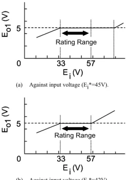
The regulation range against the output voltage and current is shown in Eqs. (12) and (20). As shown in these equations, the regulation range depends on KI and QI. In this case, the rating input voltage Ei* is 45V and the specification of the regulation range of the output voltage is set from 33V to 57V. However, when the rating input voltage is 45V, the upper input voltage range is more over the specific regulation range as shown in Fig. 4(a). So, we search the new suitable rating input voltage 42V as shown in Fig. 4(b). Figure 5 shows the relationship between the number QI of bits of the calculation part and the digital integral coefficient KImin. In this figure, the dot line denotes the condition of Ei*=45V and the solid line shows the relationship in Ei*=42V. It is seen that KImin in case of Ei*=42V is smaller than that in case of Ei*=45V against each QI and the integral coefficient KI can be selected small when the number of bits is large.
Furthermore, the good regulation from no load to full load is obtained as shown in Fig. 6 because the mmf (magneto motive force) of the reactor L is continuous in Fig. 1 and regulation range is enough wide [7], [8].
Fig. 3 Construction of digital PWM.
DCM
PWM CLK
3π/2 Delay π
Delay Delay π/2
DCM
PWM PWM CLK
3π/2 Delay π
Delay Delay π/2
PEDS2009
B. Dynamic Characteristics
Figures 7, 8 and 9 show the simulated transient response when the load R1 is step changed from 50Ω to 5Ω. In Fig. 7, the circuit parameters are same to Fig. 4(a). In Fig. 8 and 9, the circuit parameters are same to Fig. 4(b). The simulator is PSIM.
In Figs. 7, 8 and 9, KP is equal to 2, KD is equal to 2 and KI is changed as parameters. Figure 7 shows that the overshoot and undershoot of the output voltage eo1 are over 2.8 % and 4.5% in case of KI = 0.03 and QI=15bits. The convergence time tst that the output voltage eo1 is settled within 1% is equal to 4.0ms. The overshoot of reactor current is over 97%. Figure 8 shows that the overshoot and undershoot of the output voltage eo1 are over 2.1% and 4.6%
in case of KI = 0.022 and QI=15bits. The convergence time tst that the output voltage eo1 is settled within 1% is 3.1ms.
The overshoot of reactor current is over 90%. Next, to achieve the improvement of the dynamic characteristic, the number of bits of the calculation part of the digital control circuit QI set enlarged. Figure 9 shows that the overshoot and undershoot of the output voltage eo1 is over 0.7% and 4.7%
in case of KI = 0.011 and QI=16bits. The convergence time tst that the output voltage eo1 is settled within 1% is 3.0ms.
The overshoot of reactor current is over 77%.
It is seen that the overshoot, the convergence time tst of the output voltage eo1 and the overshoot of reactor current iL1 are improved in case of the new suitable rating input voltage. Moreover, transient responses are improved when the number of bits of the calculation part of the digital control circuit QI set enlarged.
Figures 10, 11 and 12 show the experimental transient response are step change the same as simulation.
Figure 10 shows that the overshoot and undershoot of the output voltage eo1 is over 2.7%, 4.3% in case of KI =0.03 and QI=15bits. The convergence time tst that the output voltage eo1 is settled within 1% is 4.0ms. The overshoot of reactor current is over 97%. Figure 11 shows that the overshoot and undershoot of the output voltage eo1 are over 1.9%, 4.1% in case of KI = 0.022 and QI=15bits. The convergence time tst that the output voltage eo1 is settled within 1% is 3.2ms. The overshoot of reactor current is over 86%. Next, to achieve the improvement of the dynamic characteristic, the number of bits of the calculation part of the digital control circuit QI set enlarged. Figure 12 shows that the overshoot and undershoot of the output voltage eo1 are over 0.6% and 4.3% in case of KI = 0.011 and QI = 16bits.
The convergence time tst that the output voltage eo1 is settled within 1% is 3.2ms. The overshoot of reactor current is over 81%.
It is seen that the transient response is improved as same as the simulated results.
0 5 10
0 0.5 1 1.5 2
E (V)o1
I (A)o1
0 0.5 1.0 1.5 2.0 5
10
0 5 10
0 0.5 1 1.5 2
E (V)o1E (V)o1
I (A)o1
0 0.5 1.0 1.5 2.0 5
10
Fig. 6 Regulation characteristics against output current Io1 (Experimental result).
Fig.5 Relationship between QI and KImin against regulation range (Calculated result).
0.02
K
14 15 16
QI (bits) 0.00
0.04
Imin
0.06 △: E *=45V
○: E *=42Vi i
0.02
K
14 15 16
QI (bits) 0.00
0.04
Imin
0.06 △: E *=45V
○: E *=42Vi i
Fig. 4 Regulation characteristics against input voltage Ei.
(a) Against input voltage (Ei*=45V).
(b) Against input voltage (Ei*=42V).
E (V)
E (V) 33 5
57 0
i
o1
Rating Range
E (V)
E (V) 33 5
57 0
i
o1
Rating Range
E (V)
E (V) 33 5
57 0
i Rating Range
o1E (V)
E (V) 33 5
57 0
i Rating Range
o1
PEDS2009
(a) Output voltage eo1.
Vertical : 100mV/div, Horizontal : 2ms/div.
(b) Reactor current iL1.
Vertical : 500mA/div, Horizontal : 2ms/div.
Fig. 10 Transient response in case of KI=0.03 and QI=15bits Overshoot : 2.7%
Unsershoot : 4.3%
t : 4.0msst Overshoot : 2.7%
Unsershoot : 4.3%
t : 4.0msst t : 4.0msst
Overshoot : 97%
Overshoot : 97%
(a) Output voltage eo1.
(b) Reactor current iL1.
Fig. 9 Transient response in case of KI=0.011 and QI=16bits (Simulated results).
5.3
5.0 4.9
4.7
e(V)
4.0 0.0 1.0 2.0 3.0
t (ms) 4.8
5.1 5.2
o1
Overshoot : 0.7%
Undershoot :4.7%
±1%
t :3.0msst 5.3
5.0 4.9
4.7
e(V)
4.0 0.0 1.0 2.0 3.0
t (ms) 4.8
5.1 5.2
o1
5.3
5.0 4.9
4.7
e(V)
4.0 0.0 1.0 2.0 3.0
t (ms) 4.8
5.1 5.2
o1
5.3
5.0 4.9
4.7
e(V)
4.0 0.0 1.0 2.0 3.0
t (ms) 4.8
5.1 5.2
o1
Overshoot : 0.7%
Undershoot :4.7%
±1%
t :3.0msst t :3.0msst
2.0
1.0
0.0
i (A)
4.0 0.0 1.0 2.0 3.0
t (ms)
L1
2.5
1.5
0.5
Overshoot : 77%
2.0
1.0
0.0
i (A)
4.0 0.0 1.0 2.0 3.0
t (ms)
L1
2.5
1.5
0.5 2.0
1.0
0.0
i (A)
4.0 0.0 1.0 2.0 3.0
t (ms)
L1
2.5
1.5
0.5
Overshoot : 77%
(a) Output voltage eo1.
(b) Reactor current iL1.
Fig. 8 Transient response in case of KI=0.022 and QI=15bits
5.3
5.0 4.9
4.7
e(V)
4.0 0.0 1.0 2.0 3.0
t (ms) 4.8
5.1 5.2
o1
Overshoot : 2.1%
Undershoot :4.6%
±1%
t : 3.1msst 5.3
5.0 4.9
4.7
e(V)
4.0 0.0 1.0 2.0 3.0
t (ms) 4.8
5.1 5.2
o1
5.3
5.0 4.9
4.7
e(V)
4.0 0.0 1.0 2.0 3.0
t (ms) 4.8
5.1 5.2
o1
5.3
5.0 4.9
4.7
e(V)
4.0 0.0 1.0 2.0 3.0
t (ms) 4.8
5.1 5.2
o1
Overshoot : 2.1%
Undershoot :4.6%
±1%
t : 3.1msst t : 3.1msst
Overshoot : 90%
2.0
1.0
0.0
i (A)
4.0 0.0 1.0 2.0 3.0
t (ms)
L1
2.5
1.5
0.5
Overshoot : 90%
2.0
1.0
0.0
i (A)
4.0 0.0 1.0 2.0 3.0
t (ms)
L1
2.5
1.5
0.5 2.0
1.0
0.0
i (A)
4.0 0.0 1.0 2.0 3.0
t (ms)
L1
2.5
1.5
0.5
(a) Output voltage eo1.
(b) Reactor current iL1.
Fig. 7 Transient response in case of KI=0.03 and QI=15bits (Simulated results).
5.3
5.0 4.9
4.7
e(V)
4.0 0.0 1.0 2.0 3.0
t (ms) 4.8
5.1 5.2
o1
Overshoot : 2.8%
Undershoot :4.5%
±1%
t : 4.0msst 5.3
5.0 4.9
4.7
e(V)
4.0 0.0 1.0 2.0 3.0
t (ms) 4.8
5.1 5.2
o1
5.3
5.0 4.9
4.7
e(V)
4.0 0.0 1.0 2.0 3.0
t (ms) 4.8
5.1 5.2
o1
Overshoot : 2.8%
Undershoot :4.5%
±1%
t : 4.0msst t : 4.0msst
2.0
1.0
0.0
i (A)
4.0 0.0 1.0 2.0 3.0
t (ms)
L1
2.5
1.5
0.5
Overshoot : 97%
2.0
1.0
0.0
i (A)
4.0 0.0 1.0 2.0 3.0
t (ms)
L1
2.5
1.5
0.5 2.0
1.0
0.0
i (A)
4.0 0.0 1.0 2.0 3.0
t (ms)
L1
2.5
1.5
0.5
Overshoot : 97%
PEDS2009
IV. CONCLUSION
The transient response to step change of the load is discussed in the digital control circuit for the forward type multi-output DC-DC converter. Moreover, it introduced the smart approach for design of digital control.
It is important to set the suitable integral coefficient for not only static characteristics but also dynamic characteristics.
It seems that excellent characteristic is obtained when the new suitable rating input voltage is selected. As a result, overshoot and the convergence time of the output voltage are improved 30% and 30%. The overshoot of reactor current is improved 11%.
Moreover, to achieve the improvement of the dynamic characteristic, the number of bits of the calculation part of the digital control circuit set enlarged. Lastly, it is revealed that the overshoot and the convergence time of the output voltage are improved 78% and 30%. Furthermore, the overshoot of reactor current is improved 17%.
ACKNOWLEDGMENT
This work is supported in part by the Grant-in-Aid for Scientific Research (No.21360134) of JSPS (Japan Society for the Promotion of Science) and the Ministry of Education, Science, Sports and Culture.
REFERENCES
[1] P. T. Krein, “Digital control generations -digital controls for power electronics through the third generation,” IEEE PEDS. Nov. 2007.
[2] F. Kurokawa, W. Okamoto and H. Matsuo, “A comparison of steady-state characteristics of buck-type dc-dc converter using DSP,” Invited Paper, Wiley Periodicals, Inc., Electronics and Communications in Japan, vol. 90, no. 5, pp. 1-10, May 2007.
[3] H. Matsuo and F. Kurokawa, “Analysis of multiple-output dc-dc power converter using cross-regulation,” Trans. IECE, vol.62-C, no.8, August 1979.
[4] H. Saotome, S. Oikawa, Y. Kikuchi, N. Sekino and M. Hayashi,
“Analysis of cross-regulation in multiple-output dc/dc converters,”
Trans. IEICE of Japan, vol. 104, no.407, pp. 25-30, Nov. 2004.
[5] M. Milanovic, M. Truntic and P. Slibar, “FPGA implementation of digital controller for dc-dc buck converter,” Proc. IWSOC, pp.439- 443, 2005.
[6] H.-J.Guo, Y. Shiroishi and O. Ichinokura, “Digital PI controller for high frequency switching dc/dc converters based on FPGA,” Proc.
INTELEC, pp.536-541, 2003.
[7] H. Matsuo and F. Kurokawa, “Analysis of multiple-output dc-dc power converter using cross-regulation,” Trans. IECE, vol. 62-C, no.8, August 1979.
[8] K Park, H. Seong, H. Kim, G. Moon and M. Youn, “Multi-Level active clamp forward converter with reduced voltage stress,” IEEE Power Electronics Specialists Conference Record, pp.938-943, June 2008.
(a) Output voltage eo1.
Vertical : 500mV/div., Horizontal : 21ms/div.
(b) Reactor current iL1.
Vertical : 500mA/div, Horizontal : 21ms/div.
Fig. 11 Transient response in case of KI=0.011 and QI=16bits (Experimental results).
Overshoot : 0.6%
Unsershoot : 4.3%
t : 3.2msst Overshoot : 0.6%
Unsershoot : 4.3%
t : 3.2msst t : 3.2msst
Overshoot : 81%
Overshoot : 81%
(a) Output voltage eo1.
Vertical : 100mV/div, Horizontal : 2ms/div.
(b) Reactor current iL1.
Vertical : 500mA/div, Horizontal : 2ms/div.
Fig. 11 Transient response in case of KI=0.022 and QI=15bits (Experimental results).
Overshoot : 86%
Overshoot : 86%
Overshoot : 1.9%
Unsershoot : 4.1%
t : 3.2msst Overshoot : 1.9%
Unsershoot : 4.1%
t : 3.2msst t : 3.2msst
PEDS2009