1
國立成功大學新進教師學術研究計畫成
果報告
應用於高可靠度奈米元件之內連線材料
其成長與特性之研究
計畫執行單位:國立成功大學材料科學及工程學系
計畫主持人:呂國彰
助理教授
中 華 民 國 102 年 4 月
2
報告摘要:
We report the critical effects of oxide on the growth of nanostructures through silicide formation. Under an in situ ultrahigh vacuum transmission electron microscope, it is observed from the conversion of Si nanowires into the metallic PtSi grains epitaxially through controlled reactions between lithographically defined Pt pads and Si nanowires. With oxide, instead of contact area, single crystal PtSi grains start forming either near the center between two adjacent pads or from the ends of Si nanowires, resulting in the heterostructure formation of Si/PtSi/Si. Without oxide, transformation from Si into PtSi begins at the contact area between them, resulting in the heterostructure formation of PtSi/Si/PtSi. The nanowire heterostructures have an atomically sharp interface with epitaxial relationships of Si(20-2)//PtSi(10-1) and Si[111]//PtSi[111]. Additionally, it has been observed that the existence of oxide significantly affects not only the growth position but also the growth behavior and growth rate by two orders of magnitude. Molecular dynamics simulations have been performed to support our experimental results and the proposed growth mechanisms. In addition to fundamental science, the significance of the study matters for future processing techniques in nanotechnology and related applications as well.
本研究透過矽化物之生成探討氧化層對於成長奈米結構之影響。首先利用微 影技術定位出鉑墊並與矽奈米線接合並利用臨場穿透式電子顯微鏡觀察,發現藉 由控制鉑墊與矽奈米線的反應可使矽奈米線轉變為磊晶鉑金屬矽化物(PtSi)。當 矽奈米線具有氧化層包覆時,發現單晶 PtSi 晶粒在兩鉑墊之間的中心開始生成 進而生成 Si/PtSi/Si 異質結構。相較之下,當矽奈米線不具有氧化層時,將會 在矽與鉑墊接觸點上往矽奈米線方向開始生成 PtSi,最後得到 PtSi/Si/PtSi 異 質結構。如從原子級影像觀察會發現異質結構中 Si 與 PtSi 接面處之原子堆疊情 形為 Si(20-2)//PtSi(10-1)與 Si[111]//PtSi[111]。本研究亦發現氧化層的存 在不僅導致 PtSi 開始成長的位置不同之外,也影響其成長行為與成長速度,其 成長速度為不具氧化層的兩個數量級大。分子動力學模擬之結果更進一步地支持 此實驗之結果與成長機制。除了基礎科學上的研究貢獻外,本研究對於未來奈米 科技新製程技術之研究與應用上均有相當的重要性。
3
報告內容:
Introduction
Semiconductor nanowires (NWs) are attractive components for future nanoelectronics since they can exhibit a range of device functions and may serve as active elements in larger scale integration.1-5 Particularly, nanoscale transistors based on silicon nanowires have been extensively studied6,7 for their potentials of replacing conventional planar metal-oxide-semiconductor field-effect transistors (MOSFET) in integrated circuits3,8 and of opening new opportunities in flexible macroelectronics9-11 and highly sensitive biosensors.12,13 Oxide is a very common and important material, being indispensible especially in the semiconductor field and Si-based related processing. Additionally, here, for Si nanowires, one of the nanostructures having the greatest potential in the future, oxide was even found to be able to affect subsequent processing significantly. Metal silicides are essential as electrical contacts in our current processing of integrated circuits.14-20 Lithographically defined metal contacts are most often used in silicon nanowire transistors to facilitate the device performance. However, the formation of metal silicide nanowires and the structure and properties of silicide/silicon heterostructures have emerged as interesting problems.18,19
According to our experiences on nano-heterostructures,18,19,21 we believe the surface oxide surrounding Si nanowires is worth studying carefully for being an important factor in silicide formation at nano-scale. Platinum is an interesting interconnecting material for nano-electronics, being chemically stable in ambient or oxidizing environment. Additionally, metallic platinum silicide (PtSi) can be used as ohmic contact to p-channel Si nanowire transistors.22 Shown in our previous studies21, based on PtSi/Si/PtSi nanowire heterostructures, p-channel enhancement mode nanowire FETs with the best performance from intrinsic Si nanowires have been fabricated. Therefore, we have designed the following experiments, using controlled reactions between lithographically defined Pt pads and Si nanowires with or without oxide under in-situ transmission electron microscopy (TEM) for further investigation of the oxide effect on formation of single crystal PtSi and PtSi/Si nanowire heterostructures.
Experimental Procedures
Silicon nanowires were prepared on a p-type Si wafer by the vapor-liquid-solid (VLS) method using nano Au dots as nucleation sites. The resultant single-crystal Si nanowires are along a [111] growth direction23-25 and with thin surface oxide (~1-5 nm thick). The Si nanowires with lengths of a few microns ranged in diameter from 10 to 40 nm.
4
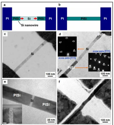
substrate using e-beam lithography and e-beam evaporation (Figure 1a and 1b). Since each of our samples contains multiple Si nanowires and there are many Pt pads deposited on a single nanowire as shown in Fig.1a and 1b, we can observe numerous examples in one sample and have done so in different samples. All of our observation supports the mechanism we report here. Prior to Pt deposition, some of the Si nanowire samples were etched in buffered hydrofluoric acid for 5 s to remove native oxide at the contact region while some were not. The etched samples were HF-dipped again prior to being loaded in UHVTEM to prevent native oxide at regions other than contact areas. Figure 1c and 1d are high resolution TEM images showing the samples with and without oxide, respectively; thereby, we can investigate the effect of native oxide on kinetics of phase transformation. For nanowires with HF dipping, no oxide was seen and the Si/oxide interface was rough; for nanowires without HF dipping, the surface oxide is of 1-2nm and the Si/oxide interface was smooth. TEM examinations were conducted in a JEOL 2000V Ultrahigh Vacuum TEM (UHV-TEM) under a base pressure of 3 x 10⁻¹⁰ Torr, where sample can be heated to 1000°C. Upon heating in UHV-TEM, Pt reacts with Si nanowires to form PtSi nanowires. Phase identification was carried out by electron diffraction pattern and energy dispersion X-ray spectrometer (EDS) analysis.
Electron beam lithography and e-beam evaporation were then used to define and deposit the Pt pads on Si nanowires (Fig. 2a). We recall that prior to Pt deposition, some of the samples were etched in buffered hydrofluoric acid for five seconds to remove native oxide. After Pt deposition, the samples are loaded into TEM and annealed in situ at 500℃ to form PtSi (Fig. 2b).
Results and Discussion
Figure 2c shows an etched Si nanowire with Pt pads on both sides before reaction. After annealing at 500℃for about 5-10 minutes, higher contrast sections with sharp interface with the Si start to emerge from both ends of the nanowire near the Pt pads, suggesting the formation of PtSi (Fig. 2d). This is attributed to the fact that many Pt atoms are able to dissolute into silicon through the long contact between the Si nanowire and the Pt pad so that supersaturation can be reached; thereby, nucleation and growth of PtSi occurs below the contact. Utilizing this phenomenon, nanowire heterostructure of PtSi/Si/PtSi in which the length of the middle Si can be precisely controlled down to sub-10 nanmometer regime (Fig. 2e). Upon further annealing, all the Si is consumed and transformed into a PtSi nanowire (Fig. 2f). Detachment of wires from pads is due to strain resulting from volume expansion.21 However, it occurs at a late stage of silicidation, while our point is at the beginning of silicidation; thus, it does not affect the behavior we observed and report. Also, if it
5
had been the stress or contact condition that matters, we should have observed incoherent behaviors among the many examples of a sample. Additionally, we have previously found that the stress effect is on the phase instead of nucleation sites.26
Based on the electron diffraction pattern corresponding to the platinum silicide region (right part of Fig. 2d), the silicide material is identified to be single crystal PtSi with an orthorhombic crystal structure having lattice constants a = 0.5567 nm, b = 0.3587 nm and c = 0.5927 nm. In addition, the epitaxial relationships between Si and PtSi has been determined as Si(20-2)//PtSi(10-1) and Si[111]//PtSi[111], according to the diffraction patterns in Fig. 2d.
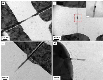
The effect of surface oxide on PtSi formation is shown in Figure 3. In the TEM images of Figure 3a and 3c, Si nanowires were HF-dipped so that they were free of oxide. At 500 ℃, PtSi forms within the Si nanowire from the contact area between the Pt pad and the Si nanowire. However, in Figure 3b and 3d, where Si nanowires were not etched with HF and they had surface oxide of 1-5 nm in thickness, PtSi forms within the Si nanowire near the center of the Si nanowire (Fig. 3b) and from the end of the Si nanowire (Fig. 3d), respectively. Since all of the phase transformations occurred in the Si nanowires, platinum atoms were the dominating diffusion species. We note that in Figure 3a and 3b, the Si nanowire was across two Pt contact pads, yet in Figure 3c and 3d, the Si nanowire was an over-hang from one Pt pad.
The different mechanisms in forming different PtSi/Si nano-heterostructures are depicted in Figure 4. Figure 4a and 4c are the corresponding schematic illustrations of PtSi formation in Figure 3a and 3c. In terms of nucleation where the PtSi starts, super-saturation of Pt is needed. In Figure 4a, due to no impedance of oxide and due to the line contact between a Pt pad and a Si nanowire, a large number of Pt atoms can quickly dissolve into the Si nanowire. Super-saturation of Pt in the Si nanowire can be reached below the line contact because of the very low equilibrium solubility of interstitial Pt atoms in Si. Therefore, the nucleation and growth of PtSi starts from the contacts, leading to a PtSi/Si/PtSi heterostructure. Based on the same reason, in Figure 4c, PtSi forms from the contact area between the Pt pad and the over-hanging Si nanowire.
Figure 4b and 4d are the corresponding schematic illustrations of PtSi formations in Figure 3b and 3d, where the Si nanowire has surface oxide. There are two reasons why nucleation cannot occur at the contact area between the Pt pad and the oxidized Si nanowire. The first is that the oxide on the Si nanowire surface limits the dissolution of Pt atoms into the Si. The second is the very rapid interstitial diffusion of Pt in Si. Thus, whenever a Pt atom has dissolved into the Si nanowire, it will quickly diffuse away, resulting in no super-saturation below the contact and also a very low concentration gradient of Pt atoms over the entire Si nanowire. However, around the
6
center of the Si nanowire in Figure 4b, an accumulation of Pt atoms appears with fluxes of Pt atoms coming from both sides. It is the place where the solubility of interstitial Pt in Si can reach super-saturation first, in turn the nucleation of PtSi, contributing to the formation of a Si/PtSi/Si heterostructure. This is analogous to the chemical reaction between Ni nanodots and a Si nanowire,27 where NiSi forms between the two Ni nanodots instead of the contact point between the dot and the wire. As for the case of Figure 4d, when Pt atoms diffuse interstitially to the end of the Si nanowire, they will pile up at the end since the reverse diffusion is against the concentration gradient. Again, the PtSi formation in Figure 4d starts at the end of the Si nanowire rather than at the contact.
In our previous reports on point contact reaction between Ni and Si nanowires,18,19 besides interstitial diffusion of Ni in Si, surface diffusion of Ni on the oxidized Si surface could have been a competing mechanism. Similarly, some might think the Pt-Si reaction here results from surface diffusion. However, surface diffusion fails to explain the silicide formation from the pad-wire contact as shown here. Also, it cannot explain the silicide formation starting from one end of Si nanowire to Pt pad, nor starting near the center between two adjacent pads. On the contrary, interstitial diffusion in a Si nanowire applies to all these conditions very well. Furthermore, we have conducted experiments to demonstrate that these reactions are by interstitial diffusion rather than by surface diffusion.27 We successfully fabricated multiple sililicide/Si nanowire heterostructures through the reaction between Si nanowires and metal nanodots; if it had been surface diffusion, we should have observed non-stop growth and the structure could not have been formed; also, we should have observed ripening among the metal nanodots during annealing but we did not.27 Therefore, we propose that the reaction in this work is assisted by Pt interstitial diffusion within Si nanowires since the silicide can be highly deficient in Pt and there are a large number of vacancies in the sub-lattice of Pt of the silicide, making the diffusion of Pt through the silicide very fast.
In addition to the impact on the nucleation sites, the existence of oxide affects the rate of silicide formation significantly according to Movie S1 and S2. In Movie S1, the growth rate of the PtSi growing within a Si nanowire without oxide was about 5 nm/sec, while in Movie S2, that of the PtSi growing within a Si nanowire with 2 nm-thick oxide was about 0.05 nm/sec. The rate difference by two orders of magnitude resulted from oxide acting as a diffusion barrier. Notably, continuous growth was seen in Movie S1; however, it was stepwise growth that was observed in Movie S2, where an incubation time was needed for nucleation and growth with a limited number of Pt atoms supporting the silicide formation. This is coherent with our previous studies.28
7
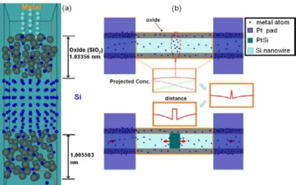
In order to understand the role of surface oxide on the Si nanowire during the diffusion process of Pt atoms. The molecular dynamics (MD) simulations were performed based on Vienna Ab-initio Simulation Package (VASP).29,30 The supercell was constructed with the existence of amorphous oxide as shown in Figure 5a.31 The thickness of the oxide layer was varied from zero to 1 nm. Without oxide, the Pt atoms dissolve rapidly into the Si and build up a high concentration profile below the Pt pads; thereby, we expect the nucleation of PtSi to occur below the contact area. With oxide, the effect of the oxide behaves like a weak diffusion barrier. The Pt atoms were found to diffuse through the oxide and distribute within the Si nanowire. The distribution length actually increases as square root of time and the concentration profile looks like a Gaussian function. In Figure 5b, the first concentration profile depicts that when we add the two concentration profiles together, the green one from the left and the purple one from right, it indicates that an up-hill diffusion of Pt has to occur. Based on the theory of nucleation and growth,32 the diffusion of both sides should stop at the middle when they meet, because beyond that the diffusion will be against the concentration gradient of the opposite side. Thus, a build-up of concentration occurs and it will lead to a flat concentration profile in the middle. The interdiffusion will lead to saturation of Pt in the Si nanowire, which will not be an equilibrium state since the system wants to form a silicide phase, and then nucleation of a silicide can occur at any place between the two contacts due to composition fluctuation; however, the most probable place will be the middle. While the build-up might lead to a small back-flow, it is negligible. When the build-up reaches the super-saturation needed, the nucleation of PtSi occurs. After that, the change, as depicted by the third concentration profile, is similar to that of a one-dimensional precipitation. The plateau in the middle is PtSi and the concentration at the Si/PtSi interface is an equilibrium concentration.
In summary, we have demonstrated that with or without surface oxide on the Si nanowire, different PtSi/Si nanowire-heterostructures appear due to different growth mechanisms by using in situ TEM observations. Specifically, when a Si nanowire has no oxide, PtSi formation starts at the contact area between the Si nanowire and the Pt pads so that a nano-heterostructure of PtSi/Si/PtSi appears. When a Si nanowire has oxide, PtSi formation starts near the center of the Si nanowire between the two Pt pads or from one end of a Si nanowire, leading to the formation of Si/PtSi/Si nanowire-heterostructures. Additionally, it has been observed that the existence of oxide seriously affects not only the growth position but also the growth behavior and rate. Molecular dynamics simulation results are coherent with our experimental observations and the proposed growth mechanisms. Since one-dimensional nano-heterostructures may have potential applications in nano-electronic devices, the
8
fundamentals of nano-heterostructure growth are of great importance for future device fabrication.
References
1. Duan, X.; Huang, Y.; Cui, Y.; Wang, J.; Lieber, C. M. Nature 2000, 409, 66-69. 2. Cui, Y.; Lieber, C. M. Science 2001, 291, 851-853.
3. Huang, Y.; Duan, X.; Cui, Y.; Lauhon, L. J.; Kim, K.; Lieber, C. M. Science 2001,
294, 1313-1317.
4. Xia, Y.; Yang, P.; Sun, Y.; Wu, Y.; Mayers, B.; Gates, B.; Yin, Y.; Kim, F.; Yan, H.
Adv. Mater. 2003, 15, 353-389.
5. Huang, Y.; Duan, X.; Cui, Y.; Lieber, C. M. Nano Lett. 2002, 2, 101-104.
6. Cui, Y.; Duan, X.; Hu, J.; Lieber, C. M. J. Phys. Chem. B 2000, 104, 5213–5216. 7. Zheng, G.; Lu, W.; Jin, S.; Lieber, C. M. Adv. Mater. 2004, 16, 1890–1893. 8. Zhong, Z.; Wang, D.; Cui, Y.; Bockrath, M. W.; Lieber, C. M. Science 2003, 302,
1377–1379.
9. Duan, X.; Niu, C.; Sahi, V.; Chen, J.; Parce, J. W.; Empedocles, S.; Goldman, J.
Nature 2003, 425, 274–278.
10. Duan, X. MRS Bull. 2007, 32, 134–141.
11. Javey, A.; Nam, S.; Friedman, R. S.; Yan, H.; Lieber, C. M. Nano Lett. 2007, 7, 773–777.
12. Patolsky, F.; Zheng, G.; Hayden, O.; Lakadamyali, M.; Zhuang, X.; Lieber, C. M.
Proc. Natl. Acad. Sci. U.S.A. 2004, 101, 14017–14022.
13. Patolsky, F.; Timko, B. P.; Zheng, G.; Lieber, C. M. MRS Bull. 2007, 32, 142–149.
14. Schmitt, A. L.; Bierman, M. J.; Schmeisser, D.; Himpsel, F. J.; Jin, S. Nano Lett.
2006, 6, 1617-1621.
15. Schmitt, A. L.; Zhu, L; Schmeisser, D.; Himpsel, F. J.; Jin, S. J. Phys. Chem.
B 2006, 110, 18142-18146.
16. Song, Y.; Schmitt, A. L.; Jin, S. Nano Lett. 2007, 7, 965-969.
17. Wu, Y.; Xiang, J.; Yang, C.; Lu, W.; Lieber, C. M. Nature 2004, 430, 61–65. 18. Lu, K. C.; Tu, K. N.; Wu, W. W.; Chen, L. J.; Yoo, B. Y.; Myung, N. V. Appl.
Phys. Lett. 2007, 90, 253111.
19. Lu, K. C.; Wu, W. W.; Wu, H. W.; Tanner, C. M.; Chang, J. P.; Chen, L. J.; Tu, K. N. Nano Lett. 2007, 7, 2389–2394.
20. Weber, W. M.; Geelhaar, L.; Graham, A. P.; Unger, E.; Duesberg, G. S.; Liebau, M.; Pamler, W.; Cheze, C.; Riechert, H.; Lugli, P.; Kreupl, F. Nano Lett. 2006, 6, 2660–2666.
9
Nano Lett. 2008, 8, 913–918.
22. Bucher, E.; Schulz, S.; Lux-Steiner, M. C.; Munz, P.; Gubler, U.; Greuter, F. Appl.
Phys. A: Mater. Sci. Process. 1986, 40, 71–77.
23. Hannon, J. B.; Kodambaka, S.; Ross, F. M.; Tromp, R. M. Nature 2006, 440, 69. 24. Cui, Y.; Lauhon, L. J.; Gudiksen, M. S.; Wang, J.; Lieber, C. M. Appl. Phys. Lett.
2001, 78, 2214-2216.
25. Wagner, R. S. ; Ellis, W. C. Appl. Phys. Lett. 1964, 4, 89-90.
26. Lin, Y. C.; Chen, Y.; Xu, D.; Huang, Y. Nano Lett. 2010, 10, 4721–4726.
27. Wu, W. W.; Lu, K. C.; Wang, C. W.; Hsieh, H. Y.; Chen, S. Y.; Chou, Y. C.; Yu, S. Y.; Chen, L. J.; Tu, K. N. Nano Lett. 2010, 10, 3984–3989.
28. Chou, Y. C.; Lu, K. C.; Tu, K. N. Mater. Sci. Eng. R-Rep. 2010, 70, 112-125. 29. Kresse, G.; Hafner, J. Phys. Rev. B 1993, 47, 558-561.
30. Kresse, G.; Furthmüller, J. Phys. Rev. B 1996, 54, 11169-11186.
31. Ouyang, H.; Chiou, H. H.; Wu, Y. C. S.; Cheng, J. H.; Ouyang, W. J. Appl. Phys.
2007, 102, 013710.
32. Porter, D. A.; Easterling, K. E. Phase Transformations in Metals and Alloys, 2nd Ed.; Nelson Thornes Publishing, 1992.
This study has been published at Nano Letters, Vol.11, No.7, 2753-2758. 本計畫相關之著作:
1. Kuo-Chang Lu*, Wen-Wei Wu*, Hao Ouyang, Yung-Chen Lin, Yu Huang, Chun-Wen Wang, Zheng-Wei Wu, Chun-Wei Huang, Lih J. Chen* and K. N. Tu, “The influence of surface oxide on the growth of metal/semiconductor
nanowires,” Nano Letters, Vol.11, No.7, 2753-2758 (2011).
(SCI) *Corresponding author
2. Shan-Chun Hsu, Cheng-Lun Hsin, Chun-Wei Huang, Shih-Ying Yu, Chun-Wen Wang, Chi-Ming Lu, Kuo-Chang Lu* and Wen-Wei Wu*, “Single-Crystalline Ge Nanowires and Cu3Ge/Ge Nano-Heterostructures,” CrystEngComm DOI: 10.1039/c2ce25316j (2012). (SCI) *Corresponding author
3. Yu-Wei Lin, Ren-You Wang, Wun-Bin Ke, I-Sheng Wang, Ying-Ta Chiu, Kuo-Chang Lu*, Kwang-Lung Lin* and Yi-Shao Lai, “The Pd distribution and Cu flow pattern of the Pd-plated Cu wire bond and their effect on the nanoindentation,” Materials Science and Engineering A, Vol. 543, 152-157 (2012). (SCI) *Corresponding author
4. Chun-Wei Huang, Cheng-Lun Hsin, Chun-Wen Wang, Fu-Hsuan Chu, Chen-Yen Kao, Jui-Yuan Chen, Yu-Ting Huang, Kuo-Chang Lu, Wen -Wei Wu and
10
Lih-Juann Chen, “Direct Observation of Melting Behaviors at Nanoscale Under Electron Beam and Heat to Form Hollow Nanostructures,” Nanoscale (accepted). (2012) (SCI)
5. Yu-Wei Lin, Ren-You Wang, Wun-Bin Ke, I-Sheng Wang, Ying-Ta Chiu, Kuo-Chang Lu*, Kwang-Lung Lin* and Yi-Shao Lai, “The influence of Pd on the interfacial reactions between the Pd-plated Cu ball bond and Al pad,”
Surface and Coatings Technology (in press). (SCI) *Corresponding author
Figures
Fig. 1 Overview of sample preparation. (a) A TEM image of a sample with
multiple sets of a Si nanowire across Pt contact pads. (b) A TEM image showing a closer look at one of the Si NW-Pt pad sets. (c) A HRTEM image of a Si nanowire with 2 nm oxide and with smooth Si/oxide interfaces. (d) A HRTEM image of a Si nanowire without oxide and with rough Si/oxide interfaces.
11
Fig. 2 Formation of single crystal PtSi nanowire and PtSi/Si/PtSi nano-heterostructures with varying length of the Si region. (a) A schematic illustration depicting growth of a PtSi/Si/PtSi nano-heterostructure. (b) A schematic illustration showing full transformation from a Si nanowire to a PtSi nanowire. (c) In situ TEM image of a Si nanowire before reaction. (d) and (e) In situ TEM images showing PtSi/Si/PtSi nano-heterostructures in which the Si regions are 575 nm and 8 nm in length, respectively. The darker region is PtSi, while the brighter region is Si. The insets in (d) are the corresponding selected area diffraction patterns of Si and PtSi, respectively. The inset in (e) is the magnification of the gap region and the scale bar is 5 nm. (f) In situ TEM image of a PtSi nanowire after reaction and full transformation from Si into PtSi.
12
Fig. 3 In situ TEM images showing different heterostructures of PtSi/Si based on
different growth mechanisms due to oxide effect. (a) In situ TEM image of a PtSi/Si/PtSi heterostructure within a Si nanowire without surface oxide. The bright area is Si and the dark area is PtSi. (b) In situ TEM image of a Si/PtSi/Si heterostructure within a Si nanowire with surface oxide. The bright area is Si and the dark area is PtSi. The inset in (b) is magnification of the heterostructure in which the scale bar is 20 nm. (c) In situ TEM image showing the formation of PtSi within an over-hang Si nanowire without oxide from a single Pt pad. The PtSi grows from the contact towards the end of the Si. (d) In situ TEM image showing the formation of PtSi within an over-hang Si nanowire with surface oxide. The PtSi grows from the end of the Si nanowire towards the Pt pad.
13
Fig.4 Schematic illustrations of oxide effect on kinetics of nano-silicide formation. (a)
A schematic illustration corresponding to Fig. 3(a), showing growth of a PtSi/Si/PtSi heterostructure within a Si nanowire without oxide. (b) A schematic illustration corresponding to Fig. 3(b), showing growth of a Si/PtSi/Si heterostructure within a Si nanowire with surface oxide. (c) A schematic illustration corresponding to Fig. 3(c), showing the PtSi formation within an over-hang Si nanowire without oxide. The growth occurs from the Pt pad to an end of the Si nanowire. (d) A schematic illustration corresponding to Fig. 3(d), showing PtSi formation within an over-hang Si nanowire with surface oxide. The growth occurs from an end of the Si nanowire to the Pt pad.
Fig. 5 Simulation of oxide effect in kinetics of nano-silicide formation. (a) Supercell
consisting of Si crystal covered with amorphous SiO2. The metal cluster situating on the top of oxide. (b) Top-view schematic plot and profiles of silicide formation with the insets of projected concentration distribution.